


Fig. 1.
Schematic layouts of (a) conventional LDMOS, (b) LDMOS-SCR and (c) SCR-LDMOS
SEMICONDUCTOR DEVICES
Hailian Liang1, 2, , Shurong Dong2, Xiaofeng Gu1, Lei Zhong2, Jian Wu2 and Zongguang Yu1, 3
Corresponding author: Gu Xiaofeng, Email:xgu@jiangnan.edu.cn
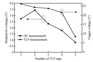
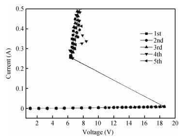
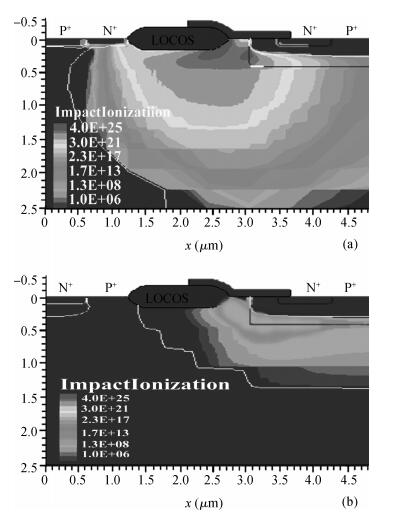
Abstract: The trigger voltage walk-in effect has been investigated by designing two different laterally diffused metal-oxide-semiconductor (LDMOS) transistors with an embedded silicon controlled rectifier (SCR). By inserting a P+ implant region along the outer and the inner boundary of the N+ region at the drain side of a conventional LDMOS transistor, we fabricate the LDMOS-SCR and the SCR-LDMOS devices with a different triggering order in a 0.5 μm bipolar-CMOS-DMOS process, respectively. First, we perform transmission line pulse (TLP) and DC-voltage degradation tests on the LDMOS-SCR. Results show that the trigger voltage walk-in effect can be attributed to the gate oxide trap generation and charge trapping. Then, we perform TLP tests on the SCR-LDMOS. Results indicate that the trigger voltage walk-in effect is remarkably reduced. In the SCR-LDMOS, the embedded SCR is triggered earlier than the LDMOS, and the ESD current is mainly discharged by the parasitic SCR structure. The electric potential between the drain and the gate decreases significantly after snapback, leading to decreased impact ionization rates and thus reduced trap generation and charge trapping. Finally, the above explanation of the different trigger voltage walk-in behavior in LDMOS-SCR and SCR-LDMOS devices is confirmed by TCAD simulation.
Key words: electrostatic discharge, laterally diffused metal-oxide-semiconductor, silicon control rectifier, trigger voltage, walk-in effect
| [1] |
Parthasarathy V, Khemka V, Zhu R, et al. A double RESURF LDMOS with drain profile engineering for improved ESD robustness. Electron Device Lett, 2002, 23(4):212 doi: 10.1109/55.992842
|
| [2] |
Qian Q S, Sun W F, Zhu J, et al. Investigation of the shift of hot spot in lateral diffused LDMOS under ESD conditions. Microelectron Reliab, 2010, 50(12):1935 doi: 10.1016/j.microrel.2010.05.010
|
| [3] |
Wang C T, Ker M D. ESD protection design with lateral DMOS transistor in 40-V BCD technology. IEEE Trans Electron Devices, 2010, 57(12):3395 doi: 10.1109/TED.2010.2079530
|
| [4] |
Griffoni A, Chen S H, Thijs S, et al. OFF-state degradation of high-voltage-tolerant nLDMOS-SCR ESD devices. IEEE Trans Electron Devices, 2011, 58(7):2061 doi: 10.1109/TED.2011.2132760
|
| [5] |
Pan H W, Liu S Y, Sun W F. A novel latch-up free SCR-LDMOS with high holding voltage for a power-rail ESD clamp. Journal of Semiconductors, 2013, 34(1):014007 doi: 10.1088/1674-4926/34/1/014007
|
| [6] |
Malobabic S, Salcedo J A, Hajjar J, et al. Analysis of safe operating area of nLDMOS and pLDMOS transistors subject to transient stresses. IEEE Trans Electron Devices, 2010, 57(10):2655 doi: 10.1109/TED.2010.2058310
|
| [7] |
Chen W Y, Ker M D. Improving safe operating area of nLDMOS array with embedded silicon controlled rectifier for ESD protection in a 24-V BCD Process. IEEE Trans Electron Devices, 2011, 58(9):2944 doi: 10.1109/TED.2011.2159861
|
| [8] |
Miao M, Dong S R, Li M L, et al. Trigger voltage walk-in effect of ESD protection device in HVCMOS. The 10th IEEE International Conference on Solid-State and Integrated Circuit Technology (ICSICT), 2010:1627
|
| [9] |
Fan H, Jiang L L, Zhang B. A novel ESD protection structure for output pads. Journal of Semiconductors, 2013, 34(11):114016 doi: 10.1088/1674-4926/34/11/114016
|
| [10] |
Mergens M P J, Wilkening W, Mettler S, et al. Analysis of lateral DMOS power devices under ESD stress conditions. IEEE Trans Electron Devices, 2000, 47(11):2128 doi: 10.1109/16.877175
|


Article views: 3894 Times PDF downloads: 66 Times Cited by: 0 Times
Received: 20 January 2014 Revised: Online: Published: 01 September 2014
| Citation: |
Hailian Liang, Shurong Dong, Xiaofeng Gu, Lei Zhong, Jian Wu, Zongguang Yu. Investigation of the trigger voltage walk-in effect in LDMOS for high-voltage ESD protection[J]. Journal of Semiconductors, 2014, 35(9): 094005. doi: 10.1088/1674-4926/35/9/094005
****
H L Liang, S R Dong, X F Gu, L Zhong, J Wu, Z G Yu. Investigation of the trigger voltage walk-in effect in LDMOS for high-voltage ESD protection[J]. J. Semicond., 2014, 35(9): 094005. doi: 10.1088/1674-4926/35/9/094005.

|
| [1] |
Parthasarathy V, Khemka V, Zhu R, et al. A double RESURF LDMOS with drain profile engineering for improved ESD robustness. Electron Device Lett, 2002, 23(4):212 doi: 10.1109/55.992842
|
| [2] |
Qian Q S, Sun W F, Zhu J, et al. Investigation of the shift of hot spot in lateral diffused LDMOS under ESD conditions. Microelectron Reliab, 2010, 50(12):1935 doi: 10.1016/j.microrel.2010.05.010
|
| [3] |
Wang C T, Ker M D. ESD protection design with lateral DMOS transistor in 40-V BCD technology. IEEE Trans Electron Devices, 2010, 57(12):3395 doi: 10.1109/TED.2010.2079530
|
| [4] |
Griffoni A, Chen S H, Thijs S, et al. OFF-state degradation of high-voltage-tolerant nLDMOS-SCR ESD devices. IEEE Trans Electron Devices, 2011, 58(7):2061 doi: 10.1109/TED.2011.2132760
|
| [5] |
Pan H W, Liu S Y, Sun W F. A novel latch-up free SCR-LDMOS with high holding voltage for a power-rail ESD clamp. Journal of Semiconductors, 2013, 34(1):014007 doi: 10.1088/1674-4926/34/1/014007
|
| [6] |
Malobabic S, Salcedo J A, Hajjar J, et al. Analysis of safe operating area of nLDMOS and pLDMOS transistors subject to transient stresses. IEEE Trans Electron Devices, 2010, 57(10):2655 doi: 10.1109/TED.2010.2058310
|
| [7] |
Chen W Y, Ker M D. Improving safe operating area of nLDMOS array with embedded silicon controlled rectifier for ESD protection in a 24-V BCD Process. IEEE Trans Electron Devices, 2011, 58(9):2944 doi: 10.1109/TED.2011.2159861
|
| [8] |
Miao M, Dong S R, Li M L, et al. Trigger voltage walk-in effect of ESD protection device in HVCMOS. The 10th IEEE International Conference on Solid-State and Integrated Circuit Technology (ICSICT), 2010:1627
|
| [9] |
Fan H, Jiang L L, Zhang B. A novel ESD protection structure for output pads. Journal of Semiconductors, 2013, 34(11):114016 doi: 10.1088/1674-4926/34/11/114016
|
| [10] |
Mergens M P J, Wilkening W, Mettler S, et al. Analysis of lateral DMOS power devices under ESD stress conditions. IEEE Trans Electron Devices, 2000, 47(11):2128 doi: 10.1109/16.877175
|

 WeChat ID
Journal of Semiconductors © 2017 All Rights Reserved 京ICP备05085259号-2

 DownLoad:

