REVIEWS

Review on the quantum emitters in two-dimensional materials

Shuliang Ren1, 2, Qinghai Tan1, 2 and Jun Zhang1, 2, 3, 4,

+ Author Affiliations

 Corresponding author: Jun Zhang, Email: zhangjwill@semi.ac.cn

PDF

Turn off MathJax

Abstract: The solid state single photon source is fundamental key device for application of quantum communication, quantum computing, quantum information and quantum precious metrology. After years of searching, researchers have found the single photon emitters in zero-dimensional quantum dots (QDs), one-dimensional nanowires, three-dimensional wide bandgap materials, as well as two-dimensional (2D) materials developed recently. Here we will give a brief review on the single photon emitters in 2D van der Waals materials. We will firstly introduce the quantum emitters from various 2D materials and their characteristics. Then we will introduce the electrically driven quantum light in the transition metal dichalcogenides (TMDs)-based light emitting diode (LED). In addition, we will introduce how to tailor the quantum emitters by nanopillars and strain engineering, the entanglement between chiral phonons (CPs) and single photon in monolayer TMDs. Finally, we will give a perspective on the opportunities and challenges of 2D materials-based quantum light sources.

Key words: two-dimensional materialssingle photon sourcequantum entanglement


[1]
Hours J, Varoutsis S, Gallart M, et al. Single photon emission from individual GaAs quantum dots. Appl Phys Lett, 2003, 82(14), 2206 doi: 10.1063/1.1563050
[2]
Stock E, Warming T, Ostapenko I, et al. Single-photon emission from InGaAs quantum dots grown on (111) GaAs. Appl Phys Lett, 2010, 96(9), 145 doi: 10.1063/1.3337097
[3]
Dalacu D, Poole P J, Williams R L. Nanowire-based sources of non-classical light. Nanotechnology, 2019, 30(23), 232001 doi: 10.1088/1361-6528/ab0393
[4]
Ma X, Hartmann N F, Baldwin J K, et al. Room-temperature single-photon generation from solitary dopants of carbon nanotubes. Nate Nanotechnol, 2015, 10(8), 671 doi: 10.1038/nnano.2015.136
[5]
Arita M, Le Roux F, Holmes M J, et al. Ultraclean single photon emission from a GaN quantum dot. Nano Lett, 2017, 17(5), 2902 doi: 10.1021/acs.nanolett.7b00109
[6]
Aharonovich I, Neu E. Diamond nanophotonics. Adv Opt Mater, 2014, 2(10), 911 doi: 10.1002/adom.v2.10
[7]
Elke N, Christian H, Michael H, et al. Low-temperature investigations of single silicon vacancy colour centres in diamond. New J Phys, 2013, 15(4), 043005 doi: 10.1088/1367-2630/15/4/043005
[8]
Aharonovich I, Zhou C, Stacey A, et al. Enhanced single-photon emission in the near infrared from a diamond color center. Phys Rev B, 2009, 79(23), 1377 doi: 10.1103/PhysRevB.79.235316
[9]
Manzeli S, Ovchinnikov D, Pasquier D, et al. 2D transition metal dichalcogenides. Nat Rev Mater, 2017, 2(8), 17033 doi: 10.1038/natrevmats.2017.33
[10]
Srivastava A, Sidler M, Allain A V, et al. Optically active quantum dots in monolayer WSe2. Nat Nanotechnol, 2015, 10(6), 491 doi: 10.1038/nnano.2015.60
[11]
Chakraborty C, Goodfellow K M, Nick V A. Localized emission from defects in MoSe2 layers. Opt Mater Express, 2016, 6(6), 2081 doi: 10.1364/OME.6.002081
[12]
Cong C, Shang J, Wang Y, Yu T. Optical properties of 2D semiconductor WS2. Adv Opt Mater, 2018, 6(1), 1700767 doi: 10.1002/adom.201700767
[13]
Hill H M, Rigosi A F, Roquelet C, et al. Observation of excitonic rydberg states in monolayer MoS2 and WS2 by photoluminescence excitation spectroscopy. Nano Lett, 2015, 15(5), 2992 doi: 10.1021/nl504868p
[14]
Koperski M, Nogajewski K, Arora A, et al. Single photon emitters in exfoliated WSe2 structures. Nat Nanotechnol, 2015, 10(6), 503 doi: 10.1038/nnano.2015.67
[15]
Chakraborty C, Kinnischtzke L, Goodfellow K M, et al. Voltage-controlled quantum light from an atomically thin semiconductor. Nat Nanotechnol, 2015, 10(6), 507 doi: 10.1038/nnano.2015.79
[16]
Ye Y, Dou X, Ding K, et al. Single photon emission from deep-level defects in monolayer WSe2. Phys Rev B, 2017, 95(24), 245313 doi: 10.1103/PhysRevB.95.245313
[17]
Qiao J D, Mei F H, Ye Y. Single-photon emitters in van der Waals materials. Chin Opt Lett, 2019, 17(2), 020011 doi: 10.3788/COL
[18]
He Y M, Clark G, Schaibley J R, et al. Single quantum emitters in monolayer semiconductors. Nat Nanotechnol, 2015, 10(6), 497 doi: 10.1038/nnano.2015.75
[19]
Tonndorf P, Schwarz S, Kern J, et al. Single-photon emitters in GaSe. 2D Mater, 2017, 4(2), 021010 doi: 10.1088/2053-1583/aa525b
[20]
Jungwirth N R, Calderon B, Ji Y, et al. Temperature dependence of wavelength selectable zero-phonon emission from single defects in hexagonal boron nitride. Nano Lett, 2016, 16(10), 6052 doi: 10.1021/acs.nanolett.6b01987
[21]
Tran T T, Zachreson C, Berhane A M, et al. Quantum emission from defects in single-crystalline hexagonal boron nitride. Phys Rev Appl, 2016, 5(3), 034005 doi: 10.1103/PhysRevApplied.5.034005
[22]
Sontheimer B, Braun M, Nikolay N, et al. Photodynamics of quantum emitters in hexagonal boron nitride revealed by low-temperature spectroscopy. Phys Rev B, 2017, 96(12), 121202 doi: 10.1103/PhysRevB.96.121202
[23]
Shotan Z, Jayakumar H, Considine C R, et al. Photoinduced modification of single-photon emitters in hexagonal boron nitride. ACS Photonics, 2016, 3(12), 2490 doi: 10.1021/acsphotonics.6b00736
[24]
Schell A W, Tran T T, Takashima H, et al. Non-linear excitation of quantum emitters in hexagonal boron nitride multiplayers. APL Photonics, 2016, 1(9), 091302 doi: 10.1063/1.4961684
[25]
Bourrellier R, Meuret S, Tararan A, et al. Bright UV single photon emission at point defects in h-BN. Nano Lett, 2016, 16(7), 4317 doi: 10.1021/acs.nanolett.6b01368
[26]
Kianinia M, Regan B, Tawfik S A, et al. Robust solid-state quantum system operating at 800 K. ACS Photonics, 2017, 4(4), 768 doi: 10.1021/acsphotonics.7b00086
[27]
Exarhos A L, Hopper D A, Patel R N, et al. Magnetic-field-dependent quantum emission in hexagonal boron nitride at room temperature. Nat Commun, 2019, 10(1), 222 doi: 10.1038/s41467-018-08185-8
[28]
Palacios-Berraquero C, Kara D M, Montblanch A R P, et al. Large-scale quantum-emitter arrays in atomically thin semiconductors. Nat Commun, 2017, 8, 15093 doi: 10.1038/NCOMMS15093
[29]
Branny A, Kumar S, Proux R, et al. Deterministic strain-induced arrays of quantum emitters in a two-dimensional semiconductor. Nat Commun, 2017, 8, 15053 doi: 10.1038/ncomms15053
[30]
Xue Y, Wang H, Tan Q, et al. Anomalous pressure characteristics of defects in hexagonal boron nitride flakes. ACS Nano, 2018, 12(7), 7127 doi: 10.1021/acsnano.8b02970
[31]
Kennard J E, Hadden J P, Marseglia L, et al. On-chip manipulation of single photons from a diamond defect. Phys Rev Lett, 2013, 111(21), 213603 doi: 10.1103/PhysRevLett.111.213603
[32]
Tran T T, Wang D, Xu Z Q, et al. Deterministic coupling of quantum emitters in 2D materials to plasmonic nanocavity arrays. Nano Lett, 2017, 17(4), 2634 doi: 10.1021/acs.nanolett.7b00444
[33]
Aharonovich I, Englund D, Toth M. Solid-state single-photon emitters. Nat Photonics, 2016, 10(10), 631 doi: 10.1038/nphoton.2016.186
[34]
Xia F, Wang H, Xiao D, et al. Two-dimensional material nanophotonics. Nat Photonics, 2014, 8(12), 899 doi: 10.1038/nphoton.2014.271
[35]
Lv R, Robinson J A, Schaak R E, et al. Transition metal dichalcogenides and beyond: synthesis, properties, and applications of single- and few-layer nanosheets. Accounts Chem Res, 2015, 48(1), 56 doi: 10.1021/ar5002846
[36]
Tran T T, Elbadawi C, Totonjian D, et al. Robust multicolor single photon emission from point defects in hexagonal boron nitride. ACS Nano, 2016, 10(8), 7331 doi: 10.1021/acsnano.6b03602
[37]
Watanabe K, Taniguchi T, Kanda H. Direct-bandgap properties and evidence for ultraviolet lasing of hexagonal boron nitride single crystal. Nat Mater, 2004, 3(6), 404 doi: 10.1038/nmat1134
[38]
Wang Q H, Kalantar-Zadeh K, Kis A, et al. Electronics and optoelectronics of two-dimensional transition metal dichalcogenides. Nat Nanotechnol, 2012, 7(11), 699 doi: 10.1038/nnano.2012.193
[39]
Yuan Z, Kardynal B E, Stevenson R M, et al. Electrically driven single-photon source. Science, 2002, 295(5552), 102 doi: 10.1126/science.1066790
[40]
Mizuochi N. Electrically driven single photon source at room temperature by using single NV center in diamond. 2013 Conference on Lasers and Electro-Optics, 2013
[41]
Schwarz S, Kozikov A, Withers F, et al. Electrically pumped single-defect light emitters in WSe2. 2D Mater, 2016, 3(2), 025038 doi: 10.1088/2053-1583/3/2/025038
[42]
Palacios-Berraquero C, Barbone M, Kara D M, et al. Atomically thin quantum light-emitting diodes. Nat Commun, 2016, 7, 12978 doi: 10.1038/ncomms12978
[43]
Hapke-Wurst I, Zeitler U, Haug R J, et al. Mapping the g factor anisotropy of InAs self-assembled quantum dots. Physica E, 2002, 12(1–4), 802 doi: 10.1016/S1386-9477(01)00428-3
[44]
Grosso G, Moon H, Lienhard B, et al. Tunable and high-purity room temperature single-photon emission from atomic defects in hexagonal boron nitride. Nat Commun, 2017, 8(1), 705 doi: 10.1038/s41467-017-00810-2
[45]
Kern J, Niehues I, Tonndorf P, et al. Nanoscale positioning of single-photon emitters in atomically Thin WSe2. Adv Mater, 2016, 28(33), 7101 doi: 10.1002/adma.201600560
[46]
Aspelmeyer M, Kippenberg T J, Marquardt F. Cavity optomechanics. Rev Mod Phys, 2014, 86(4), 1391 doi: 10.1103/RevModPhys.86.1391
[47]
Burek M J, Cohen J D, Meenehan S M, et al. Diamond optomechanical crystals. Optica, 2016, 3(12), 1404 doi: 10.1364/OPTICA.3.001404
[48]
Kepesidis K V, Bennett S D, Portolan S, et al. Phonon cooling and lasing with nitrogen-vacancy centers in diamond. Phys Rev B, 2013, 88(6), 064105 doi: 10.1103/PhysRevB.88.064105
[49]
Togan E, Chu Y, Trifonov A S, et al. Quantum entanglement between an optical photon and a solid-state spin qubit. Nature, 2010, 466(7307), 730 doi: 10.1038/nature09256
[50]
Xu X, Yao W, Xiao D, et al. Spin and pseudospins in layered transition metal dichalcogenides. Nat Phys, 2014, 10(5), 343 doi: 10.1038/nphys2942
[51]
Chen X, Lu X, Dubey S, et al. Entanglement of single-photons and chiral phonons in atomically thin WSe2. Nat Phys, 2018, 15(3), 221 doi: 10.1038/s41567-018-0366-7
[52]
Zhu H Y, Yi J, Li M Y, et al. Observation of chiral phonons. Science, 2018, 359(6375), 579 doi: 10.1126/science.aar2711
[53]
Wang L, Xu X, Zhang L, et al. Epitaxial growth of a 100-square-centimetre single-crystal hexagonal boron nitride monolayer on copper. Nature, 2019, 570(7759), 91 doi: 10.1038/s41586-019-1226-z
[54]
Tran K, Moody G, Wu F, et al. Evidence for moire excitons in van der Waals heterostructures. Nature, 2019, 567(7746), 71 doi: 10.1038/s41586-019-0975-z
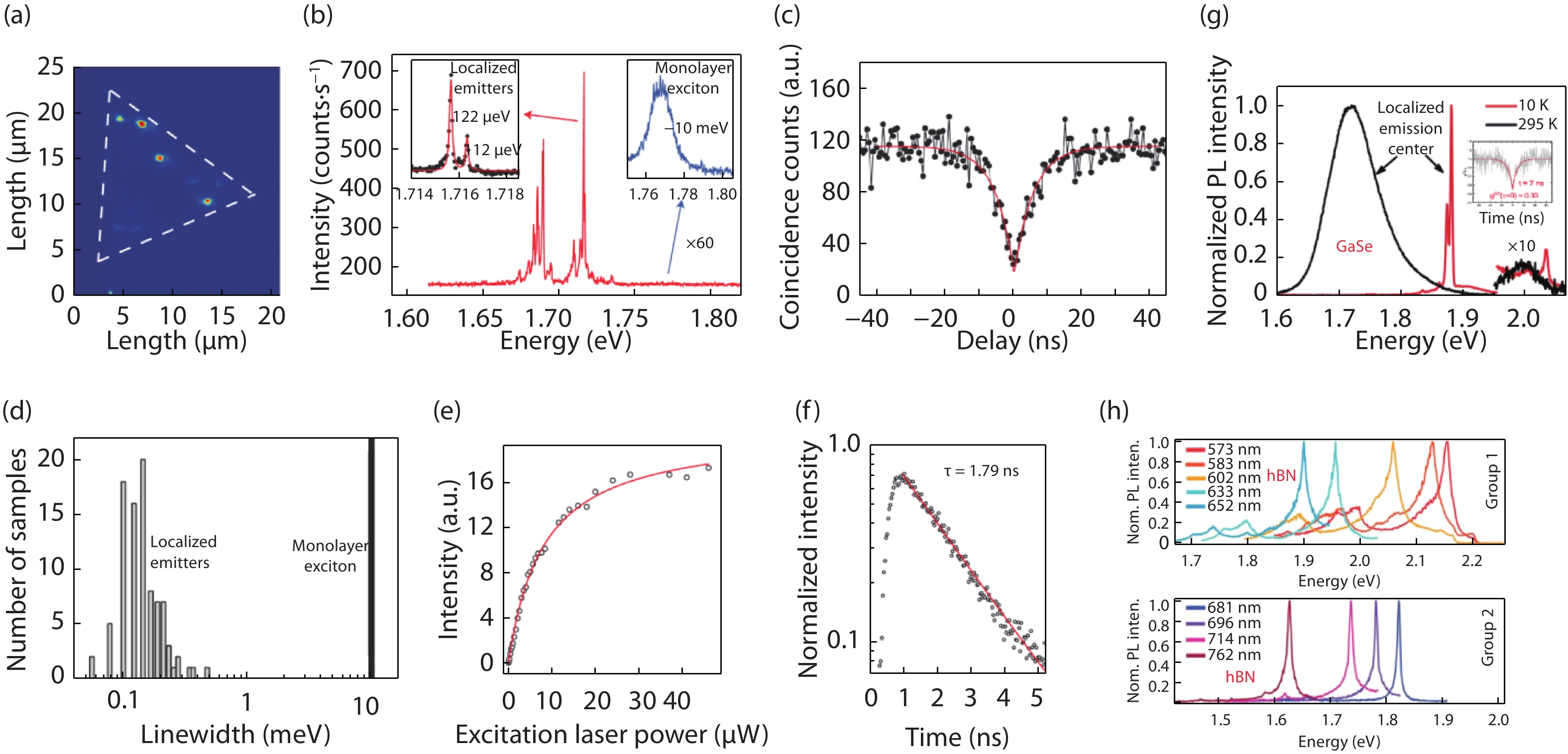
Fig. 1.  (Color online) (a) Photoluminescence (PL) intensity map of narrow emission lines centered at 1.719 eV. The dashed triangle indicates the position of the monolayer WSe2[18]. (b) PL spectrum of localized emitters. The left inset is a high resolution spectrum of one SPE. The right inset is an enlarged view of the monolayer excitons emission[18]. (c) Second order correlation measurement of the PL from one SPE in (b)[18]. (d) A histogram comparison of the linewidth between the emission from the delocalized excitons and 92 localized emitters[18]. (e) The integrated counts of the photon emission from SPE as a function of laser power. The red line is a guide to the eye[18]. (f) Time-resolved PL of SPE showing a single exponential with decay time of 1.79 ± 0.002 ns[18]. (g) Typical PL spectra of 36 nm thick GaSe, recorded at a temperature of T = 295 K and T = 10 K, respectively[19]. (h) The PL spectra of single photon emissions from hBN samples[36].

Fig. 2.  (Color online) (a) Optical microscope image of a typical device used in experiments. The dotted lines highlight the footprint of the graphene, hBN and the TMD layers individually. The Cr/Au electrodes contact the graphene and TMD layers to provide electrical bias[42]. (b) A raster-scan map of integrated EL intensity from monolayer and bilayer WSe2 areas of the quantum LED for an injection current. The dotted circles highlight the submicron localized emission in this device[42]. (c) A schematic energy band diagram, including the confined electronic states of the QDs. Electro-luminescence(EL) emission from QD starts at lower bias than the conventional LED operation threshold[42]. (d) Typical EL emission spectra for QDs in the monolayer (top) and bilayer (bottom) WSe2. The shaded area highlights the spectral window for LED emission from the bulk WSe2 excitons[42]. (e) Top (bottom) spectra of PL and EL correspond to 10 K (room temperature) operation temperature[42]. (f) Comparison of the integrated EL intensity for the WSe2 layer and for a QD as a function of the applied current. (g) Intensity-correlation function, g(2)(t) of with a rise-time of 9.4 ± 2.8 ns[42].

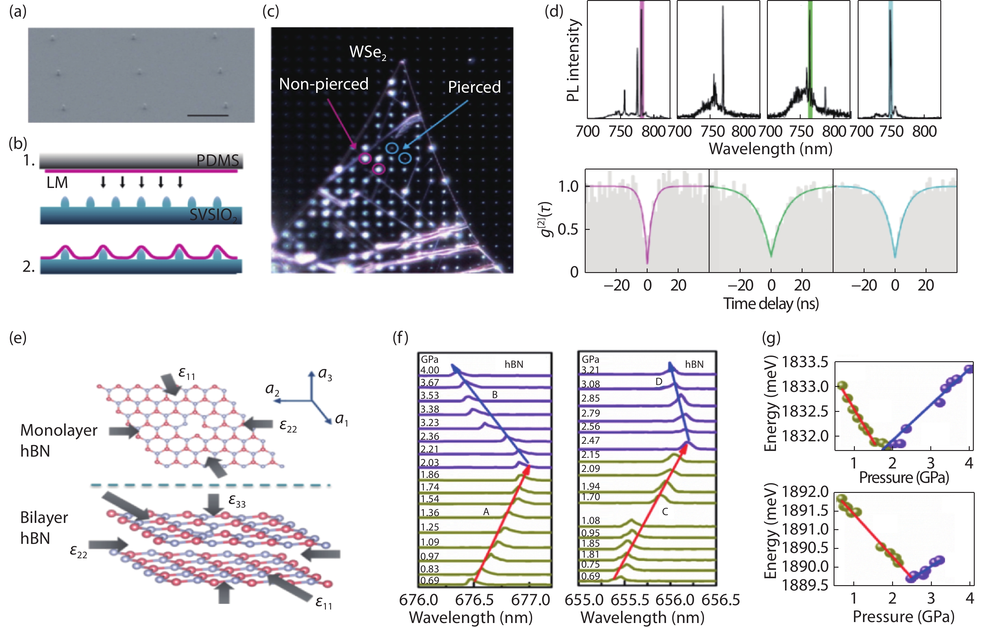
Fig. 3.  (Color online) (a) Scanning electron microscope (SEM) image of nanopillar substrate, fabricated by electron beam lithography[28]. (b) Illustration of the fabrication method: (1) mechanical exfoliation of layered materials (LM) on PDMS and all-dry viscoelastic deposition on patterned substrate; and (2) deposited LM on patterned substrate[28]. (c) Dark field optical microscopy image (real color) of monolayer layer (1L)-WSe2 on nanopillar substrate[28]. (d) PL spectra taken at nanopillar in a low orderly, enclosed by the blue, green and pink rectangles, the Second-order correlation measurement were shown below respectively[28]. (e) Schematic diagram for the strain applied in monolayer (upper part) and bilayer (lower part) geometries[30]. (f) Defect emission lines as a function of pressure, showing a redshift at a rate of 1.31(7) (peak A) and 1.33(3) meV/GPa (peak C) initially as well as a subsequent blueshift at a rate of 0.72(4) (peak B) and 0.67(9) meV/GPa (peak D), respectively, red and blue arrows are guides to the eye[30]. (g) Fitting data of the PL peak energies as a function of pressure[30].

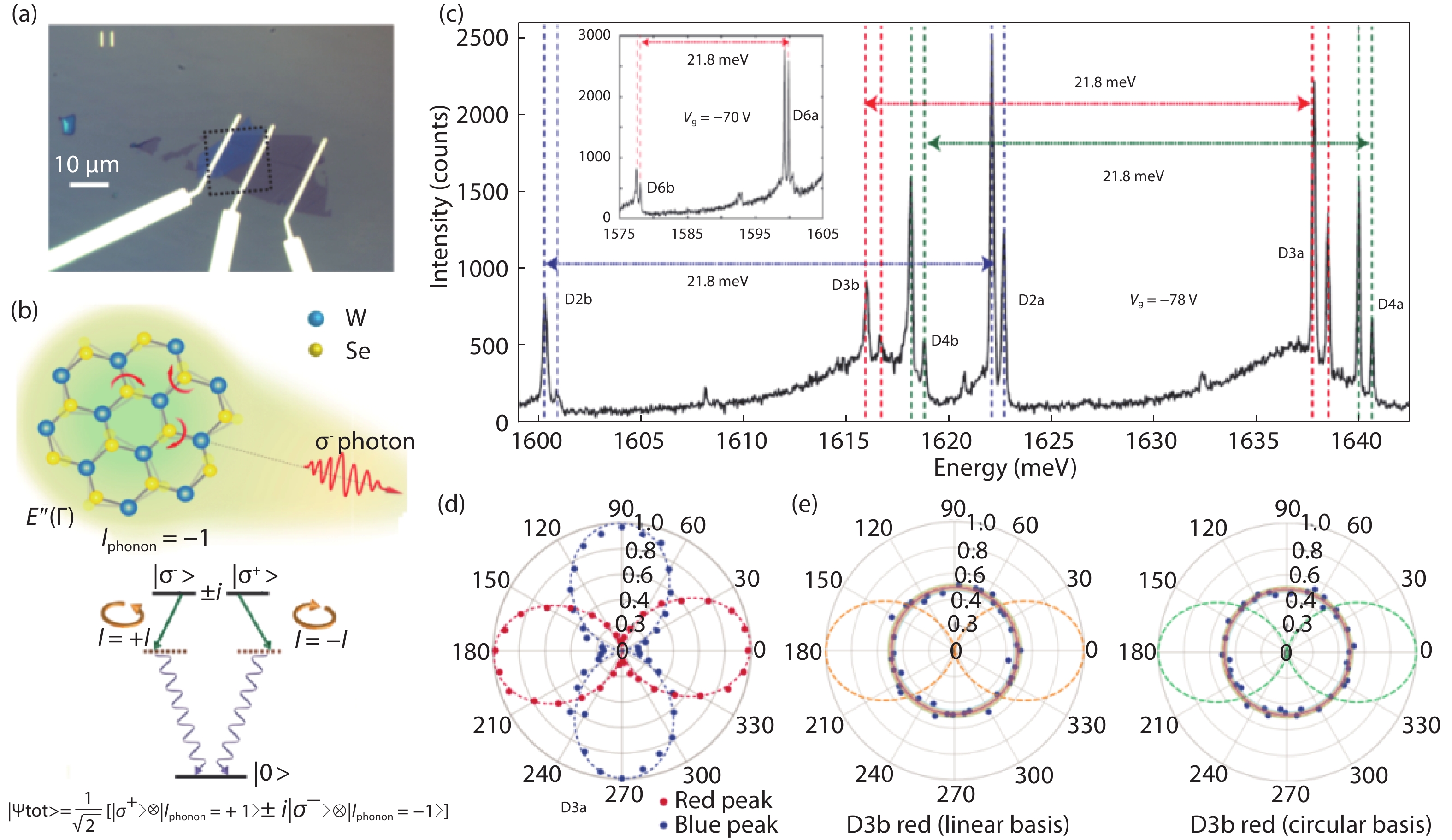
Fig. 4.  (Color online) (a) Optical image of the monolayer WSe2/hBN stack. The dashed square indicates the scanning area in the PL mapping measurements[51]. (b) Schematic of phonon–photon entanglement. The circularly polarized states (${{\rm{\sigma }}^{\rm{ - }}}{{\rm{\sigma }}^{\rm{ + }}}$) with an angular momentum of 1 = ± 1 are degenerate in WSe2 due to time-reversal symmetry[51]. (c) A PL spectrum at Vg = − 78 V. The splitting energy of the doublets is identical to that of the corresponding b doublets. The energy spacing between a and b doublets is the energy of the ${{{E}}^{''}}{}$ (Γ) phonon. Inset shows similar behavior for the QD D6[51]. (d) Polarization of the D3a doublet measured in the linear basis. The lines are ${\rm{si}}{{\rm{n}}^{\rm{2}}}{\rm{\theta /co}}{{\rm{s}}^{\rm{2}}}{\rm{\theta }}$ fits to the experimental data (dots). (e)The orange dashed line shows an example of the linearly polarized emission in the linear basis measurement, the red dashed circle with a radius of 0.5 can be either circularly polarized emission or an unpolarized light source. The green dashed line shows an example of circularly polarized emission in a circular basis measurement while the red dashed circle with a radius of 0.5 represents unpolarized emission[51].

[1]
Hours J, Varoutsis S, Gallart M, et al. Single photon emission from individual GaAs quantum dots. Appl Phys Lett, 2003, 82(14), 2206 doi: 10.1063/1.1563050
[2]
Stock E, Warming T, Ostapenko I, et al. Single-photon emission from InGaAs quantum dots grown on (111) GaAs. Appl Phys Lett, 2010, 96(9), 145 doi: 10.1063/1.3337097
[3]
Dalacu D, Poole P J, Williams R L. Nanowire-based sources of non-classical light. Nanotechnology, 2019, 30(23), 232001 doi: 10.1088/1361-6528/ab0393
[4]
Ma X, Hartmann N F, Baldwin J K, et al. Room-temperature single-photon generation from solitary dopants of carbon nanotubes. Nate Nanotechnol, 2015, 10(8), 671 doi: 10.1038/nnano.2015.136
[5]
Arita M, Le Roux F, Holmes M J, et al. Ultraclean single photon emission from a GaN quantum dot. Nano Lett, 2017, 17(5), 2902 doi: 10.1021/acs.nanolett.7b00109
[6]
Aharonovich I, Neu E. Diamond nanophotonics. Adv Opt Mater, 2014, 2(10), 911 doi: 10.1002/adom.v2.10
[7]
Elke N, Christian H, Michael H, et al. Low-temperature investigations of single silicon vacancy colour centres in diamond. New J Phys, 2013, 15(4), 043005 doi: 10.1088/1367-2630/15/4/043005
[8]
Aharonovich I, Zhou C, Stacey A, et al. Enhanced single-photon emission in the near infrared from a diamond color center. Phys Rev B, 2009, 79(23), 1377 doi: 10.1103/PhysRevB.79.235316
[9]
Manzeli S, Ovchinnikov D, Pasquier D, et al. 2D transition metal dichalcogenides. Nat Rev Mater, 2017, 2(8), 17033 doi: 10.1038/natrevmats.2017.33
[10]
Srivastava A, Sidler M, Allain A V, et al. Optically active quantum dots in monolayer WSe2. Nat Nanotechnol, 2015, 10(6), 491 doi: 10.1038/nnano.2015.60
[11]
Chakraborty C, Goodfellow K M, Nick V A. Localized emission from defects in MoSe2 layers. Opt Mater Express, 2016, 6(6), 2081 doi: 10.1364/OME.6.002081
[12]
Cong C, Shang J, Wang Y, Yu T. Optical properties of 2D semiconductor WS2. Adv Opt Mater, 2018, 6(1), 1700767 doi: 10.1002/adom.201700767
[13]
Hill H M, Rigosi A F, Roquelet C, et al. Observation of excitonic rydberg states in monolayer MoS2 and WS2 by photoluminescence excitation spectroscopy. Nano Lett, 2015, 15(5), 2992 doi: 10.1021/nl504868p
[14]
Koperski M, Nogajewski K, Arora A, et al. Single photon emitters in exfoliated WSe2 structures. Nat Nanotechnol, 2015, 10(6), 503 doi: 10.1038/nnano.2015.67
[15]
Chakraborty C, Kinnischtzke L, Goodfellow K M, et al. Voltage-controlled quantum light from an atomically thin semiconductor. Nat Nanotechnol, 2015, 10(6), 507 doi: 10.1038/nnano.2015.79
[16]
Ye Y, Dou X, Ding K, et al. Single photon emission from deep-level defects in monolayer WSe2. Phys Rev B, 2017, 95(24), 245313 doi: 10.1103/PhysRevB.95.245313
[17]
Qiao J D, Mei F H, Ye Y. Single-photon emitters in van der Waals materials. Chin Opt Lett, 2019, 17(2), 020011 doi: 10.3788/COL
[18]
He Y M, Clark G, Schaibley J R, et al. Single quantum emitters in monolayer semiconductors. Nat Nanotechnol, 2015, 10(6), 497 doi: 10.1038/nnano.2015.75
[19]
Tonndorf P, Schwarz S, Kern J, et al. Single-photon emitters in GaSe. 2D Mater, 2017, 4(2), 021010 doi: 10.1088/2053-1583/aa525b
[20]
Jungwirth N R, Calderon B, Ji Y, et al. Temperature dependence of wavelength selectable zero-phonon emission from single defects in hexagonal boron nitride. Nano Lett, 2016, 16(10), 6052 doi: 10.1021/acs.nanolett.6b01987
[21]
Tran T T, Zachreson C, Berhane A M, et al. Quantum emission from defects in single-crystalline hexagonal boron nitride. Phys Rev Appl, 2016, 5(3), 034005 doi: 10.1103/PhysRevApplied.5.034005
[22]
Sontheimer B, Braun M, Nikolay N, et al. Photodynamics of quantum emitters in hexagonal boron nitride revealed by low-temperature spectroscopy. Phys Rev B, 2017, 96(12), 121202 doi: 10.1103/PhysRevB.96.121202
[23]
Shotan Z, Jayakumar H, Considine C R, et al. Photoinduced modification of single-photon emitters in hexagonal boron nitride. ACS Photonics, 2016, 3(12), 2490 doi: 10.1021/acsphotonics.6b00736
[24]
Schell A W, Tran T T, Takashima H, et al. Non-linear excitation of quantum emitters in hexagonal boron nitride multiplayers. APL Photonics, 2016, 1(9), 091302 doi: 10.1063/1.4961684
[25]
Bourrellier R, Meuret S, Tararan A, et al. Bright UV single photon emission at point defects in h-BN. Nano Lett, 2016, 16(7), 4317 doi: 10.1021/acs.nanolett.6b01368
[26]
Kianinia M, Regan B, Tawfik S A, et al. Robust solid-state quantum system operating at 800 K. ACS Photonics, 2017, 4(4), 768 doi: 10.1021/acsphotonics.7b00086
[27]
Exarhos A L, Hopper D A, Patel R N, et al. Magnetic-field-dependent quantum emission in hexagonal boron nitride at room temperature. Nat Commun, 2019, 10(1), 222 doi: 10.1038/s41467-018-08185-8
[28]
Palacios-Berraquero C, Kara D M, Montblanch A R P, et al. Large-scale quantum-emitter arrays in atomically thin semiconductors. Nat Commun, 2017, 8, 15093 doi: 10.1038/NCOMMS15093
[29]
Branny A, Kumar S, Proux R, et al. Deterministic strain-induced arrays of quantum emitters in a two-dimensional semiconductor. Nat Commun, 2017, 8, 15053 doi: 10.1038/ncomms15053
[30]
Xue Y, Wang H, Tan Q, et al. Anomalous pressure characteristics of defects in hexagonal boron nitride flakes. ACS Nano, 2018, 12(7), 7127 doi: 10.1021/acsnano.8b02970
[31]
Kennard J E, Hadden J P, Marseglia L, et al. On-chip manipulation of single photons from a diamond defect. Phys Rev Lett, 2013, 111(21), 213603 doi: 10.1103/PhysRevLett.111.213603
[32]
Tran T T, Wang D, Xu Z Q, et al. Deterministic coupling of quantum emitters in 2D materials to plasmonic nanocavity arrays. Nano Lett, 2017, 17(4), 2634 doi: 10.1021/acs.nanolett.7b00444
[33]
Aharonovich I, Englund D, Toth M. Solid-state single-photon emitters. Nat Photonics, 2016, 10(10), 631 doi: 10.1038/nphoton.2016.186
[34]
Xia F, Wang H, Xiao D, et al. Two-dimensional material nanophotonics. Nat Photonics, 2014, 8(12), 899 doi: 10.1038/nphoton.2014.271
[35]
Lv R, Robinson J A, Schaak R E, et al. Transition metal dichalcogenides and beyond: synthesis, properties, and applications of single- and few-layer nanosheets. Accounts Chem Res, 2015, 48(1), 56 doi: 10.1021/ar5002846
[36]
Tran T T, Elbadawi C, Totonjian D, et al. Robust multicolor single photon emission from point defects in hexagonal boron nitride. ACS Nano, 2016, 10(8), 7331 doi: 10.1021/acsnano.6b03602
[37]
Watanabe K, Taniguchi T, Kanda H. Direct-bandgap properties and evidence for ultraviolet lasing of hexagonal boron nitride single crystal. Nat Mater, 2004, 3(6), 404 doi: 10.1038/nmat1134
[38]
Wang Q H, Kalantar-Zadeh K, Kis A, et al. Electronics and optoelectronics of two-dimensional transition metal dichalcogenides. Nat Nanotechnol, 2012, 7(11), 699 doi: 10.1038/nnano.2012.193
[39]
Yuan Z, Kardynal B E, Stevenson R M, et al. Electrically driven single-photon source. Science, 2002, 295(5552), 102 doi: 10.1126/science.1066790
[40]
Mizuochi N. Electrically driven single photon source at room temperature by using single NV center in diamond. 2013 Conference on Lasers and Electro-Optics, 2013
[41]
Schwarz S, Kozikov A, Withers F, et al. Electrically pumped single-defect light emitters in WSe2. 2D Mater, 2016, 3(2), 025038 doi: 10.1088/2053-1583/3/2/025038
[42]
Palacios-Berraquero C, Barbone M, Kara D M, et al. Atomically thin quantum light-emitting diodes. Nat Commun, 2016, 7, 12978 doi: 10.1038/ncomms12978
[43]
Hapke-Wurst I, Zeitler U, Haug R J, et al. Mapping the g factor anisotropy of InAs self-assembled quantum dots. Physica E, 2002, 12(1–4), 802 doi: 10.1016/S1386-9477(01)00428-3
[44]
Grosso G, Moon H, Lienhard B, et al. Tunable and high-purity room temperature single-photon emission from atomic defects in hexagonal boron nitride. Nat Commun, 2017, 8(1), 705 doi: 10.1038/s41467-017-00810-2
[45]
Kern J, Niehues I, Tonndorf P, et al. Nanoscale positioning of single-photon emitters in atomically Thin WSe2. Adv Mater, 2016, 28(33), 7101 doi: 10.1002/adma.201600560
[46]
Aspelmeyer M, Kippenberg T J, Marquardt F. Cavity optomechanics. Rev Mod Phys, 2014, 86(4), 1391 doi: 10.1103/RevModPhys.86.1391
[47]
Burek M J, Cohen J D, Meenehan S M, et al. Diamond optomechanical crystals. Optica, 2016, 3(12), 1404 doi: 10.1364/OPTICA.3.001404
[48]
Kepesidis K V, Bennett S D, Portolan S, et al. Phonon cooling and lasing with nitrogen-vacancy centers in diamond. Phys Rev B, 2013, 88(6), 064105 doi: 10.1103/PhysRevB.88.064105
[49]
Togan E, Chu Y, Trifonov A S, et al. Quantum entanglement between an optical photon and a solid-state spin qubit. Nature, 2010, 466(7307), 730 doi: 10.1038/nature09256
[50]
Xu X, Yao W, Xiao D, et al. Spin and pseudospins in layered transition metal dichalcogenides. Nat Phys, 2014, 10(5), 343 doi: 10.1038/nphys2942
[51]
Chen X, Lu X, Dubey S, et al. Entanglement of single-photons and chiral phonons in atomically thin WSe2. Nat Phys, 2018, 15(3), 221 doi: 10.1038/s41567-018-0366-7
[52]
Zhu H Y, Yi J, Li M Y, et al. Observation of chiral phonons. Science, 2018, 359(6375), 579 doi: 10.1126/science.aar2711
[53]
Wang L, Xu X, Zhang L, et al. Epitaxial growth of a 100-square-centimetre single-crystal hexagonal boron nitride monolayer on copper. Nature, 2019, 570(7759), 91 doi: 10.1038/s41586-019-1226-z
[54]
Tran K, Moody G, Wu F, et al. Evidence for moire excitons in van der Waals heterostructures. Nature, 2019, 567(7746), 71 doi: 10.1038/s41586-019-0975-z
  • Search

    Advanced Search >>

    GET CITATION

    shu

    Export: BibTex EndNote

    Article Metrics

    Article views: 5284 Times PDF downloads: 254 Times Cited by: 0 Times

    History

    Received: 30 April 2019 Revised: 12 June 2019 Online: Accepted Manuscript: 18 June 2019Uncorrected proof: 24 June 2019Published: 05 July 2019

    Catalog

      Email This Article

      User name:
      Email:*请输入正确邮箱
      Code:*验证码错误
      Shuliang Ren, Qinghai Tan, Jun Zhang. Review on the quantum emitters in two-dimensional materials[J]. Journal of Semiconductors, 2019, 40(7): 071903. doi: 10.1088/1674-4926/40/7/071903 S L Ren, Q H Tan, J Zhang, Review on the quantum emitters in two-dimensional materials[J]. J. Semicond., 2019, 40(7): 071903. doi: 10.1088/1674-4926/40/7/071903.Export: BibTex EndNote
      Citation:
      Shuliang Ren, Qinghai Tan, Jun Zhang. Review on the quantum emitters in two-dimensional materials[J]. Journal of Semiconductors, 2019, 40(7): 071903. doi: 10.1088/1674-4926/40/7/071903

      S L Ren, Q H Tan, J Zhang, Review on the quantum emitters in two-dimensional materials[J]. J. Semicond., 2019, 40(7): 071903. doi: 10.1088/1674-4926/40/7/071903.
      Export: BibTex EndNote

      Review on the quantum emitters in two-dimensional materials

      doi: 10.1088/1674-4926/40/7/071903
      More Information
      • Corresponding author: Jun Zhang, Email: zhangjwill@semi.ac.cn
      • Received Date: 2019-04-30
      • Revised Date: 2019-06-12
      • Published Date: 2019-07-01

      Catalog

        /

        DownLoad:  Full-Size Img  PowerPoint
        Return
        Return