


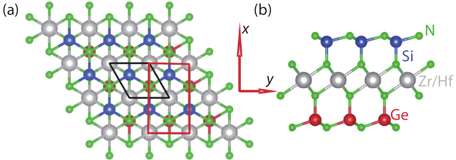
Fig. 1.
(Color online) The crystal structures of $ {\rm{MSiGe}}{{\rm{N}}_{\rm{4}}} $![]()
![]()
(M = Zr and Hf) monolayers: (a) top view and (b) side view.
ARTICLES
Xiaoshu Guo1 and Sandong Guo2,
Corresponding author: Sandong Guo, guosd@cumt.edu.cn
Abstract: A two-dimensional (2D) MA2Z4 family with
Key words: Janus monolayers, piezoelectronics, MA2Z4 family
| [1] |
Zhang L, Yang Z, Gong T, et al. Recent advances in emerging Janus two-dimensional materials: From fundamental physics to device applications. J Mater Chem A, 2020, 8, 8813 doi: 10.1039/D0TA01999B
|
| [2] |
Lu A Y, Zhu H Y, Xiao J, et al. Janus monolayers of transition metal dichalcogenides. Nat Nanotechnol, 2017, 12, 744 doi: 10.1038/nnano.2017.100
|
| [3] |
Zhang J, Jia S, Kholmanov I, et al. Janus monolayer transition-metal dichalcogenides. ACS Nano, 2017, 11, 8192 doi: 10.1021/acsnano.7b03186
|
| [4] |
Singh S, Romero A H. Giant tunable Rashba spin splitting in a two-dimensional BiSb monolayer and in BiSb/AlN heterostructures. Phys Rev B, 2017, 95, 165444 doi: 10.1103/PhysRevB.95.165444
|
| [5] |
Guo S D, Guo X S, Han R Y, et al. Predicted Janus SnSSe monolayer: A comprehensive first-principles study. Phys Chem Chem Phys, 2019, 21, 24620 doi: 10.1039/C9CP04590B
|
| [6] |
Guo Y D, Zhang H B, Zeng H L, et al. A progressive metal–semiconductor transition in two-faced Janus monolayer transition-metal chalcogenides. Phys Chem Chem Phys, 2018, 20, 21113 doi: 10.1039/C8CP02929F
|
| [7] |
Peng R, Ma Y D, Huang B B, et al. Two-dimensional Janus PtSSe for photocatalytic water splitting under the visible or infrared light. J Mater Chem A, 2019, 7, 603 doi: 10.1039/C8TA09177C
|
| [8] |
Mogulkoc A, Mogulkoc Y, Jahangirov S, et al. Characterization and stability of Janus TiXY (X/Y = S, Se, and Te) monolayers. J Phys Chem C, 2019, 123, 29922 doi: 10.1021/acs.jpcc.9b06925
|
| [9] |
Zhang C M, Nie Y H, Sanvito S, et al. First-principles prediction of a room-temperature ferromagnetic Janus VSSe monolayer with piezoelectricity, ferroelasticity, and large valley polarization. Nano Lett, 2019, 19, 1366 doi: 10.1021/acs.nanolett.8b05050
|
| [10] |
Cheng Y C, Zhu Z Y, Tahir M, et al. Spin-orbit–induced spin splittings in polar transition metal dichalcogenide monolayers. EPL, 2013, 102, 57001 doi: 10.1209/0295-5075/102/57001
|
| [11] |
Sun M L, Ren Q Q, Wang S K, et al. Electronic properties of Janus silicene: New direct band gap semiconductors. J Phys D, 2016, 49, 445305 doi: 10.1088/0022-3727/49/44/445305
|
| [12] |
Guo S D, Mu W Q, Zhu Y T, et al. Predicted septuple-atomic-layer Janus MSiGeN4 (M = Mo and W) monolayers with Rashba spin splitting and high electron carrier mobilities. J Mater Chem C, 2021, 9, 2464 doi: 10.1039/D0TC05649A
|
| [13] |
Dong L, Lou J, Shenoy V B. Large in-plane and vertical piezoelectricity in Janus transition metal dichalchogenides. ACS Nano, 2017, 11, 8242 doi: 10.1021/acsnano.7b03313
|
| [14] |
Yagmurcukardes M, Sevik C, Peeters F M. Electronic, vibrational, elastic, and piezoelectric properties of monolayer Janus MoSTe phases: A first-principles study. Phys Rev B, 2019, 100, 045415 doi: 10.1103/PhysRevB.100.045415
|
| [15] |
Zhou W H, Zhang S L, Guo S Y, et al. Designing sub-10-nm metal-oxide-semiconductor field-effect transistors via ballistic transport and disparate effective mass: The case of two-dimensional BiN. Phys Rev Appl, 2020, 13, 044066 doi: 10.1103/PhysRevApplied.13.044066
|
| [16] |
Zhou W H, Zhang S L, Wang Y Y, et al. Anisotropic in-plane ballistic transport in monolayer black arsenic- phosphorus FETs. Adv Electron Mater, 2020, 6, 1901281 doi: 10.1002/aelm.201901281
|
| [17] |
Hong Y L, Liu Z, Wang L, et al. Chemical vapor deposition of layered two-dimensional MoSi2N4 materials. Science, 2020, 369, 670 doi: 10.1126/science.abb7023
|
| [18] |
Wang L, Shi Y P, Liu M F, et al. Intercalated architecture of MA2Z4 family layered van der Waals materials with emerging topological, magnetic and superconducting properties. Nat Commun, 2021, 12, 2361 doi: 10.1038/s41467-021-22324-8
|
| [19] |
Li S, Wu W K, Feng X L, et al. Valley-dependent properties of monolayer MoSi2N4, WSi2N4, and MoSi2As4. Phys Rev B, 2020, 102, 235435 doi: 10.1103/PhysRevB.102.235435
|
| [20] |
Yang C, Song Z G, Sun X T, et al. Valley pseudospin in monolayer MoSi2N4 and MoSi2As4. Phys Rev B, 2021, 103, 035308 doi: 10.1103/PhysRevB.103.035308
|
| [21] |
Guo S D, Zhu Y T, Mu W Q, et al. Intrinsic piezoelectricity in monolayer MSi2N4 (M = Mo, W, Cr, Ti, Zr and Hf). EPL, 2020, 132, 57002 doi: 10.1209/0295-5075/132/57002
|
| [22] |
Guo S D, Zhu Y T, Mu W Q, et al. Structure effect on intrinsic piezoelectricity in septuple-atomic-layer MSi2N4 (M = Mo and W). Comput Mater Sci, 2021, 188, 110223 doi: 10.1016/j.commatsci.2020.110223
|
| [23] |
Guo S D, Mu W Q, Zhu Y T, et al. Coexistence of intrinsic piezoelectricity and ferromagnetism induced by small biaxial strain in septuple-atomic-layer VSi2P4. Phys Chem Chem Phys, 2020, 22, 28359 doi: 10.1039/D0CP05273F
|
| [24] |
Cao L M, Zhou G H, Wang Q Q, et al. Two-dimensional van der Waals electrical contact to monolayer MoSi2N4. Appl Phys Lett, 2021, 118, 013106 doi: 10.1063/5.0033241
|
| [25] |
Yu J H, Zhou J, Wan X G, et al. High intrinsic lattice thermal conductivity in monolayer MoSi2N4. New J Phys, 2021, 23, 033005 doi: 10.1088/1367-2630/abe8f7
|
| [26] |
Hohenberg P, Kohn W. Inhomogeneous electron gas. Phys Rev, 1964, 136, B864 doi: 10.1103/PhysRev.136.B864
|
| [27] |
Kresse G. Ab initio molecular dynamics for liquid metals. J Non Cryst Solids, 1995, 192/193, 222 doi: 10.1016/0022-3093(95)00355-X
|
| [28] |
Kresse G, Furthmüller J. Efficiency of ab-initio total energy calculations for metals and semiconductors using a plane-wave basis set. Comput Mater Sci, 1996, 6, 15 doi: 10.1016/0927-0256(96)00008-0
|
| [29] |
Kresse G, Joubert D. From ultrasoft pseudopotentials to the projector augmented-wave method. Phys Rev B, 1999, 59, 1758 doi: 10.1103/PhysRevB.59.1758
|
| [30] |
Perdew J P, Burke K, Ernzerhof M. Generalized gradient approximation made simple. Phys Rev Lett, 1996, 77, 3865 doi: 10.1103/PhysRevLett.77.3865
|
| [31] |
Togo A, Oba F, Tanaka I. First-principles calculations of the ferroelastic transition between rutile-type and CaCl2-type SiO2 at high pressures. Phys Rev B, 2008, 78, 134106 doi: 10.1103/PhysRevB.78.134106
|
| [32] |
Herath U, Tavadze P, He X, et al. PyProcar: A Python library for electronic structure pre/post-processing. Comput Phys Commun, 2020, 251, 107080 doi: 10.1016/j.cpc.2019.107080
|
| [33] |
Wu X F, Vanderbilt D, Hamann D R. Systematic treatment of displacements, strains, and electric fields in density-functional perturbation theory. Phys Rev B, 2005, 72, 035105 doi: 10.1103/PhysRevB.72.035105
|
| [34] |
Guo G Y, Chu K C, Wang D S, et al. Linear and nonlinear optical properties of carbon nanotubes from first-principles calculations. Phys Rev B, 2004, 69, 205416 doi: 10.1103/PhysRevB.69.205416
|
| [35] |
Andrew R C, Mapasha R E, Ukpong A M, et al. Erratum: Mechanical properties of graphene and boronitrene [Phys. Rev. B 85, 125428 (2012)]. Phys Rev B, 2004, 69, 205416 doi: 10.1103/PhysRevB.100.209901
|
| [36] |
Blonsky M N, Zhuang H L, Singh A K, et al. Ab initio prediction of piezoelectricity in two-dimensional materials. ACS Nano, 2015, 9, 9885 doi: 10.1021/acsnano.5b03394
|
| [37] |
Fei R X, Li W B, Li J, et al. Giant piezoelectricity of monolayer group IV monochalcogenides: SnSe, SnS, GeSe, and GeS. Appl Phys Lett, 2015, 107, 173104 doi: 10.1063/1.4934750
|
| [38] |
Duerloo K A N, Ong M T, Reed E J. Intrinsic piezoelectricity in two-dimensional materials. J Phys Chem Lett, 2012, 3, 2871 doi: 10.1021/jz3012436
|
| [39] |
Fan Z Q, Jiang X W, Wei Z M, et al. Tunable electronic structures of GeSe nanosheets and nanoribbons. J Phys Chem C, 2017, 121, 14373 doi: 10.1021/acs.jpcc.7b04607
|
| [40] |
Xue X X, Feng Y X, Liao L, et al. Strain tuning of electronic properties of various dimension elemental tellurium with broken screw symmetry. J Phys: Condens Matter, 2018, 30, 125001 doi: 10.1088/1361-648X/aaaea1
|
| [41] |
Guo S D, Dong J. Biaxial strain tuned electronic structures and power factor in Janus transition metal dichalchogenide monolayers. Semicond Sci Technol, 2018, 33, 085003 doi: 10.1088/1361-6641/aacb11
|
| [42] |
Gajdoš M, Hummer K, Kresse G, et al. Linear optical properties in the projector-augmented wave methodology. Phys Rev B, 2006, 73, 045112 doi: 10.1103/PhysRevB.73.045112
|
| [43] |
Huang X, Paudel T R, Dong S, et al. Hexagonal rare-earth manganites as promising photovoltaics and light polarizers. Phys Rev B, 2015, 92, 125201 doi: 10.1103/PhysRevB.92.125201
|

Table 1.
For the
| Parameter | Value |
| 3.110 (3.097) | |
| 403.92 (465.93) | |
| 110.58 (135.19) | |
| 146.67 (165.37) | |
| 373.65 (426.71) | |
| 0.274 (0.290) | |
| Gap (eV) | 1.134 (1.336) |
| Gap-SOC (eV) | 1.115 (1.282) |
 DownLoad: CSV
Table 2.
Piezoelectric Coefficients
| Zr | 2.950 | 1.006 | 0.094 | 0.018 |
| Hf | 2.251 | 0.680 | 0.068 | 0.011 |
| Mo | 5.116 | 1.494 | −0.087 | −0.014 |
| W | 3.790 | 1.050 | 0.073 | 0.011 |
DownLoad: CSV
| [1] |
Zhang L, Yang Z, Gong T, et al. Recent advances in emerging Janus two-dimensional materials: From fundamental physics to device applications. J Mater Chem A, 2020, 8, 8813 doi: 10.1039/D0TA01999B
|
| [2] |
Lu A Y, Zhu H Y, Xiao J, et al. Janus monolayers of transition metal dichalcogenides. Nat Nanotechnol, 2017, 12, 744 doi: 10.1038/nnano.2017.100
|
| [3] |
Zhang J, Jia S, Kholmanov I, et al. Janus monolayer transition-metal dichalcogenides. ACS Nano, 2017, 11, 8192 doi: 10.1021/acsnano.7b03186
|
| [4] |
Singh S, Romero A H. Giant tunable Rashba spin splitting in a two-dimensional BiSb monolayer and in BiSb/AlN heterostructures. Phys Rev B, 2017, 95, 165444 doi: 10.1103/PhysRevB.95.165444
|
| [5] |
Guo S D, Guo X S, Han R Y, et al. Predicted Janus SnSSe monolayer: A comprehensive first-principles study. Phys Chem Chem Phys, 2019, 21, 24620 doi: 10.1039/C9CP04590B
|
| [6] |
Guo Y D, Zhang H B, Zeng H L, et al. A progressive metal–semiconductor transition in two-faced Janus monolayer transition-metal chalcogenides. Phys Chem Chem Phys, 2018, 20, 21113 doi: 10.1039/C8CP02929F
|
| [7] |
Peng R, Ma Y D, Huang B B, et al. Two-dimensional Janus PtSSe for photocatalytic water splitting under the visible or infrared light. J Mater Chem A, 2019, 7, 603 doi: 10.1039/C8TA09177C
|
| [8] |
Mogulkoc A, Mogulkoc Y, Jahangirov S, et al. Characterization and stability of Janus TiXY (X/Y = S, Se, and Te) monolayers. J Phys Chem C, 2019, 123, 29922 doi: 10.1021/acs.jpcc.9b06925
|
| [9] |
Zhang C M, Nie Y H, Sanvito S, et al. First-principles prediction of a room-temperature ferromagnetic Janus VSSe monolayer with piezoelectricity, ferroelasticity, and large valley polarization. Nano Lett, 2019, 19, 1366 doi: 10.1021/acs.nanolett.8b05050
|
| [10] |
Cheng Y C, Zhu Z Y, Tahir M, et al. Spin-orbit–induced spin splittings in polar transition metal dichalcogenide monolayers. EPL, 2013, 102, 57001 doi: 10.1209/0295-5075/102/57001
|
| [11] |
Sun M L, Ren Q Q, Wang S K, et al. Electronic properties of Janus silicene: New direct band gap semiconductors. J Phys D, 2016, 49, 445305 doi: 10.1088/0022-3727/49/44/445305
|
| [12] |
Guo S D, Mu W Q, Zhu Y T, et al. Predicted septuple-atomic-layer Janus MSiGeN4 (M = Mo and W) monolayers with Rashba spin splitting and high electron carrier mobilities. J Mater Chem C, 2021, 9, 2464 doi: 10.1039/D0TC05649A
|
| [13] |
Dong L, Lou J, Shenoy V B. Large in-plane and vertical piezoelectricity in Janus transition metal dichalchogenides. ACS Nano, 2017, 11, 8242 doi: 10.1021/acsnano.7b03313
|
| [14] |
Yagmurcukardes M, Sevik C, Peeters F M. Electronic, vibrational, elastic, and piezoelectric properties of monolayer Janus MoSTe phases: A first-principles study. Phys Rev B, 2019, 100, 045415 doi: 10.1103/PhysRevB.100.045415
|
| [15] |
Zhou W H, Zhang S L, Guo S Y, et al. Designing sub-10-nm metal-oxide-semiconductor field-effect transistors via ballistic transport and disparate effective mass: The case of two-dimensional BiN. Phys Rev Appl, 2020, 13, 044066 doi: 10.1103/PhysRevApplied.13.044066
|
| [16] |
Zhou W H, Zhang S L, Wang Y Y, et al. Anisotropic in-plane ballistic transport in monolayer black arsenic- phosphorus FETs. Adv Electron Mater, 2020, 6, 1901281 doi: 10.1002/aelm.201901281
|
| [17] |
Hong Y L, Liu Z, Wang L, et al. Chemical vapor deposition of layered two-dimensional MoSi2N4 materials. Science, 2020, 369, 670 doi: 10.1126/science.abb7023
|
| [18] |
Wang L, Shi Y P, Liu M F, et al. Intercalated architecture of MA2Z4 family layered van der Waals materials with emerging topological, magnetic and superconducting properties. Nat Commun, 2021, 12, 2361 doi: 10.1038/s41467-021-22324-8
|
| [19] |
Li S, Wu W K, Feng X L, et al. Valley-dependent properties of monolayer MoSi2N4, WSi2N4, and MoSi2As4. Phys Rev B, 2020, 102, 235435 doi: 10.1103/PhysRevB.102.235435
|
| [20] |
Yang C, Song Z G, Sun X T, et al. Valley pseudospin in monolayer MoSi2N4 and MoSi2As4. Phys Rev B, 2021, 103, 035308 doi: 10.1103/PhysRevB.103.035308
|
| [21] |
Guo S D, Zhu Y T, Mu W Q, et al. Intrinsic piezoelectricity in monolayer MSi2N4 (M = Mo, W, Cr, Ti, Zr and Hf). EPL, 2020, 132, 57002 doi: 10.1209/0295-5075/132/57002
|
| [22] |
Guo S D, Zhu Y T, Mu W Q, et al. Structure effect on intrinsic piezoelectricity in septuple-atomic-layer MSi2N4 (M = Mo and W). Comput Mater Sci, 2021, 188, 110223 doi: 10.1016/j.commatsci.2020.110223
|
| [23] |
Guo S D, Mu W Q, Zhu Y T, et al. Coexistence of intrinsic piezoelectricity and ferromagnetism induced by small biaxial strain in septuple-atomic-layer VSi2P4. Phys Chem Chem Phys, 2020, 22, 28359 doi: 10.1039/D0CP05273F
|
| [24] |
Cao L M, Zhou G H, Wang Q Q, et al. Two-dimensional van der Waals electrical contact to monolayer MoSi2N4. Appl Phys Lett, 2021, 118, 013106 doi: 10.1063/5.0033241
|
| [25] |
Yu J H, Zhou J, Wan X G, et al. High intrinsic lattice thermal conductivity in monolayer MoSi2N4. New J Phys, 2021, 23, 033005 doi: 10.1088/1367-2630/abe8f7
|
| [26] |
Hohenberg P, Kohn W. Inhomogeneous electron gas. Phys Rev, 1964, 136, B864 doi: 10.1103/PhysRev.136.B864
|
| [27] |
Kresse G. Ab initio molecular dynamics for liquid metals. J Non Cryst Solids, 1995, 192/193, 222 doi: 10.1016/0022-3093(95)00355-X
|
| [28] |
Kresse G, Furthmüller J. Efficiency of ab-initio total energy calculations for metals and semiconductors using a plane-wave basis set. Comput Mater Sci, 1996, 6, 15 doi: 10.1016/0927-0256(96)00008-0
|
| [29] |
Kresse G, Joubert D. From ultrasoft pseudopotentials to the projector augmented-wave method. Phys Rev B, 1999, 59, 1758 doi: 10.1103/PhysRevB.59.1758
|
| [30] |
Perdew J P, Burke K, Ernzerhof M. Generalized gradient approximation made simple. Phys Rev Lett, 1996, 77, 3865 doi: 10.1103/PhysRevLett.77.3865
|
| [31] |
Togo A, Oba F, Tanaka I. First-principles calculations of the ferroelastic transition between rutile-type and CaCl2-type SiO2 at high pressures. Phys Rev B, 2008, 78, 134106 doi: 10.1103/PhysRevB.78.134106
|
| [32] |
Herath U, Tavadze P, He X, et al. PyProcar: A Python library for electronic structure pre/post-processing. Comput Phys Commun, 2020, 251, 107080 doi: 10.1016/j.cpc.2019.107080
|
| [33] |
Wu X F, Vanderbilt D, Hamann D R. Systematic treatment of displacements, strains, and electric fields in density-functional perturbation theory. Phys Rev B, 2005, 72, 035105 doi: 10.1103/PhysRevB.72.035105
|
| [34] |
Guo G Y, Chu K C, Wang D S, et al. Linear and nonlinear optical properties of carbon nanotubes from first-principles calculations. Phys Rev B, 2004, 69, 205416 doi: 10.1103/PhysRevB.69.205416
|
| [35] |
Andrew R C, Mapasha R E, Ukpong A M, et al. Erratum: Mechanical properties of graphene and boronitrene [Phys. Rev. B 85, 125428 (2012)]. Phys Rev B, 2004, 69, 205416 doi: 10.1103/PhysRevB.100.209901
|
| [36] |
Blonsky M N, Zhuang H L, Singh A K, et al. Ab initio prediction of piezoelectricity in two-dimensional materials. ACS Nano, 2015, 9, 9885 doi: 10.1021/acsnano.5b03394
|
| [37] |
Fei R X, Li W B, Li J, et al. Giant piezoelectricity of monolayer group IV monochalcogenides: SnSe, SnS, GeSe, and GeS. Appl Phys Lett, 2015, 107, 173104 doi: 10.1063/1.4934750
|
| [38] |
Duerloo K A N, Ong M T, Reed E J. Intrinsic piezoelectricity in two-dimensional materials. J Phys Chem Lett, 2012, 3, 2871 doi: 10.1021/jz3012436
|
| [39] |
Fan Z Q, Jiang X W, Wei Z M, et al. Tunable electronic structures of GeSe nanosheets and nanoribbons. J Phys Chem C, 2017, 121, 14373 doi: 10.1021/acs.jpcc.7b04607
|
| [40] |
Xue X X, Feng Y X, Liao L, et al. Strain tuning of electronic properties of various dimension elemental tellurium with broken screw symmetry. J Phys: Condens Matter, 2018, 30, 125001 doi: 10.1088/1361-648X/aaaea1
|
| [41] |
Guo S D, Dong J. Biaxial strain tuned electronic structures and power factor in Janus transition metal dichalchogenide monolayers. Semicond Sci Technol, 2018, 33, 085003 doi: 10.1088/1361-6641/aacb11
|
| [42] |
Gajdoš M, Hummer K, Kresse G, et al. Linear optical properties in the projector-augmented wave methodology. Phys Rev B, 2006, 73, 045112 doi: 10.1103/PhysRevB.73.045112
|
| [43] |
Huang X, Paudel T R, Dong S, et al. Hexagonal rare-earth manganites as promising photovoltaics and light polarizers. Phys Rev B, 2015, 92, 125201 doi: 10.1103/PhysRevB.92.125201
|


Article views: 1980 Times PDF downloads: 102 Times Cited by: 0 Times
Received: 10 June 2021 Revised: 21 July 2021 Online: Accepted Manuscript: 21 October 2021Uncorrected proof: 04 November 2021Published: 03 December 2021
| Citation: |
Xiaoshu Guo, Sandong Guo. Janus MSiGeN4 (M = Zr and Hf) monolayers derived from centrosymmetric β-MA2Z4: A first-principles study[J]. Journal of Semiconductors, 2021, 42(12): 122002. doi: 10.1088/1674-4926/42/12/122002
X S Guo, S D Guo, Janus MSiGeN4 (M = Zr and Hf) monolayers derived from centrosymmetric β-MA2Z4: A first-principles study[J]. J. Semicond., 2021, 42(12): 122002. doi: 10.1088/1674-4926/42/12/122002.
Export: BibTex EndNote

|
| [1] |
Zhang L, Yang Z, Gong T, et al. Recent advances in emerging Janus two-dimensional materials: From fundamental physics to device applications. J Mater Chem A, 2020, 8, 8813 doi: 10.1039/D0TA01999B
|
| [2] |
Lu A Y, Zhu H Y, Xiao J, et al. Janus monolayers of transition metal dichalcogenides. Nat Nanotechnol, 2017, 12, 744 doi: 10.1038/nnano.2017.100
|
| [3] |
Zhang J, Jia S, Kholmanov I, et al. Janus monolayer transition-metal dichalcogenides. ACS Nano, 2017, 11, 8192 doi: 10.1021/acsnano.7b03186
|
| [4] |
Singh S, Romero A H. Giant tunable Rashba spin splitting in a two-dimensional BiSb monolayer and in BiSb/AlN heterostructures. Phys Rev B, 2017, 95, 165444 doi: 10.1103/PhysRevB.95.165444
|
| [5] |
Guo S D, Guo X S, Han R Y, et al. Predicted Janus SnSSe monolayer: A comprehensive first-principles study. Phys Chem Chem Phys, 2019, 21, 24620 doi: 10.1039/C9CP04590B
|
| [6] |
Guo Y D, Zhang H B, Zeng H L, et al. A progressive metal–semiconductor transition in two-faced Janus monolayer transition-metal chalcogenides. Phys Chem Chem Phys, 2018, 20, 21113 doi: 10.1039/C8CP02929F
|
| [7] |
Peng R, Ma Y D, Huang B B, et al. Two-dimensional Janus PtSSe for photocatalytic water splitting under the visible or infrared light. J Mater Chem A, 2019, 7, 603 doi: 10.1039/C8TA09177C
|
| [8] |
Mogulkoc A, Mogulkoc Y, Jahangirov S, et al. Characterization and stability of Janus TiXY (X/Y = S, Se, and Te) monolayers. J Phys Chem C, 2019, 123, 29922 doi: 10.1021/acs.jpcc.9b06925
|
| [9] |
Zhang C M, Nie Y H, Sanvito S, et al. First-principles prediction of a room-temperature ferromagnetic Janus VSSe monolayer with piezoelectricity, ferroelasticity, and large valley polarization. Nano Lett, 2019, 19, 1366 doi: 10.1021/acs.nanolett.8b05050
|
| [10] |
Cheng Y C, Zhu Z Y, Tahir M, et al. Spin-orbit–induced spin splittings in polar transition metal dichalcogenide monolayers. EPL, 2013, 102, 57001 doi: 10.1209/0295-5075/102/57001
|
| [11] |
Sun M L, Ren Q Q, Wang S K, et al. Electronic properties of Janus silicene: New direct band gap semiconductors. J Phys D, 2016, 49, 445305 doi: 10.1088/0022-3727/49/44/445305
|
| [12] |
Guo S D, Mu W Q, Zhu Y T, et al. Predicted septuple-atomic-layer Janus MSiGeN4 (M = Mo and W) monolayers with Rashba spin splitting and high electron carrier mobilities. J Mater Chem C, 2021, 9, 2464 doi: 10.1039/D0TC05649A
|
| [13] |
Dong L, Lou J, Shenoy V B. Large in-plane and vertical piezoelectricity in Janus transition metal dichalchogenides. ACS Nano, 2017, 11, 8242 doi: 10.1021/acsnano.7b03313
|
| [14] |
Yagmurcukardes M, Sevik C, Peeters F M. Electronic, vibrational, elastic, and piezoelectric properties of monolayer Janus MoSTe phases: A first-principles study. Phys Rev B, 2019, 100, 045415 doi: 10.1103/PhysRevB.100.045415
|
| [15] |
Zhou W H, Zhang S L, Guo S Y, et al. Designing sub-10-nm metal-oxide-semiconductor field-effect transistors via ballistic transport and disparate effective mass: The case of two-dimensional BiN. Phys Rev Appl, 2020, 13, 044066 doi: 10.1103/PhysRevApplied.13.044066
|
| [16] |
Zhou W H, Zhang S L, Wang Y Y, et al. Anisotropic in-plane ballistic transport in monolayer black arsenic- phosphorus FETs. Adv Electron Mater, 2020, 6, 1901281 doi: 10.1002/aelm.201901281
|
| [17] |
Hong Y L, Liu Z, Wang L, et al. Chemical vapor deposition of layered two-dimensional MoSi2N4 materials. Science, 2020, 369, 670 doi: 10.1126/science.abb7023
|
| [18] |
Wang L, Shi Y P, Liu M F, et al. Intercalated architecture of MA2Z4 family layered van der Waals materials with emerging topological, magnetic and superconducting properties. Nat Commun, 2021, 12, 2361 doi: 10.1038/s41467-021-22324-8
|
| [19] |
Li S, Wu W K, Feng X L, et al. Valley-dependent properties of monolayer MoSi2N4, WSi2N4, and MoSi2As4. Phys Rev B, 2020, 102, 235435 doi: 10.1103/PhysRevB.102.235435
|
| [20] |
Yang C, Song Z G, Sun X T, et al. Valley pseudospin in monolayer MoSi2N4 and MoSi2As4. Phys Rev B, 2021, 103, 035308 doi: 10.1103/PhysRevB.103.035308
|
| [21] |
Guo S D, Zhu Y T, Mu W Q, et al. Intrinsic piezoelectricity in monolayer MSi2N4 (M = Mo, W, Cr, Ti, Zr and Hf). EPL, 2020, 132, 57002 doi: 10.1209/0295-5075/132/57002
|
| [22] |
Guo S D, Zhu Y T, Mu W Q, et al. Structure effect on intrinsic piezoelectricity in septuple-atomic-layer MSi2N4 (M = Mo and W). Comput Mater Sci, 2021, 188, 110223 doi: 10.1016/j.commatsci.2020.110223
|
| [23] |
Guo S D, Mu W Q, Zhu Y T, et al. Coexistence of intrinsic piezoelectricity and ferromagnetism induced by small biaxial strain in septuple-atomic-layer VSi2P4. Phys Chem Chem Phys, 2020, 22, 28359 doi: 10.1039/D0CP05273F
|
| [24] |
Cao L M, Zhou G H, Wang Q Q, et al. Two-dimensional van der Waals electrical contact to monolayer MoSi2N4. Appl Phys Lett, 2021, 118, 013106 doi: 10.1063/5.0033241
|
| [25] |
Yu J H, Zhou J, Wan X G, et al. High intrinsic lattice thermal conductivity in monolayer MoSi2N4. New J Phys, 2021, 23, 033005 doi: 10.1088/1367-2630/abe8f7
|
| [26] |
Hohenberg P, Kohn W. Inhomogeneous electron gas. Phys Rev, 1964, 136, B864 doi: 10.1103/PhysRev.136.B864
|
| [27] |
Kresse G. Ab initio molecular dynamics for liquid metals. J Non Cryst Solids, 1995, 192/193, 222 doi: 10.1016/0022-3093(95)00355-X
|
| [28] |
Kresse G, Furthmüller J. Efficiency of ab-initio total energy calculations for metals and semiconductors using a plane-wave basis set. Comput Mater Sci, 1996, 6, 15 doi: 10.1016/0927-0256(96)00008-0
|
| [29] |
Kresse G, Joubert D. From ultrasoft pseudopotentials to the projector augmented-wave method. Phys Rev B, 1999, 59, 1758 doi: 10.1103/PhysRevB.59.1758
|
| [30] |
Perdew J P, Burke K, Ernzerhof M. Generalized gradient approximation made simple. Phys Rev Lett, 1996, 77, 3865 doi: 10.1103/PhysRevLett.77.3865
|
| [31] |
Togo A, Oba F, Tanaka I. First-principles calculations of the ferroelastic transition between rutile-type and CaCl2-type SiO2 at high pressures. Phys Rev B, 2008, 78, 134106 doi: 10.1103/PhysRevB.78.134106
|
| [32] |
Herath U, Tavadze P, He X, et al. PyProcar: A Python library for electronic structure pre/post-processing. Comput Phys Commun, 2020, 251, 107080 doi: 10.1016/j.cpc.2019.107080
|
| [33] |
Wu X F, Vanderbilt D, Hamann D R. Systematic treatment of displacements, strains, and electric fields in density-functional perturbation theory. Phys Rev B, 2005, 72, 035105 doi: 10.1103/PhysRevB.72.035105
|
| [34] |
Guo G Y, Chu K C, Wang D S, et al. Linear and nonlinear optical properties of carbon nanotubes from first-principles calculations. Phys Rev B, 2004, 69, 205416 doi: 10.1103/PhysRevB.69.205416
|
| [35] |
Andrew R C, Mapasha R E, Ukpong A M, et al. Erratum: Mechanical properties of graphene and boronitrene [Phys. Rev. B 85, 125428 (2012)]. Phys Rev B, 2004, 69, 205416 doi: 10.1103/PhysRevB.100.209901
|
| [36] |
Blonsky M N, Zhuang H L, Singh A K, et al. Ab initio prediction of piezoelectricity in two-dimensional materials. ACS Nano, 2015, 9, 9885 doi: 10.1021/acsnano.5b03394
|
| [37] |
Fei R X, Li W B, Li J, et al. Giant piezoelectricity of monolayer group IV monochalcogenides: SnSe, SnS, GeSe, and GeS. Appl Phys Lett, 2015, 107, 173104 doi: 10.1063/1.4934750
|
| [38] |
Duerloo K A N, Ong M T, Reed E J. Intrinsic piezoelectricity in two-dimensional materials. J Phys Chem Lett, 2012, 3, 2871 doi: 10.1021/jz3012436
|
| [39] |
Fan Z Q, Jiang X W, Wei Z M, et al. Tunable electronic structures of GeSe nanosheets and nanoribbons. J Phys Chem C, 2017, 121, 14373 doi: 10.1021/acs.jpcc.7b04607
|
| [40] |
Xue X X, Feng Y X, Liao L, et al. Strain tuning of electronic properties of various dimension elemental tellurium with broken screw symmetry. J Phys: Condens Matter, 2018, 30, 125001 doi: 10.1088/1361-648X/aaaea1
|
| [41] |
Guo S D, Dong J. Biaxial strain tuned electronic structures and power factor in Janus transition metal dichalchogenide monolayers. Semicond Sci Technol, 2018, 33, 085003 doi: 10.1088/1361-6641/aacb11
|
| [42] |
Gajdoš M, Hummer K, Kresse G, et al. Linear optical properties in the projector-augmented wave methodology. Phys Rev B, 2006, 73, 045112 doi: 10.1103/PhysRevB.73.045112
|
| [43] |
Huang X, Paudel T R, Dong S, et al. Hexagonal rare-earth manganites as promising photovoltaics and light polarizers. Phys Rev B, 2015, 92, 125201 doi: 10.1103/PhysRevB.92.125201
|

 WeChat ID
Journal of Semiconductors © 2017 All Rights Reserved 京ICP备05085259号-2


