


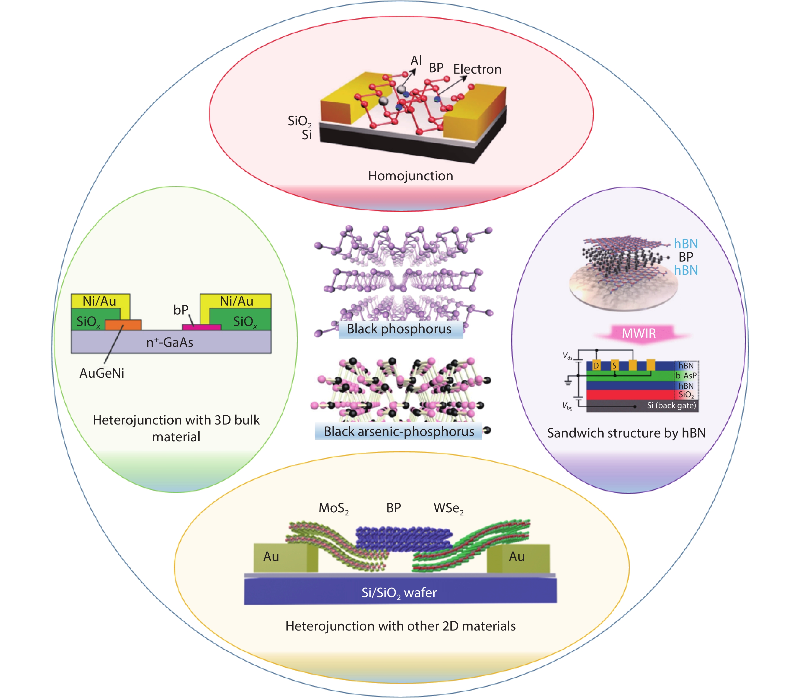
Fig. 1.
(Color online) Overview of BP crystal structure and BP devices.
REVIEWS
Ningqin Deng3, He Tian1, 2, , Jian Zhang3, Jinming Jian1, 2, Fan Wu1, 2, Yang Shen1, 2, Yi Yang1, 2 and Tian-Ling Ren1, 2,
Corresponding author: He Tian, tianhe88@tsinghua.edu.cn; Tian-Ling Ren, RenTL@tsinghua.edu.cn
Abstract: Black phosphorus (BP), an emerging two-dimensional material, is considered a promising candidate for next-generation electronic and optoelectronic devices due to in-plane anisotropy, high mobility, and direct bandgap. However, BP devices face challenges due to their limited stability, photo-response speed, and detection range. To enhance BP with powerful electrical and optical performance, the BP heterostructures can be created. In this review, the state-of-the-art heterostructures and their electrical and optoelectronic applications based on black phosphorus are discussed. Five parts introduce the performance of BP-based devices, including black phosphorus sandwich structure by hBN with better stability and higher mobility, black phosphorus homojunction by dual-gate structure for optical applications, black phosphorus heterojunction with other 2D materials for faster photo-detection, black phosphorus heterojunction integration with 3D bulk material, and BP via As-doping tunable bandgap enabling photo-detection up to 8.2 μm. Finally, we discuss the challenges and prospects for BP electrical and optical devices and applications.
Key words: black phosphorus, photodetector, heterostructure, homojunction, 2D material
| [1] |
Van Noorden R. Moving towards a graphene world. Nature, 2006, 442(7100), 228 doi: 10.1038/442228a
|
| [2] |
Sutter P. Epitaxial graphene: How silicon leaves the scene. Nat Mater, 2009, 8(3), 171 doi: 10.1038/nmat2392
|
| [3] |
Waldrop M M. The chips are down for moore's law. Nat News, 2016, 530(7589), 144 doi: 10.1038/530144a
|
| [4] |
Geim A K, Novoselov K S. The rise of graphene. Nat Mater, 2007, 6(3), 183 doi: 10.1038/nmat1849
|
| [5] |
Bolotin K I, Sikes K J, Jiang Z, et al. Ultrahigh electron mobility in suspended graphene. Solid State Commun, 2008, 146(9/10), 351 doi: 10.1016/j.ssc.2008.02.024
|
| [6] |
Balandin A A, Ghosh S, Bao W, et al. Superior thermal conductivity of single-layer graphene. Nano Lett, 2008, 8(3), 902 doi: 10.1021/nl0731872
|
| [7] |
Bae S, Kim H, Lee Y, et al. Roll-to-roll production of 30-inch graphene films for transparent electrodes. Nat Nanotechnol, 2010, 5(8), 574 doi: 10.1038/nnano.2010.132
|
| [8] |
Lee C, Wei X, Kysar J W, et al. Measurement of the elastic properties and intrinsic strength of monolayer graphene. Science, 2008, 321(5887), 385 doi: 10.1126/science.1157996
|
| [9] |
Schwierz F. Graphene transistors. Nat Nanotechnol, 2010, 5(7), 487 doi: 10.1038/nnano.2010.89
|
| [10] |
Sordan R, Traversi F, Russo V. Logic gates with a single graphene transistor. Appl Phys Lett, 2009, 94(7), 073305 doi: 10.1063/1.3079663
|
| [11] |
Deng T, Zhang Z, Liu Y, et al. Three-dimensional graphene field-effect transistors as high-performance photodetectors. Nano Lett, 2019, 19(3), 1494 doi: 10.1021/acs.nanolett.8b04099
|
| [12] |
Fang Y, Luo B, Jia Y, et al. Renewing functionalized graphene as electrodes for high-performance supercapacitors. Adv Mater, 2012, 24(47), 6348 doi: 10.1002/adma.201202774
|
| [13] |
Wang H, Yang Y, Liang Y, et al. Graphene-wrapped sulfur particles as a rechargeable lithium-sulfur battery cathode material with high capacity and cycling stability. Nano Lett, 2011, 11(7), 2644 doi: 10.1021/nl200658a
|
| [14] |
Miao X, Tongay S, Petterson M K, et al. High efficiency graphene solar cells by chemical doping. Nano Lett, 2012, 12(6), 2745 doi: 10.1021/nl204414u
|
| [15] |
Tian H, Ren T L, Xie D, et al. Graphene-on-paper sound source devices. ACS Nano, 2011, 5(6), 4878 doi: 10.1021/nn2009535
|
| [16] |
Tian H, Xie D, Yang Y, et al. Single-layer graphene sound-emitting devices: Experiments and modeling. Nanoscale, 2012, 4(7), 2272 doi: 10.1039/c2nr11572g
|
| [17] |
Zhang G, Zhang H. Thermal conduction and rectification in few-layer graphene y junctions. Nanoscale, 2011, 3(11), 4604 doi: 10.1039/c1nr10945f
|
| [18] |
Lin Y, Williams T V, Connell J W. Soluble, exfoliated hexagonal boron nitride nanosheets. J Phys Chem Lett, 2009, 1(1), 277 doi: 10.1021/jz9002108
|
| [19] |
Balendhran S, Walia S, Nili H, et al. Elemental analogues of graphene: Silicene, germanene, stanene, and phosphorene. Small, 2015, 11(6), 640 doi: 10.1002/smll.201402041
|
| [20] |
Wang Q H, Kalantar-Zadeh K, Kis A, et al. Electronics and optoelectronics of two-dimensional transition metal dichalcogenides. Nat Nanotechnol, 2012, 7(11), 699 doi: 10.1038/nnano.2012.193
|
| [21] |
Wu W, De D, Chang S C, et al. High mobility and high on/off ratio field-effect transistors based on chemical vapor deposited single-crystal MoS2 grains. Appl Phys Lett, 2013, 102(14), 142106 doi: 10.1063/1.4801861
|
| [22] |
Carvalho A, Wang M, Zhu X, et al. Phosphorene: From theory to applications. Nat Rev Mater, 2016, 1(11), 1 doi: 10.1038/natrevmats.2016.61
|
| [23] |
Bridgman P W. Two new modifications of phosphorus. J Am Chem Soc, 1914, 36(7), 1344 doi: 10.1021/ja02184a002
|
| [24] |
Liu H, Neal A T, Zhu Z, et al. Phosphorene: An unexplored 2D semiconductor with a high hole mobility. Acs Nano, 2014, 8(4), 4033 doi: 10.1021/nn501226z
|
| [25] |
Castellanos-Gomez A, Vicarelli L, Prada E, et al. Isolation and characterization of few-layer black phosphorus. 2D Mater, 2014, 1(2), 025001 doi: 10.1088/2053-1583/1/2/025001
|
| [26] |
Koenig S P, Doganov R A, Schmidt H, et al. Electric field effect in ultrathin black phosphorus. Appl Phys Lett, 2014, 104(10), 103106 doi: 10.1063/1.4868132
|
| [27] |
Tran V, Soklaski R, Liang Y, et al. Layer-controlled band gap and anisotropic excitons in few-layer black phosphorus. Phys Rev B, 2014, 89(23), 235319 doi: 10.1103/PhysRevB.89.235319
|
| [28] |
Engel M, Steiner M, Avouris P. Black phosphorus photodetector for multispectral, high-resolution imaging. Nano Lett, 2014, 14(11), 6414 doi: 10.1021/nl502928y
|
| [29] |
Li L, Yu Y, Ye G J, et al. Black phosphorus field-effect transistors. Nat Nanotechnol, 2014, 9(5), 372 doi: 10.1038/nnano.2014.35
|
| [30] |
Chen X, Wu Y, Wu Z, et al. High-quality sandwiched black phosphorus heterostructure and its quantum oscillations. Nat Commun, 2015, 6(1), 7315 doi: 10.1038/ncomms8315
|
| [31] |
Li L, Ye G J, Tran V, et al. Quantum oscillations in a two-dimensional electron gas in black phosphorus thin films. Nat Nanotechnol, 2015, 10(7), 608 doi: 10.1038/nnano.2015.91
|
| [32] |
Gillgren N, Wickramaratne D, Shi Y, et al. Gate tunable quantum oscillations in air-stable and high mobility few-layer phosphorene heterostructures. 2D Mater, 2014, 2(1), 011001 doi: 10.1088/2053-1583/2/1/011001
|
| [33] |
Fei R, Faghaninia A, Soklaski R, et al. Enhanced thermoelectric efficiency via orthogonal electrical and thermal conductances in phosphorene. Nano Lett, 2014, 14(11), 6393 doi: 10.1021/nl502865s
|
| [34] |
Lee S, Yang F, Suh J, et al. Anisotropic in-plane thermal conductivity of black phosphorus nanoribbons at temperatures higher than 100 K. Nat Commun, 2015, 6(1), 8573 doi: 10.1038/ncomms9573
|
| [35] |
Luo Z, Maassen J, Deng Y, et al. Anisotropic in-plane thermal conductivity observed in few-layer black phosphorus. Nat Commun, 2015, 6, 8572 doi: 10.1038/ncomms9572
|
| [36] |
Saito Y, Iizuka T, Koretsune T, et al. Gate-tuned thermoelectric power in black phosphorus. Nano Lett, 2016, 16(8), 4819 doi: 10.1021/acs.nanolett.6b00999
|
| [37] |
Jiang J W, Park H S. Negative poisson’s ratio in single-layer black phosphorus. Nat Commun, 2014, 5, 4727 doi: 10.1038/ncomms5727
|
| [38] |
Constantinescu G C, Hine N D M. Multipurpose black-phosphorus/hBN heterostructures. Nano Lett, 2016, 16(4), 2586 doi: 10.1021/acs.nanolett.6b00154
|
| [39] |
Cai Y, Zhang G, Zhang Y W. Electronic properties of phosphorene/graphene and phosphorene/hexagonal boron nitride heterostructures. J Phys Chem C, 2015, 119(24), 13929 doi: 10.1021/acs.jpcc.5b02634
|
| [40] |
Dean C R, Young A F, Meric I, et al. Boron nitride substrates for high-quality graphene electronics. Nat Nanotechnol, 2010, 5(10), 722 doi: 10.1038/nnano.2010.172
|
| [41] |
Chan M Y, Komatsu K, Li S L, et al. Suppression of thermally activated carrier transport in atomically thin MoS2 on crystalline hexagonal boron nitride substrates. Nanoscale, 2013, 5(20), 9572 doi: 10.1039/c3nr03220e
|
| [42] |
Lee G H, Yu Y J, Cui X, et al. Flexible and transparent MoS2 field-effect transistors on hexagonal boron nitride-graphene heterostructures. ACS Nano, 2013, 7(9), 7931 doi: 10.1021/nn402954e
|
| [43] |
Xue J, Sanchez-Yamagishi J, Bulmash D, et al. Scanning tunnelling microscopy and spectroscopy of ultra-flat graphene on hexagonal boron nitride. Nat Mater, 2011, 10(4), 282 doi: 10.1038/nmat2968
|
| [44] |
Lee C, Rathi S, Khan M A, et al. Comparison of trapped charges and hysteresis behavior in hBN encapsulated single MoS2 flake based field effect transistors on SiO2 and hBN substrates. Nanotechnology, 2018, 29(33), 335202 doi: 10.1088/1361-6528/aac6b0
|
| [45] |
Doganov R A, Koenig S P, Yeo Y, et al. Transport properties of ultrathin black phosphorus on hexagonal boron nitride. Appl Phys Lett, 2015, 106(8), 083505 doi: 10.1063/1.4913419
|
| [46] |
Cao Y, Mishchenko A, Yu G L, et al. Quality heterostructures from two-dimensional crystals unstable in air by their assembly in inert atmosphere. Nano Lett, 2015, 15(8), 4914 doi: 10.1021/acs.nanolett.5b00648
|
| [47] |
Long G, Maryenko D, Shen J, et al. Achieving ultrahigh carrier mobility in two-dimensional hole gas of black phosphorus. Nano Lett, 2016, 16(12), 7768 doi: 10.1021/acs.nanolett.6b03951
|
| [48] |
Chen X, Chen C, Levi A, et al. Large-velocity saturation in thin-film black phosphorus transistors. ACS Nano, 2018, 12(5), 5003 doi: 10.1021/acsnano.8b02295
|
| [49] |
Hu T, Hong J. Anisotropic effective mass, optical property, and enhanced band gap in hBN /phosphorene/ hBN heterostructures. ACS Appl Mater Interfaces, 2015, 7(42), 23489 doi: 10.1021/acsami.5b05694
|
| [50] |
Li L, Yang F, Ye G J, et al. Quantum hall effect in black phosphorus two-dimensional electron system. Nat Nanotechnol, 2016, 11(7), 593 doi: 10.1038/nnano.2016.42
|
| [51] |
Das S, Demarteau M, Roelofs A. Ambipolar phosphorene field effect transistor. ACS Nano, 2014, 8(11), 11730 doi: 10.1021/nn505868h
|
| [52] |
Xia F, Wang H, Jia Y. Rediscovering black phosphorus as an anisotropic layered material for optoelectronics and electronics. Nat Commun, 2014, 5(1), 4458 doi: 10.1038/ncomms5458
|
| [53] |
Du Y, Liu H, Deng Y, et al. Device perspective for black phosphorus field-effect transistors: Contact resistance, ambipolar behavior, and scaling. ACS Nano, 2014, 8(10), 10035 doi: 10.1021/nn502553m
|
| [54] |
Wang H, Wang X, Xia F, et al. Black phosphorus radio-frequency transistors. Nano Lett, 2014, 14(11), 6424 doi: 10.1021/nl5029717
|
| [55] |
Zhu W, Yogeesh M N, Yang S, et al. Flexible black phosphorus ambipolar transistors, circuits and am demodulator. Nano Lett, 2015, 15(3), 1883 doi: 10.1021/nl5047329
|
| [56] |
Kamalakar M V, Madhushankar B N, Dankert A, et al. Low schottky barrier black phosphorus field-effect devices with ferromagnetic tunnel contacts. Small, 2015, 11(18), 2209 doi: 10.1002/smll.201402900
|
| [57] |
Miao J, Zhang S, Cai L, et al. Ultrashort channel length black phosphorus field-effect transistors. ACS Nano, 2015, 9(9), 9236 doi: 10.1021/acsnano.5b04036
|
| [58] |
Prakash A, Cai Y, Zhang G, et al. Black phosphorus n-type field-effect transistor with ultrahigh electron mobility via aluminum adatoms doping. Small, 2017, 13(5), 1602909 doi: 10.1002/smll.201602909
|
| [59] |
Han C, Hu Z, Gomes L C, et al. Surface functionalization of black phosphorus via potassium toward high-performance complementary devices. Nano Lett, 2017, 17(7), 4122 doi: 10.1021/acs.nanolett.7b00903
|
| [60] |
Liu Y, Cai Y, Zhang G, et al. Al-doped black phosphorus p–n homojunction diode for high performance photovoltaic. Adv Funct Mater, 2017, 27(7), 1604638 doi: 10.1002/adfm.201604638
|
| [61] |
Avsar A, Vera-Marun I J, Tan J Y, et al. Air-stable transport in graphene-contacted, fully encapsulated ultrathin black phosphorus-based field-effect transistors. ACS Nano, 2015, 9(4), 4138 doi: 10.1021/acsnano.5b00289
|
| [62] |
Xu J, Jia J, Lai S, et al. Tunneling field effect transistor integrated with black phosphorus-MoS2 junction and ion gel dielectric. Appl Phys Lett, 2017, 110(3), 033103 doi: 10.1063/1.4974303
|
| [63] |
Liu X, Qu D, Li H M, et al. Modulation of quantum tunneling via a vertical two-dimensional black phosphorus and molybdenum disulfide p–n junction. ACS Nano, 2017, 11(9), 9143 doi: 10.1021/acsnano.7b03994
|
| [64] |
Kang J, Jariwala D, Ryder C R, et al. Probing out-of-plane charge transport in black phosphorus with graphene-contacted vertical field-effect transistors. Nano Lett, 2016, 16(4), 2580 doi: 10.1021/acs.nanolett.6b00144
|
| [65] |
Buscema M, Groenendijk D J, Steele G A, et al. Photovoltaic effect in few-layer black phosphorus pn junctions defined by local electrostatic gating. Nat Commun, 2014, 5(1), 4651 doi: 10.1038/ncomms5651
|
| [66] |
Tian H, Li L, Mohammad M A, et al. High-quality reconfigurable black phosphorus p–n junctions. IEEE Trans Electron Devices, 2018, 65(11), 5118 doi: 10.1109/TED.2018.2869268
|
| [67] |
Buscema M, Groenendijk D J, Blanter S I, et al. Fast and broadband photoresponse of few-layer black phosphorus field-effect transistors. Nano Lett, 2014, 14(6), 3347 doi: 10.1021/nl5008085
|
| [68] |
Wu J, Koon G K, Xiang D, et al. Colossal ultraviolet photoresponsivity of few-layer black phosphorus. ACS Nano, 2015, 9(8), 8070 doi: 10.1021/acsnano.5b01922
|
| [69] |
Huang M, Wang M, Chen C, et al. Broadband black-phosphorus photodetectors with high responsivity. Adv Mater, 2016, 28(18), 3481 doi: 10.1002/adma.201506352
|
| [70] |
Guo Q, Pospischil A, Bhuiyan M, et al. Black phosphorus mid-infrared photodetectors with high gain. Nano Lett, 2016, 16(7), 4648 doi: 10.1021/acs.nanolett.6b01977
|
| [71] |
Hou C, Yang L, Li B, et al. Multilayer black phosphorus near-infrared photodetectors. Sensors, 2018, 18(6), 1668 doi: 10.3390/s18061668
|
| [72] |
Deng Y, Luo Z, Conrad N J, et al. Black phosphorus-monolayer MoS2 van der Waals heterojunction p–n diode. ACS Nano, 2014, 8(8), 8292 doi: 10.1021/nn5027388
|
| [73] |
Hong T, Chamlagain B, Wang T, et al. Anisotropic photocurrent response at black phosphorus–MoS2 p–n heterojunctions. Nanoscale, 2015, 7(44), 18537 doi: 10.1039/C5NR03400K
|
| [74] |
Ye L, Li H, Chen Z, et al. Near-infrared photodetector based on MoS2/black phosphorus heterojunction. ACS Photonics, 2016, 3(4), 692 doi: 10.1021/acsphotonics.6b00079
|
| [75] |
Li H, Ye L, Xu J. High-performance broadband floating-base bipolar phototransistor based on WSe2/bp/MoS2 heterostructure. ACS Photonics, 2017, 4(4), 823 doi: 10.1021/acsphotonics.6b00778
|
| [76] |
Srivastava P K, Hassan Y, Gebredingle Y, et al. Van der waals broken-gap p–n heterojunction tunnel diode based on black phosphorus and rhenium disulfide. ACS Appl Mater Interfaces, 2019, 11(8), 8266 doi: 10.1021/acsami.8b22103
|
| [77] |
Huang L, Huo N, Li Y, et al. Electric-field tunable band offsets in black phosphorus and MoS2 van der Waals p–n heterostructure. J Phys Chem Lett, 2015, 6(13), 2483 doi: 10.1021/acs.jpclett.5b00976
|
| [78] |
Wang X, Lan S. Optical properties of black phosphorus. Adv Opt Photonics, 2016, 8(4), 618 doi: 10.1364/AOP.8.000618
|
| [79] |
Liu H, Du Y, Deng Y, et al. Semiconducting black phosphorus: Synthesis, transport properties and electronic applications. Chem Soc Rev, 2015, 44(9), 2732 doi: 10.1039/C4CS00257A
|
| [80] |
Chen H, Liu H, Zhang Z, et al. Nanostructured photodetectors: From ultraviolet to terahertz. Adv Mater, 2016, 28(3), 403 doi: 10.1002/adma.201503534
|
| [81] |
Youngblood N, Chen C, Koester S J, et al. Waveguide-integrated black phosphorus photodetector with high responsivity and low dark current. Nat Photonics, 2015, 9(4), 247 doi: 10.1038/nphoton.2015.23
|
| [82] |
Hu W, Wang T, Yang J. Tunable schottky contacts in hybrid graphene–phosphorene nanocomposites. J Mater Chem C, 2015, 3(18), 4756 doi: 10.1039/C5TC00759C
|
| [83] |
Song J, Yu Z, Gordin M L, et al. Chemically bonded phosphorus/graphene hybrid as a high performance anode for sodium-ion batteries. Nano Lett, 2014, 14(11), 6329 doi: 10.1021/nl502759z
|
| [84] |
Yu Z, Song J, Gordin M L, et al. Phosphorus-graphene nanosheet hybrids as lithium-ion anode with exceptional high-temperature cycling stability. Adv Sci, 2015, 2(1/2), 1400020 doi: 10.1002/advs.201400020
|
| [85] |
Li M, Muralidharan N, Moyer K, et al. Solvent mediated hybrid 2D materials: Black phosphorus – graphene heterostructured building blocks assembled for sodium ion batteries. Nanoscale, 2018, 10(22), 10443 doi: 10.1039/C8NR01400K
|
| [86] |
Liu Y, Liu Q, Zhang A, et al. Room-temperature pressure synthesis of layered black phosphorus-graphene composite for sodium-ion battery anodes. ACS Nano, 2018, 12(8), 8323 doi: 10.1021/acsnano.8b03615
|
| [87] |
Manzeli S, Ovchinnikov D, Pasquier D, et al. 2D transition metal dichalcogenides. Nat Rev Mater, 2017, 2(8), 17033 doi: 10.1038/natrevmats.2017.33
|
| [88] |
Lopez-Sanchez O, Lembke D, Kayci M, et al. Ultrasensitive photodetectors based on monolayer MoS2. Nat Nanotechnol, 2013, 8(7), 497 doi: 10.1038/nnano.2013.100
|
| [89] |
Yin Z, Li H, Li H, et al. Single-layer MoS2 phototransistors. ACS Nano, 2012, 6(1), 74 doi: 10.1021/nn2024557
|
| [90] |
Lee H S, Min S W, Chang Y G, et al. MoS2 nanosheet phototransistors with thickness-modulated optical energy gap. Nano Lett, 2012, 12(7), 3695 doi: 10.1021/nl301485q
|
| [91] |
Kwak D H, Ra H S, Jeong M H, et al. High-performance photovoltaic effect with electrically balanced charge carriers in black phosphorus and WS2 heterojunction. Adv Mater Interfaces, 2018, 5(18), 1800671 doi: 10.1002/admi.201800671
|
| [92] |
Miao J, Xu Z, Li Q, et al. Vertically stacked and self-encapsulated van der Waals heterojunction diodes using two-dimensional layered semiconductors. ACS Nano, 2017, 11(10), 10472 doi: 10.1021/acsnano.7b05755
|
| [93] |
Jariwala D, Marks T J, Hersam M C. Mixed-dimensional van der Waals heterostructures. Nat Mater, 2017, 16(2), 170 doi: 10.1038/nmat4703
|
| [94] |
Gehring P, Urcuyo R, Duong D L, et al. Thin-layer black phosphorus/gaas heterojunction p –n diodes. Appl Phys Lett, 2015, 106(23), 233110 doi: 10.1063/1.4922531
|
| [95] |
Liu B, Kopf M, Abbas A N, et al. Black arsenic-phosphorus: Layered anisotropic infrared semiconductors with highly tunable compositions and properties. Adv Mater, 2015, 27(30), 4423 doi: 10.1002/adma.201501758
|
| [96] |
Li C, Chen C, Chen J, et al. High-performance junction field-effect transistor based on black phosphorus/β-Ga2O3 heterostructure. J Semicond, 2020, 41(8), 082002 doi: 10.1088/1674-4926/41/8/082002
|
| [97] |
Long M, Gao A, Wang P, et al. Room temperature high-detectivity mid-infrared photodetectors based on black arsenic phosphorus. Sci Adv, 2017, 3(6), e1700589 doi: 10.1126/sciadv.1700589
|
| [98] |
Yuan S, Shen C, Deng B, et al. Air-stable room-temperature mid-infrared photodetectors based on hBN/black arsenic phosphorus/ hBN heterostructures. Nano Lett, 2018, 18(5), 3172 doi: 10.1021/acs.nanolett.8b00835
|
| [99] |
Koenig S P, Doganov R A, Seixas L, et al. Electron doping of ultrathin black phosphorus with Cu adatoms. Nano Lett, 2016, 16(4), 2145 doi: 10.1021/acs.nanolett.5b03278
|
| [100] |
Chen L, Li S, Feng X W, et al. Gigahertz integrated circuits based on complementary black phosphorus transistors. Adv Electron Mater, 2018, 4(9), 1800274 doi: 10.1002/aelm.201800274
|
| [101] |
Gao G, Wan B, Liu X, et al. Tunable tribotronic dual-gate logic devices based on 2D MoS2 and black phosphorus. Adv Mater, 2018, 30(13), 1705088 doi: 10.1002/adma.201705088
|
| [102] |
Perello D J, Chae S H, Song S, et al. High-performance n-type black phosphorus transistors with type control via thickness and contact-metal engineering. Nat Commun, 2015, 6(1), 7809 doi: 10.1038/ncomms8809
|
| [103] |
Favron A, Gaufrès E, Fossard F, et al. Photooxidation and quantum confinement effects in exfoliated black phosphorus. Nat Mater, 2015, 14(8), 826 doi: 10.1038/nmat4299
|
| [104] |
Tian H, Guo Q, Xie Y, et al. Anisotropic black phosphorus synaptic device for neuromorphic applications. Adv Mater, 2016, 28(25), 4991 doi: 10.1002/adma.201600166
|
| [105] |
Wood J D, Wells S A, Jariwala D, et al. Effective passivation of exfoliated black phosphorus transistors against ambient degradation. Nano Lett, 2014, 14(12), 6964 doi: 10.1021/nl5032293
|
| [106] |
Ryder C R, Wood J D, Wells S A, et al. Covalent functionalization and passivation of exfoliated black phosphorus via aryl diazonium chemistry. Nat Chem, 2016, 8(6), 597 doi: 10.1038/nchem.2505
|
| [107] |
Xu Y, Shi X, Zhang Y, et al. Epitaxial nucleation and lateral growth of high-crystalline black phosphorus films on silicon. Nat Commun, 2020, 11(1), 1330 doi: 10.1038/s41467-020-14902-z
|
| [108] |
Wachter S, Polyushkin D K, Bethge O, et al. A microprocessor based on a two-dimensional semiconductor. Nat Commun, 2017, 8(1), 14948 doi: 10.1038/ncomms14948
|
| [109] |
Bi J, Zou X, Lv Y, et al. Ingazno tunnel and junction transistors based on vertically stacked black phosphorus/ingazno heterojunctions. Adv Electron Mater, 2020, 6(8), 2000291 doi: 10.1002/aelm.202000291
|
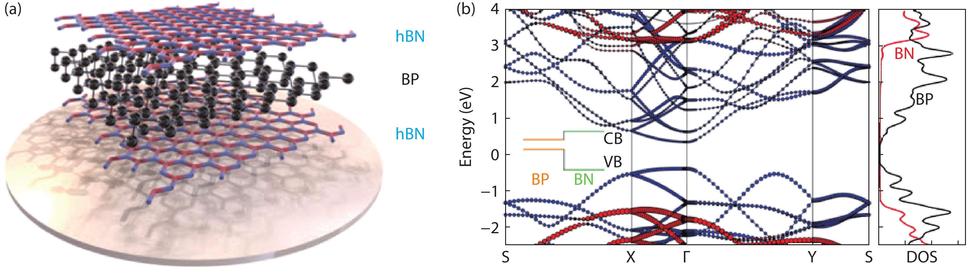
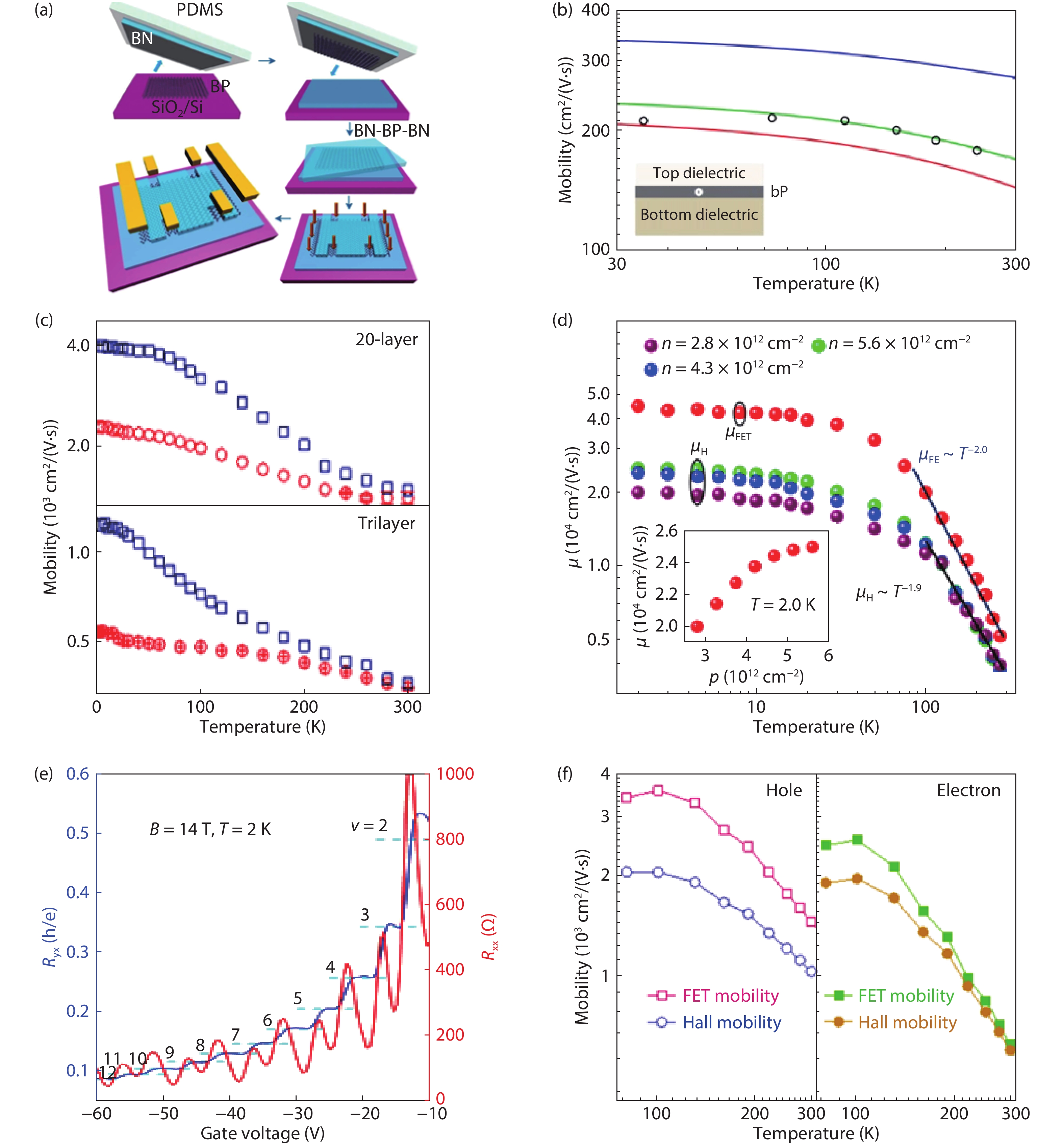
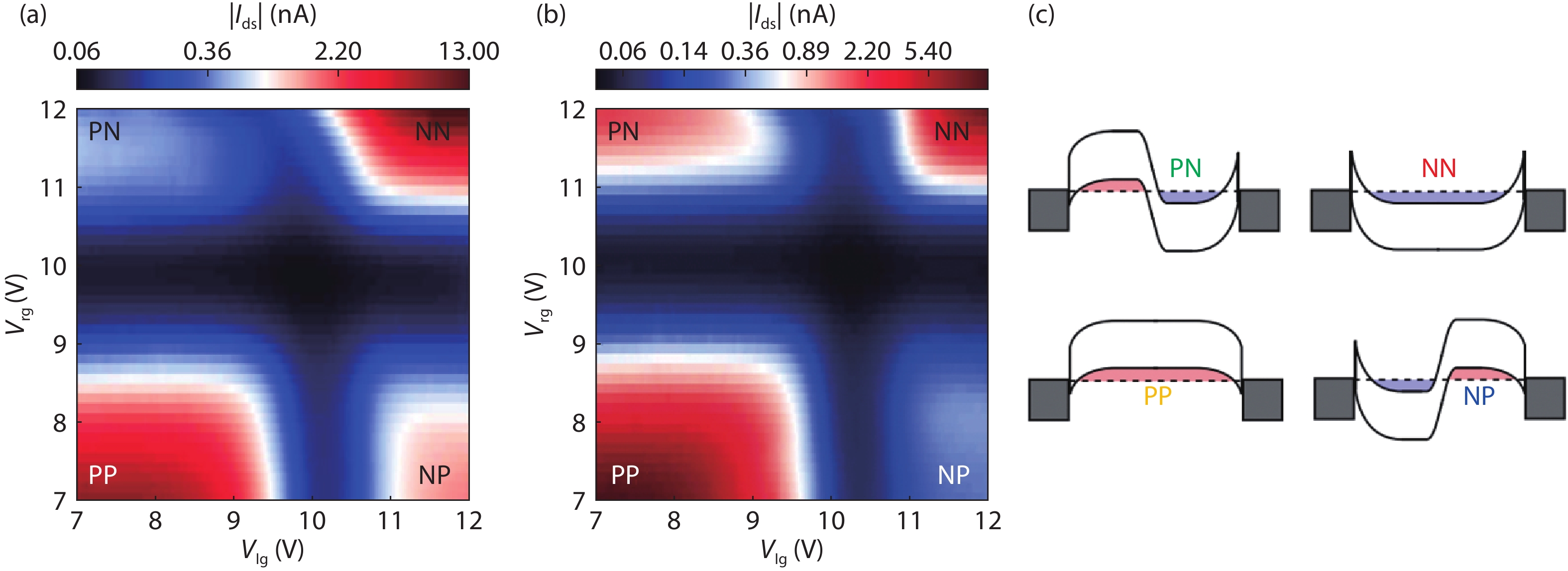
Table 1. Comparison of performance of FETs based on BP and BP heterostructures, including BP film thickness, structure, mobility, on/off ratio.
| Film thickness (nm) | Structure | Mobility (cm2/(V·s)) | On/off ratio | Experimental temperature (K) | Ref. |
| 10 | BP | 286 | 104 | Room temperature | [24] |
| 10 | BP | 984 | 105 | Room temperature | [29] |
| 1.9 | BP | 172 | 2.7×10⁴ | Room temperature | [51] |
| 5 | BP | 205 | 105 | Room temperature | [52] |
| 15 | BP | 1000 | 104 | 120 K | |
| 18.7 | BP | 170.5 | 102 | Room temperature | [53] |
| 8.5 | BP | 400 | 2×10³ | Room temperature | [54] |
| 15 | BP | 310 | 103~104 | Room temperature | [55] |
| 5 | BP | 180 | 104~105 | Room temperature | |
| 5 | BP | 155 | 104 | Room temperature | [56] |
| 8 | hBN/BP/hBN | 1350 | 105 | Room temperature | [30] |
| 2700 | / | 1.7 K | |||
| / | hBN/BP/hBN | 5200 | / | Room temperature | [47] |
| / | 45000 | / | 2 K | ||
| 11 | hBN/BP/hBN | 1432 | 103 | Room temperature | [48] |
| 3388 | / | 77 K | |||
| 10 | BP | 17 | 102 | Room temperature | [57] |
| 5 | BP | 1495 | 103 | 260 K | [58] |
| 6.5 | BP(K-doped) | 262 | 104 | Room temperature | [59] |
| 2.5 | BP(Al-doped) | 105 | 5.6×10³ | Room temperature | [60] |
| 4.5 | hBN/graphene/BP | 63 | 100 | Room temperature | [61] |
| 30 | BP/MoS2 | / | 104 | Room temperature | [62] |
| 72 | BP/MoS2 | / | 105 | Room temperature | [63] |
| 10–15 | Graphene/BP | / | 800 | 30 K | [64] |
 DownLoad: CSV
Table 2. Comparison of performance of photodetectors based on BP and BP-related heterostructures, including film thickness, structure, spectral range, responsivity, specific detectivity and response time.
| Film thickness (nm) | Structure | Spectral range | Responsivity (A/W) | Specific detectivity (Jones) | Response time (ms) | Ref. |
| BP: 3–8 | BP | Visible to near-infrared | 4.8 × 10⁻³ (640 nm) | >103 | ~1 | [67] |
| BP: ~4.5 | BP | Near-ultraviolet to near-infrared | 9 × 10⁴ (405 nm) | 3 × 10¹³ | ~1 | [68] |
| BP: 8 | BP | Visible to near-infrared | 4.3 × 10⁶ (633 nm, 300 K) 7 × 10⁶ (633 nm, 20 K) | / | 5 | [69] |
| BP: ~12 | BP | 532 nm | 82 | / | / | [70] |
| BP: 28, 47, 302 | BP | 830 nm | 2.42 | 1.833 × 10⁸ | 2.5 | [71] |
| BP: ~22 | BP/MoS2 | 633 nm | 0.418 | / | / | [72] |
| BP: ~10, MoS2: ~4.8 | BP/MoS2 | 532 nm | ~0.17 | / | / | [73] |
| BP: ~22, MoS2: ~12 | BP/MoS2 | Visible to near-infrared | 22.3 (532 nm) 153.4 (1.55 μm) | 3.1 × 10¹¹ (532 nm) 2.13 × 10⁹ (1.55 μm) | 0.015 / | [74] |
| BP: 5, ReS2: 12 | BP/ReS2 | 532 nm | 8 | / | / | [75] |
| WSe2: ~43, BP: ~40, MoS2: ~34 | WSe2/BP/MoS2 | Visible to near-infrared | 6.32 (532 nm) 1.12 (1.55 μm) | 1.25 × 10¹¹ (532 nm) 2.21 × 10¹⁰ (1.55 μm) | / | [76] |
DownLoad: CSV
| [1] |
Van Noorden R. Moving towards a graphene world. Nature, 2006, 442(7100), 228 doi: 10.1038/442228a
|
| [2] |
Sutter P. Epitaxial graphene: How silicon leaves the scene. Nat Mater, 2009, 8(3), 171 doi: 10.1038/nmat2392
|
| [3] |
Waldrop M M. The chips are down for moore's law. Nat News, 2016, 530(7589), 144 doi: 10.1038/530144a
|
| [4] |
Geim A K, Novoselov K S. The rise of graphene. Nat Mater, 2007, 6(3), 183 doi: 10.1038/nmat1849
|
| [5] |
Bolotin K I, Sikes K J, Jiang Z, et al. Ultrahigh electron mobility in suspended graphene. Solid State Commun, 2008, 146(9/10), 351 doi: 10.1016/j.ssc.2008.02.024
|
| [6] |
Balandin A A, Ghosh S, Bao W, et al. Superior thermal conductivity of single-layer graphene. Nano Lett, 2008, 8(3), 902 doi: 10.1021/nl0731872
|
| [7] |
Bae S, Kim H, Lee Y, et al. Roll-to-roll production of 30-inch graphene films for transparent electrodes. Nat Nanotechnol, 2010, 5(8), 574 doi: 10.1038/nnano.2010.132
|
| [8] |
Lee C, Wei X, Kysar J W, et al. Measurement of the elastic properties and intrinsic strength of monolayer graphene. Science, 2008, 321(5887), 385 doi: 10.1126/science.1157996
|
| [9] |
Schwierz F. Graphene transistors. Nat Nanotechnol, 2010, 5(7), 487 doi: 10.1038/nnano.2010.89
|
| [10] |
Sordan R, Traversi F, Russo V. Logic gates with a single graphene transistor. Appl Phys Lett, 2009, 94(7), 073305 doi: 10.1063/1.3079663
|
| [11] |
Deng T, Zhang Z, Liu Y, et al. Three-dimensional graphene field-effect transistors as high-performance photodetectors. Nano Lett, 2019, 19(3), 1494 doi: 10.1021/acs.nanolett.8b04099
|
| [12] |
Fang Y, Luo B, Jia Y, et al. Renewing functionalized graphene as electrodes for high-performance supercapacitors. Adv Mater, 2012, 24(47), 6348 doi: 10.1002/adma.201202774
|
| [13] |
Wang H, Yang Y, Liang Y, et al. Graphene-wrapped sulfur particles as a rechargeable lithium-sulfur battery cathode material with high capacity and cycling stability. Nano Lett, 2011, 11(7), 2644 doi: 10.1021/nl200658a
|
| [14] |
Miao X, Tongay S, Petterson M K, et al. High efficiency graphene solar cells by chemical doping. Nano Lett, 2012, 12(6), 2745 doi: 10.1021/nl204414u
|
| [15] |
Tian H, Ren T L, Xie D, et al. Graphene-on-paper sound source devices. ACS Nano, 2011, 5(6), 4878 doi: 10.1021/nn2009535
|
| [16] |
Tian H, Xie D, Yang Y, et al. Single-layer graphene sound-emitting devices: Experiments and modeling. Nanoscale, 2012, 4(7), 2272 doi: 10.1039/c2nr11572g
|
| [17] |
Zhang G, Zhang H. Thermal conduction and rectification in few-layer graphene y junctions. Nanoscale, 2011, 3(11), 4604 doi: 10.1039/c1nr10945f
|
| [18] |
Lin Y, Williams T V, Connell J W. Soluble, exfoliated hexagonal boron nitride nanosheets. J Phys Chem Lett, 2009, 1(1), 277 doi: 10.1021/jz9002108
|
| [19] |
Balendhran S, Walia S, Nili H, et al. Elemental analogues of graphene: Silicene, germanene, stanene, and phosphorene. Small, 2015, 11(6), 640 doi: 10.1002/smll.201402041
|
| [20] |
Wang Q H, Kalantar-Zadeh K, Kis A, et al. Electronics and optoelectronics of two-dimensional transition metal dichalcogenides. Nat Nanotechnol, 2012, 7(11), 699 doi: 10.1038/nnano.2012.193
|
| [21] |
Wu W, De D, Chang S C, et al. High mobility and high on/off ratio field-effect transistors based on chemical vapor deposited single-crystal MoS2 grains. Appl Phys Lett, 2013, 102(14), 142106 doi: 10.1063/1.4801861
|
| [22] |
Carvalho A, Wang M, Zhu X, et al. Phosphorene: From theory to applications. Nat Rev Mater, 2016, 1(11), 1 doi: 10.1038/natrevmats.2016.61
|
| [23] |
Bridgman P W. Two new modifications of phosphorus. J Am Chem Soc, 1914, 36(7), 1344 doi: 10.1021/ja02184a002
|
| [24] |
Liu H, Neal A T, Zhu Z, et al. Phosphorene: An unexplored 2D semiconductor with a high hole mobility. Acs Nano, 2014, 8(4), 4033 doi: 10.1021/nn501226z
|
| [25] |
Castellanos-Gomez A, Vicarelli L, Prada E, et al. Isolation and characterization of few-layer black phosphorus. 2D Mater, 2014, 1(2), 025001 doi: 10.1088/2053-1583/1/2/025001
|
| [26] |
Koenig S P, Doganov R A, Schmidt H, et al. Electric field effect in ultrathin black phosphorus. Appl Phys Lett, 2014, 104(10), 103106 doi: 10.1063/1.4868132
|
| [27] |
Tran V, Soklaski R, Liang Y, et al. Layer-controlled band gap and anisotropic excitons in few-layer black phosphorus. Phys Rev B, 2014, 89(23), 235319 doi: 10.1103/PhysRevB.89.235319
|
| [28] |
Engel M, Steiner M, Avouris P. Black phosphorus photodetector for multispectral, high-resolution imaging. Nano Lett, 2014, 14(11), 6414 doi: 10.1021/nl502928y
|
| [29] |
Li L, Yu Y, Ye G J, et al. Black phosphorus field-effect transistors. Nat Nanotechnol, 2014, 9(5), 372 doi: 10.1038/nnano.2014.35
|
| [30] |
Chen X, Wu Y, Wu Z, et al. High-quality sandwiched black phosphorus heterostructure and its quantum oscillations. Nat Commun, 2015, 6(1), 7315 doi: 10.1038/ncomms8315
|
| [31] |
Li L, Ye G J, Tran V, et al. Quantum oscillations in a two-dimensional electron gas in black phosphorus thin films. Nat Nanotechnol, 2015, 10(7), 608 doi: 10.1038/nnano.2015.91
|
| [32] |
Gillgren N, Wickramaratne D, Shi Y, et al. Gate tunable quantum oscillations in air-stable and high mobility few-layer phosphorene heterostructures. 2D Mater, 2014, 2(1), 011001 doi: 10.1088/2053-1583/2/1/011001
|
| [33] |
Fei R, Faghaninia A, Soklaski R, et al. Enhanced thermoelectric efficiency via orthogonal electrical and thermal conductances in phosphorene. Nano Lett, 2014, 14(11), 6393 doi: 10.1021/nl502865s
|
| [34] |
Lee S, Yang F, Suh J, et al. Anisotropic in-plane thermal conductivity of black phosphorus nanoribbons at temperatures higher than 100 K. Nat Commun, 2015, 6(1), 8573 doi: 10.1038/ncomms9573
|
| [35] |
Luo Z, Maassen J, Deng Y, et al. Anisotropic in-plane thermal conductivity observed in few-layer black phosphorus. Nat Commun, 2015, 6, 8572 doi: 10.1038/ncomms9572
|
| [36] |
Saito Y, Iizuka T, Koretsune T, et al. Gate-tuned thermoelectric power in black phosphorus. Nano Lett, 2016, 16(8), 4819 doi: 10.1021/acs.nanolett.6b00999
|
| [37] |
Jiang J W, Park H S. Negative poisson’s ratio in single-layer black phosphorus. Nat Commun, 2014, 5, 4727 doi: 10.1038/ncomms5727
|
| [38] |
Constantinescu G C, Hine N D M. Multipurpose black-phosphorus/hBN heterostructures. Nano Lett, 2016, 16(4), 2586 doi: 10.1021/acs.nanolett.6b00154
|
| [39] |
Cai Y, Zhang G, Zhang Y W. Electronic properties of phosphorene/graphene and phosphorene/hexagonal boron nitride heterostructures. J Phys Chem C, 2015, 119(24), 13929 doi: 10.1021/acs.jpcc.5b02634
|
| [40] |
Dean C R, Young A F, Meric I, et al. Boron nitride substrates for high-quality graphene electronics. Nat Nanotechnol, 2010, 5(10), 722 doi: 10.1038/nnano.2010.172
|
| [41] |
Chan M Y, Komatsu K, Li S L, et al. Suppression of thermally activated carrier transport in atomically thin MoS2 on crystalline hexagonal boron nitride substrates. Nanoscale, 2013, 5(20), 9572 doi: 10.1039/c3nr03220e
|
| [42] |
Lee G H, Yu Y J, Cui X, et al. Flexible and transparent MoS2 field-effect transistors on hexagonal boron nitride-graphene heterostructures. ACS Nano, 2013, 7(9), 7931 doi: 10.1021/nn402954e
|
| [43] |
Xue J, Sanchez-Yamagishi J, Bulmash D, et al. Scanning tunnelling microscopy and spectroscopy of ultra-flat graphene on hexagonal boron nitride. Nat Mater, 2011, 10(4), 282 doi: 10.1038/nmat2968
|
| [44] |
Lee C, Rathi S, Khan M A, et al. Comparison of trapped charges and hysteresis behavior in hBN encapsulated single MoS2 flake based field effect transistors on SiO2 and hBN substrates. Nanotechnology, 2018, 29(33), 335202 doi: 10.1088/1361-6528/aac6b0
|
| [45] |
Doganov R A, Koenig S P, Yeo Y, et al. Transport properties of ultrathin black phosphorus on hexagonal boron nitride. Appl Phys Lett, 2015, 106(8), 083505 doi: 10.1063/1.4913419
|
| [46] |
Cao Y, Mishchenko A, Yu G L, et al. Quality heterostructures from two-dimensional crystals unstable in air by their assembly in inert atmosphere. Nano Lett, 2015, 15(8), 4914 doi: 10.1021/acs.nanolett.5b00648
|
| [47] |
Long G, Maryenko D, Shen J, et al. Achieving ultrahigh carrier mobility in two-dimensional hole gas of black phosphorus. Nano Lett, 2016, 16(12), 7768 doi: 10.1021/acs.nanolett.6b03951
|
| [48] |
Chen X, Chen C, Levi A, et al. Large-velocity saturation in thin-film black phosphorus transistors. ACS Nano, 2018, 12(5), 5003 doi: 10.1021/acsnano.8b02295
|
| [49] |
Hu T, Hong J. Anisotropic effective mass, optical property, and enhanced band gap in hBN /phosphorene/ hBN heterostructures. ACS Appl Mater Interfaces, 2015, 7(42), 23489 doi: 10.1021/acsami.5b05694
|
| [50] |
Li L, Yang F, Ye G J, et al. Quantum hall effect in black phosphorus two-dimensional electron system. Nat Nanotechnol, 2016, 11(7), 593 doi: 10.1038/nnano.2016.42
|
| [51] |
Das S, Demarteau M, Roelofs A. Ambipolar phosphorene field effect transistor. ACS Nano, 2014, 8(11), 11730 doi: 10.1021/nn505868h
|
| [52] |
Xia F, Wang H, Jia Y. Rediscovering black phosphorus as an anisotropic layered material for optoelectronics and electronics. Nat Commun, 2014, 5(1), 4458 doi: 10.1038/ncomms5458
|
| [53] |
Du Y, Liu H, Deng Y, et al. Device perspective for black phosphorus field-effect transistors: Contact resistance, ambipolar behavior, and scaling. ACS Nano, 2014, 8(10), 10035 doi: 10.1021/nn502553m
|
| [54] |
Wang H, Wang X, Xia F, et al. Black phosphorus radio-frequency transistors. Nano Lett, 2014, 14(11), 6424 doi: 10.1021/nl5029717
|
| [55] |
Zhu W, Yogeesh M N, Yang S, et al. Flexible black phosphorus ambipolar transistors, circuits and am demodulator. Nano Lett, 2015, 15(3), 1883 doi: 10.1021/nl5047329
|
| [56] |
Kamalakar M V, Madhushankar B N, Dankert A, et al. Low schottky barrier black phosphorus field-effect devices with ferromagnetic tunnel contacts. Small, 2015, 11(18), 2209 doi: 10.1002/smll.201402900
|
| [57] |
Miao J, Zhang S, Cai L, et al. Ultrashort channel length black phosphorus field-effect transistors. ACS Nano, 2015, 9(9), 9236 doi: 10.1021/acsnano.5b04036
|
| [58] |
Prakash A, Cai Y, Zhang G, et al. Black phosphorus n-type field-effect transistor with ultrahigh electron mobility via aluminum adatoms doping. Small, 2017, 13(5), 1602909 doi: 10.1002/smll.201602909
|
| [59] |
Han C, Hu Z, Gomes L C, et al. Surface functionalization of black phosphorus via potassium toward high-performance complementary devices. Nano Lett, 2017, 17(7), 4122 doi: 10.1021/acs.nanolett.7b00903
|
| [60] |
Liu Y, Cai Y, Zhang G, et al. Al-doped black phosphorus p–n homojunction diode for high performance photovoltaic. Adv Funct Mater, 2017, 27(7), 1604638 doi: 10.1002/adfm.201604638
|
| [61] |
Avsar A, Vera-Marun I J, Tan J Y, et al. Air-stable transport in graphene-contacted, fully encapsulated ultrathin black phosphorus-based field-effect transistors. ACS Nano, 2015, 9(4), 4138 doi: 10.1021/acsnano.5b00289
|
| [62] |
Xu J, Jia J, Lai S, et al. Tunneling field effect transistor integrated with black phosphorus-MoS2 junction and ion gel dielectric. Appl Phys Lett, 2017, 110(3), 033103 doi: 10.1063/1.4974303
|
| [63] |
Liu X, Qu D, Li H M, et al. Modulation of quantum tunneling via a vertical two-dimensional black phosphorus and molybdenum disulfide p–n junction. ACS Nano, 2017, 11(9), 9143 doi: 10.1021/acsnano.7b03994
|
| [64] |
Kang J, Jariwala D, Ryder C R, et al. Probing out-of-plane charge transport in black phosphorus with graphene-contacted vertical field-effect transistors. Nano Lett, 2016, 16(4), 2580 doi: 10.1021/acs.nanolett.6b00144
|
| [65] |
Buscema M, Groenendijk D J, Steele G A, et al. Photovoltaic effect in few-layer black phosphorus pn junctions defined by local electrostatic gating. Nat Commun, 2014, 5(1), 4651 doi: 10.1038/ncomms5651
|
| [66] |
Tian H, Li L, Mohammad M A, et al. High-quality reconfigurable black phosphorus p–n junctions. IEEE Trans Electron Devices, 2018, 65(11), 5118 doi: 10.1109/TED.2018.2869268
|
| [67] |
Buscema M, Groenendijk D J, Blanter S I, et al. Fast and broadband photoresponse of few-layer black phosphorus field-effect transistors. Nano Lett, 2014, 14(6), 3347 doi: 10.1021/nl5008085
|
| [68] |
Wu J, Koon G K, Xiang D, et al. Colossal ultraviolet photoresponsivity of few-layer black phosphorus. ACS Nano, 2015, 9(8), 8070 doi: 10.1021/acsnano.5b01922
|
| [69] |
Huang M, Wang M, Chen C, et al. Broadband black-phosphorus photodetectors with high responsivity. Adv Mater, 2016, 28(18), 3481 doi: 10.1002/adma.201506352
|
| [70] |
Guo Q, Pospischil A, Bhuiyan M, et al. Black phosphorus mid-infrared photodetectors with high gain. Nano Lett, 2016, 16(7), 4648 doi: 10.1021/acs.nanolett.6b01977
|
| [71] |
Hou C, Yang L, Li B, et al. Multilayer black phosphorus near-infrared photodetectors. Sensors, 2018, 18(6), 1668 doi: 10.3390/s18061668
|
| [72] |
Deng Y, Luo Z, Conrad N J, et al. Black phosphorus-monolayer MoS2 van der Waals heterojunction p–n diode. ACS Nano, 2014, 8(8), 8292 doi: 10.1021/nn5027388
|
| [73] |
Hong T, Chamlagain B, Wang T, et al. Anisotropic photocurrent response at black phosphorus–MoS2 p–n heterojunctions. Nanoscale, 2015, 7(44), 18537 doi: 10.1039/C5NR03400K
|
| [74] |
Ye L, Li H, Chen Z, et al. Near-infrared photodetector based on MoS2/black phosphorus heterojunction. ACS Photonics, 2016, 3(4), 692 doi: 10.1021/acsphotonics.6b00079
|
| [75] |
Li H, Ye L, Xu J. High-performance broadband floating-base bipolar phototransistor based on WSe2/bp/MoS2 heterostructure. ACS Photonics, 2017, 4(4), 823 doi: 10.1021/acsphotonics.6b00778
|
| [76] |
Srivastava P K, Hassan Y, Gebredingle Y, et al. Van der waals broken-gap p–n heterojunction tunnel diode based on black phosphorus and rhenium disulfide. ACS Appl Mater Interfaces, 2019, 11(8), 8266 doi: 10.1021/acsami.8b22103
|
| [77] |
Huang L, Huo N, Li Y, et al. Electric-field tunable band offsets in black phosphorus and MoS2 van der Waals p–n heterostructure. J Phys Chem Lett, 2015, 6(13), 2483 doi: 10.1021/acs.jpclett.5b00976
|
| [78] |
Wang X, Lan S. Optical properties of black phosphorus. Adv Opt Photonics, 2016, 8(4), 618 doi: 10.1364/AOP.8.000618
|
| [79] |
Liu H, Du Y, Deng Y, et al. Semiconducting black phosphorus: Synthesis, transport properties and electronic applications. Chem Soc Rev, 2015, 44(9), 2732 doi: 10.1039/C4CS00257A
|
| [80] |
Chen H, Liu H, Zhang Z, et al. Nanostructured photodetectors: From ultraviolet to terahertz. Adv Mater, 2016, 28(3), 403 doi: 10.1002/adma.201503534
|
| [81] |
Youngblood N, Chen C, Koester S J, et al. Waveguide-integrated black phosphorus photodetector with high responsivity and low dark current. Nat Photonics, 2015, 9(4), 247 doi: 10.1038/nphoton.2015.23
|
| [82] |
Hu W, Wang T, Yang J. Tunable schottky contacts in hybrid graphene–phosphorene nanocomposites. J Mater Chem C, 2015, 3(18), 4756 doi: 10.1039/C5TC00759C
|
| [83] |
Song J, Yu Z, Gordin M L, et al. Chemically bonded phosphorus/graphene hybrid as a high performance anode for sodium-ion batteries. Nano Lett, 2014, 14(11), 6329 doi: 10.1021/nl502759z
|
| [84] |
Yu Z, Song J, Gordin M L, et al. Phosphorus-graphene nanosheet hybrids as lithium-ion anode with exceptional high-temperature cycling stability. Adv Sci, 2015, 2(1/2), 1400020 doi: 10.1002/advs.201400020
|
| [85] |
Li M, Muralidharan N, Moyer K, et al. Solvent mediated hybrid 2D materials: Black phosphorus – graphene heterostructured building blocks assembled for sodium ion batteries. Nanoscale, 2018, 10(22), 10443 doi: 10.1039/C8NR01400K
|
| [86] |
Liu Y, Liu Q, Zhang A, et al. Room-temperature pressure synthesis of layered black phosphorus-graphene composite for sodium-ion battery anodes. ACS Nano, 2018, 12(8), 8323 doi: 10.1021/acsnano.8b03615
|
| [87] |
Manzeli S, Ovchinnikov D, Pasquier D, et al. 2D transition metal dichalcogenides. Nat Rev Mater, 2017, 2(8), 17033 doi: 10.1038/natrevmats.2017.33
|
| [88] |
Lopez-Sanchez O, Lembke D, Kayci M, et al. Ultrasensitive photodetectors based on monolayer MoS2. Nat Nanotechnol, 2013, 8(7), 497 doi: 10.1038/nnano.2013.100
|
| [89] |
Yin Z, Li H, Li H, et al. Single-layer MoS2 phototransistors. ACS Nano, 2012, 6(1), 74 doi: 10.1021/nn2024557
|
| [90] |
Lee H S, Min S W, Chang Y G, et al. MoS2 nanosheet phototransistors with thickness-modulated optical energy gap. Nano Lett, 2012, 12(7), 3695 doi: 10.1021/nl301485q
|
| [91] |
Kwak D H, Ra H S, Jeong M H, et al. High-performance photovoltaic effect with electrically balanced charge carriers in black phosphorus and WS2 heterojunction. Adv Mater Interfaces, 2018, 5(18), 1800671 doi: 10.1002/admi.201800671
|
| [92] |
Miao J, Xu Z, Li Q, et al. Vertically stacked and self-encapsulated van der Waals heterojunction diodes using two-dimensional layered semiconductors. ACS Nano, 2017, 11(10), 10472 doi: 10.1021/acsnano.7b05755
|
| [93] |
Jariwala D, Marks T J, Hersam M C. Mixed-dimensional van der Waals heterostructures. Nat Mater, 2017, 16(2), 170 doi: 10.1038/nmat4703
|
| [94] |
Gehring P, Urcuyo R, Duong D L, et al. Thin-layer black phosphorus/gaas heterojunction p –n diodes. Appl Phys Lett, 2015, 106(23), 233110 doi: 10.1063/1.4922531
|
| [95] |
Liu B, Kopf M, Abbas A N, et al. Black arsenic-phosphorus: Layered anisotropic infrared semiconductors with highly tunable compositions and properties. Adv Mater, 2015, 27(30), 4423 doi: 10.1002/adma.201501758
|
| [96] |
Li C, Chen C, Chen J, et al. High-performance junction field-effect transistor based on black phosphorus/β-Ga2O3 heterostructure. J Semicond, 2020, 41(8), 082002 doi: 10.1088/1674-4926/41/8/082002
|
| [97] |
Long M, Gao A, Wang P, et al. Room temperature high-detectivity mid-infrared photodetectors based on black arsenic phosphorus. Sci Adv, 2017, 3(6), e1700589 doi: 10.1126/sciadv.1700589
|
| [98] |
Yuan S, Shen C, Deng B, et al. Air-stable room-temperature mid-infrared photodetectors based on hBN/black arsenic phosphorus/ hBN heterostructures. Nano Lett, 2018, 18(5), 3172 doi: 10.1021/acs.nanolett.8b00835
|
| [99] |
Koenig S P, Doganov R A, Seixas L, et al. Electron doping of ultrathin black phosphorus with Cu adatoms. Nano Lett, 2016, 16(4), 2145 doi: 10.1021/acs.nanolett.5b03278
|
| [100] |
Chen L, Li S, Feng X W, et al. Gigahertz integrated circuits based on complementary black phosphorus transistors. Adv Electron Mater, 2018, 4(9), 1800274 doi: 10.1002/aelm.201800274
|
| [101] |
Gao G, Wan B, Liu X, et al. Tunable tribotronic dual-gate logic devices based on 2D MoS2 and black phosphorus. Adv Mater, 2018, 30(13), 1705088 doi: 10.1002/adma.201705088
|
| [102] |
Perello D J, Chae S H, Song S, et al. High-performance n-type black phosphorus transistors with type control via thickness and contact-metal engineering. Nat Commun, 2015, 6(1), 7809 doi: 10.1038/ncomms8809
|
| [103] |
Favron A, Gaufrès E, Fossard F, et al. Photooxidation and quantum confinement effects in exfoliated black phosphorus. Nat Mater, 2015, 14(8), 826 doi: 10.1038/nmat4299
|
| [104] |
Tian H, Guo Q, Xie Y, et al. Anisotropic black phosphorus synaptic device for neuromorphic applications. Adv Mater, 2016, 28(25), 4991 doi: 10.1002/adma.201600166
|
| [105] |
Wood J D, Wells S A, Jariwala D, et al. Effective passivation of exfoliated black phosphorus transistors against ambient degradation. Nano Lett, 2014, 14(12), 6964 doi: 10.1021/nl5032293
|
| [106] |
Ryder C R, Wood J D, Wells S A, et al. Covalent functionalization and passivation of exfoliated black phosphorus via aryl diazonium chemistry. Nat Chem, 2016, 8(6), 597 doi: 10.1038/nchem.2505
|
| [107] |
Xu Y, Shi X, Zhang Y, et al. Epitaxial nucleation and lateral growth of high-crystalline black phosphorus films on silicon. Nat Commun, 2020, 11(1), 1330 doi: 10.1038/s41467-020-14902-z
|
| [108] |
Wachter S, Polyushkin D K, Bethge O, et al. A microprocessor based on a two-dimensional semiconductor. Nat Commun, 2017, 8(1), 14948 doi: 10.1038/ncomms14948
|
| [109] |
Bi J, Zou X, Lv Y, et al. Ingazno tunnel and junction transistors based on vertically stacked black phosphorus/ingazno heterojunctions. Adv Electron Mater, 2020, 6(8), 2000291 doi: 10.1002/aelm.202000291
|


Article views: 3518 Times PDF downloads: 229 Times Cited by: 0 Times
Received: 30 January 2021 Revised: 17 March 2021 Online: Accepted Manuscript: 21 April 2021Uncorrected proof: 22 April 2021Published: 01 August 2021
| Citation: |
Ningqin Deng, He Tian, Jian Zhang, Jinming Jian, Fan Wu, Yang Shen, Yi Yang, Tian-Ling Ren. Black phosphorus junctions and their electrical and optoelectronic applications[J]. Journal of Semiconductors, 2021, 42(8): 081001. doi: 10.1088/1674-4926/42/8/081001
N Q Deng, H Tian, J Zhang, J M Jian, F Wu, Y Shen, Y Yang, T L Ren, Black phosphorus junctions and their electrical and optoelectronic applications[J]. J. Semicond., 2021, 42(8): 081001. doi: 10.1088/1674-4926/42/8/081001.
Export: BibTex EndNote

|
| [1] |
Van Noorden R. Moving towards a graphene world. Nature, 2006, 442(7100), 228 doi: 10.1038/442228a
|
| [2] |
Sutter P. Epitaxial graphene: How silicon leaves the scene. Nat Mater, 2009, 8(3), 171 doi: 10.1038/nmat2392
|
| [3] |
Waldrop M M. The chips are down for moore's law. Nat News, 2016, 530(7589), 144 doi: 10.1038/530144a
|
| [4] |
Geim A K, Novoselov K S. The rise of graphene. Nat Mater, 2007, 6(3), 183 doi: 10.1038/nmat1849
|
| [5] |
Bolotin K I, Sikes K J, Jiang Z, et al. Ultrahigh electron mobility in suspended graphene. Solid State Commun, 2008, 146(9/10), 351 doi: 10.1016/j.ssc.2008.02.024
|
| [6] |
Balandin A A, Ghosh S, Bao W, et al. Superior thermal conductivity of single-layer graphene. Nano Lett, 2008, 8(3), 902 doi: 10.1021/nl0731872
|
| [7] |
Bae S, Kim H, Lee Y, et al. Roll-to-roll production of 30-inch graphene films for transparent electrodes. Nat Nanotechnol, 2010, 5(8), 574 doi: 10.1038/nnano.2010.132
|
| [8] |
Lee C, Wei X, Kysar J W, et al. Measurement of the elastic properties and intrinsic strength of monolayer graphene. Science, 2008, 321(5887), 385 doi: 10.1126/science.1157996
|
| [9] |
Schwierz F. Graphene transistors. Nat Nanotechnol, 2010, 5(7), 487 doi: 10.1038/nnano.2010.89
|
| [10] |
Sordan R, Traversi F, Russo V. Logic gates with a single graphene transistor. Appl Phys Lett, 2009, 94(7), 073305 doi: 10.1063/1.3079663
|
| [11] |
Deng T, Zhang Z, Liu Y, et al. Three-dimensional graphene field-effect transistors as high-performance photodetectors. Nano Lett, 2019, 19(3), 1494 doi: 10.1021/acs.nanolett.8b04099
|
| [12] |
Fang Y, Luo B, Jia Y, et al. Renewing functionalized graphene as electrodes for high-performance supercapacitors. Adv Mater, 2012, 24(47), 6348 doi: 10.1002/adma.201202774
|
| [13] |
Wang H, Yang Y, Liang Y, et al. Graphene-wrapped sulfur particles as a rechargeable lithium-sulfur battery cathode material with high capacity and cycling stability. Nano Lett, 2011, 11(7), 2644 doi: 10.1021/nl200658a
|
| [14] |
Miao X, Tongay S, Petterson M K, et al. High efficiency graphene solar cells by chemical doping. Nano Lett, 2012, 12(6), 2745 doi: 10.1021/nl204414u
|
| [15] |
Tian H, Ren T L, Xie D, et al. Graphene-on-paper sound source devices. ACS Nano, 2011, 5(6), 4878 doi: 10.1021/nn2009535
|
| [16] |
Tian H, Xie D, Yang Y, et al. Single-layer graphene sound-emitting devices: Experiments and modeling. Nanoscale, 2012, 4(7), 2272 doi: 10.1039/c2nr11572g
|
| [17] |
Zhang G, Zhang H. Thermal conduction and rectification in few-layer graphene y junctions. Nanoscale, 2011, 3(11), 4604 doi: 10.1039/c1nr10945f
|
| [18] |
Lin Y, Williams T V, Connell J W. Soluble, exfoliated hexagonal boron nitride nanosheets. J Phys Chem Lett, 2009, 1(1), 277 doi: 10.1021/jz9002108
|
| [19] |
Balendhran S, Walia S, Nili H, et al. Elemental analogues of graphene: Silicene, germanene, stanene, and phosphorene. Small, 2015, 11(6), 640 doi: 10.1002/smll.201402041
|
| [20] |
Wang Q H, Kalantar-Zadeh K, Kis A, et al. Electronics and optoelectronics of two-dimensional transition metal dichalcogenides. Nat Nanotechnol, 2012, 7(11), 699 doi: 10.1038/nnano.2012.193
|
| [21] |
Wu W, De D, Chang S C, et al. High mobility and high on/off ratio field-effect transistors based on chemical vapor deposited single-crystal MoS2 grains. Appl Phys Lett, 2013, 102(14), 142106 doi: 10.1063/1.4801861
|
| [22] |
Carvalho A, Wang M, Zhu X, et al. Phosphorene: From theory to applications. Nat Rev Mater, 2016, 1(11), 1 doi: 10.1038/natrevmats.2016.61
|
| [23] |
Bridgman P W. Two new modifications of phosphorus. J Am Chem Soc, 1914, 36(7), 1344 doi: 10.1021/ja02184a002
|
| [24] |
Liu H, Neal A T, Zhu Z, et al. Phosphorene: An unexplored 2D semiconductor with a high hole mobility. Acs Nano, 2014, 8(4), 4033 doi: 10.1021/nn501226z
|
| [25] |
Castellanos-Gomez A, Vicarelli L, Prada E, et al. Isolation and characterization of few-layer black phosphorus. 2D Mater, 2014, 1(2), 025001 doi: 10.1088/2053-1583/1/2/025001
|
| [26] |
Koenig S P, Doganov R A, Schmidt H, et al. Electric field effect in ultrathin black phosphorus. Appl Phys Lett, 2014, 104(10), 103106 doi: 10.1063/1.4868132
|
| [27] |
Tran V, Soklaski R, Liang Y, et al. Layer-controlled band gap and anisotropic excitons in few-layer black phosphorus. Phys Rev B, 2014, 89(23), 235319 doi: 10.1103/PhysRevB.89.235319
|
| [28] |
Engel M, Steiner M, Avouris P. Black phosphorus photodetector for multispectral, high-resolution imaging. Nano Lett, 2014, 14(11), 6414 doi: 10.1021/nl502928y
|
| [29] |
Li L, Yu Y, Ye G J, et al. Black phosphorus field-effect transistors. Nat Nanotechnol, 2014, 9(5), 372 doi: 10.1038/nnano.2014.35
|
| [30] |
Chen X, Wu Y, Wu Z, et al. High-quality sandwiched black phosphorus heterostructure and its quantum oscillations. Nat Commun, 2015, 6(1), 7315 doi: 10.1038/ncomms8315
|
| [31] |
Li L, Ye G J, Tran V, et al. Quantum oscillations in a two-dimensional electron gas in black phosphorus thin films. Nat Nanotechnol, 2015, 10(7), 608 doi: 10.1038/nnano.2015.91
|
| [32] |
Gillgren N, Wickramaratne D, Shi Y, et al. Gate tunable quantum oscillations in air-stable and high mobility few-layer phosphorene heterostructures. 2D Mater, 2014, 2(1), 011001 doi: 10.1088/2053-1583/2/1/011001
|
| [33] |
Fei R, Faghaninia A, Soklaski R, et al. Enhanced thermoelectric efficiency via orthogonal electrical and thermal conductances in phosphorene. Nano Lett, 2014, 14(11), 6393 doi: 10.1021/nl502865s
|
| [34] |
Lee S, Yang F, Suh J, et al. Anisotropic in-plane thermal conductivity of black phosphorus nanoribbons at temperatures higher than 100 K. Nat Commun, 2015, 6(1), 8573 doi: 10.1038/ncomms9573
|
| [35] |
Luo Z, Maassen J, Deng Y, et al. Anisotropic in-plane thermal conductivity observed in few-layer black phosphorus. Nat Commun, 2015, 6, 8572 doi: 10.1038/ncomms9572
|
| [36] |
Saito Y, Iizuka T, Koretsune T, et al. Gate-tuned thermoelectric power in black phosphorus. Nano Lett, 2016, 16(8), 4819 doi: 10.1021/acs.nanolett.6b00999
|
| [37] |
Jiang J W, Park H S. Negative poisson’s ratio in single-layer black phosphorus. Nat Commun, 2014, 5, 4727 doi: 10.1038/ncomms5727
|
| [38] |
Constantinescu G C, Hine N D M. Multipurpose black-phosphorus/hBN heterostructures. Nano Lett, 2016, 16(4), 2586 doi: 10.1021/acs.nanolett.6b00154
|
| [39] |
Cai Y, Zhang G, Zhang Y W. Electronic properties of phosphorene/graphene and phosphorene/hexagonal boron nitride heterostructures. J Phys Chem C, 2015, 119(24), 13929 doi: 10.1021/acs.jpcc.5b02634
|
| [40] |
Dean C R, Young A F, Meric I, et al. Boron nitride substrates for high-quality graphene electronics. Nat Nanotechnol, 2010, 5(10), 722 doi: 10.1038/nnano.2010.172
|
| [41] |
Chan M Y, Komatsu K, Li S L, et al. Suppression of thermally activated carrier transport in atomically thin MoS2 on crystalline hexagonal boron nitride substrates. Nanoscale, 2013, 5(20), 9572 doi: 10.1039/c3nr03220e
|
| [42] |
Lee G H, Yu Y J, Cui X, et al. Flexible and transparent MoS2 field-effect transistors on hexagonal boron nitride-graphene heterostructures. ACS Nano, 2013, 7(9), 7931 doi: 10.1021/nn402954e
|
| [43] |
Xue J, Sanchez-Yamagishi J, Bulmash D, et al. Scanning tunnelling microscopy and spectroscopy of ultra-flat graphene on hexagonal boron nitride. Nat Mater, 2011, 10(4), 282 doi: 10.1038/nmat2968
|
| [44] |
Lee C, Rathi S, Khan M A, et al. Comparison of trapped charges and hysteresis behavior in hBN encapsulated single MoS2 flake based field effect transistors on SiO2 and hBN substrates. Nanotechnology, 2018, 29(33), 335202 doi: 10.1088/1361-6528/aac6b0
|
| [45] |
Doganov R A, Koenig S P, Yeo Y, et al. Transport properties of ultrathin black phosphorus on hexagonal boron nitride. Appl Phys Lett, 2015, 106(8), 083505 doi: 10.1063/1.4913419
|
| [46] |
Cao Y, Mishchenko A, Yu G L, et al. Quality heterostructures from two-dimensional crystals unstable in air by their assembly in inert atmosphere. Nano Lett, 2015, 15(8), 4914 doi: 10.1021/acs.nanolett.5b00648
|
| [47] |
Long G, Maryenko D, Shen J, et al. Achieving ultrahigh carrier mobility in two-dimensional hole gas of black phosphorus. Nano Lett, 2016, 16(12), 7768 doi: 10.1021/acs.nanolett.6b03951
|
| [48] |
Chen X, Chen C, Levi A, et al. Large-velocity saturation in thin-film black phosphorus transistors. ACS Nano, 2018, 12(5), 5003 doi: 10.1021/acsnano.8b02295
|
| [49] |
Hu T, Hong J. Anisotropic effective mass, optical property, and enhanced band gap in hBN /phosphorene/ hBN heterostructures. ACS Appl Mater Interfaces, 2015, 7(42), 23489 doi: 10.1021/acsami.5b05694
|
| [50] |
Li L, Yang F, Ye G J, et al. Quantum hall effect in black phosphorus two-dimensional electron system. Nat Nanotechnol, 2016, 11(7), 593 doi: 10.1038/nnano.2016.42
|
| [51] |
Das S, Demarteau M, Roelofs A. Ambipolar phosphorene field effect transistor. ACS Nano, 2014, 8(11), 11730 doi: 10.1021/nn505868h
|
| [52] |
Xia F, Wang H, Jia Y. Rediscovering black phosphorus as an anisotropic layered material for optoelectronics and electronics. Nat Commun, 2014, 5(1), 4458 doi: 10.1038/ncomms5458
|
| [53] |
Du Y, Liu H, Deng Y, et al. Device perspective for black phosphorus field-effect transistors: Contact resistance, ambipolar behavior, and scaling. ACS Nano, 2014, 8(10), 10035 doi: 10.1021/nn502553m
|
| [54] |
Wang H, Wang X, Xia F, et al. Black phosphorus radio-frequency transistors. Nano Lett, 2014, 14(11), 6424 doi: 10.1021/nl5029717
|
| [55] |
Zhu W, Yogeesh M N, Yang S, et al. Flexible black phosphorus ambipolar transistors, circuits and am demodulator. Nano Lett, 2015, 15(3), 1883 doi: 10.1021/nl5047329
|
| [56] |
Kamalakar M V, Madhushankar B N, Dankert A, et al. Low schottky barrier black phosphorus field-effect devices with ferromagnetic tunnel contacts. Small, 2015, 11(18), 2209 doi: 10.1002/smll.201402900
|
| [57] |
Miao J, Zhang S, Cai L, et al. Ultrashort channel length black phosphorus field-effect transistors. ACS Nano, 2015, 9(9), 9236 doi: 10.1021/acsnano.5b04036
|
| [58] |
Prakash A, Cai Y, Zhang G, et al. Black phosphorus n-type field-effect transistor with ultrahigh electron mobility via aluminum adatoms doping. Small, 2017, 13(5), 1602909 doi: 10.1002/smll.201602909
|
| [59] |
Han C, Hu Z, Gomes L C, et al. Surface functionalization of black phosphorus via potassium toward high-performance complementary devices. Nano Lett, 2017, 17(7), 4122 doi: 10.1021/acs.nanolett.7b00903
|
| [60] |
Liu Y, Cai Y, Zhang G, et al. Al-doped black phosphorus p–n homojunction diode for high performance photovoltaic. Adv Funct Mater, 2017, 27(7), 1604638 doi: 10.1002/adfm.201604638
|
| [61] |
Avsar A, Vera-Marun I J, Tan J Y, et al. Air-stable transport in graphene-contacted, fully encapsulated ultrathin black phosphorus-based field-effect transistors. ACS Nano, 2015, 9(4), 4138 doi: 10.1021/acsnano.5b00289
|
| [62] |
Xu J, Jia J, Lai S, et al. Tunneling field effect transistor integrated with black phosphorus-MoS2 junction and ion gel dielectric. Appl Phys Lett, 2017, 110(3), 033103 doi: 10.1063/1.4974303
|
| [63] |
Liu X, Qu D, Li H M, et al. Modulation of quantum tunneling via a vertical two-dimensional black phosphorus and molybdenum disulfide p–n junction. ACS Nano, 2017, 11(9), 9143 doi: 10.1021/acsnano.7b03994
|
| [64] |
Kang J, Jariwala D, Ryder C R, et al. Probing out-of-plane charge transport in black phosphorus with graphene-contacted vertical field-effect transistors. Nano Lett, 2016, 16(4), 2580 doi: 10.1021/acs.nanolett.6b00144
|
| [65] |
Buscema M, Groenendijk D J, Steele G A, et al. Photovoltaic effect in few-layer black phosphorus pn junctions defined by local electrostatic gating. Nat Commun, 2014, 5(1), 4651 doi: 10.1038/ncomms5651
|
| [66] |
Tian H, Li L, Mohammad M A, et al. High-quality reconfigurable black phosphorus p–n junctions. IEEE Trans Electron Devices, 2018, 65(11), 5118 doi: 10.1109/TED.2018.2869268
|
| [67] |
Buscema M, Groenendijk D J, Blanter S I, et al. Fast and broadband photoresponse of few-layer black phosphorus field-effect transistors. Nano Lett, 2014, 14(6), 3347 doi: 10.1021/nl5008085
|
| [68] |
Wu J, Koon G K, Xiang D, et al. Colossal ultraviolet photoresponsivity of few-layer black phosphorus. ACS Nano, 2015, 9(8), 8070 doi: 10.1021/acsnano.5b01922
|
| [69] |
Huang M, Wang M, Chen C, et al. Broadband black-phosphorus photodetectors with high responsivity. Adv Mater, 2016, 28(18), 3481 doi: 10.1002/adma.201506352
|
| [70] |
Guo Q, Pospischil A, Bhuiyan M, et al. Black phosphorus mid-infrared photodetectors with high gain. Nano Lett, 2016, 16(7), 4648 doi: 10.1021/acs.nanolett.6b01977
|
| [71] |
Hou C, Yang L, Li B, et al. Multilayer black phosphorus near-infrared photodetectors. Sensors, 2018, 18(6), 1668 doi: 10.3390/s18061668
|
| [72] |
Deng Y, Luo Z, Conrad N J, et al. Black phosphorus-monolayer MoS2 van der Waals heterojunction p–n diode. ACS Nano, 2014, 8(8), 8292 doi: 10.1021/nn5027388
|
| [73] |
Hong T, Chamlagain B, Wang T, et al. Anisotropic photocurrent response at black phosphorus–MoS2 p–n heterojunctions. Nanoscale, 2015, 7(44), 18537 doi: 10.1039/C5NR03400K
|
| [74] |
Ye L, Li H, Chen Z, et al. Near-infrared photodetector based on MoS2/black phosphorus heterojunction. ACS Photonics, 2016, 3(4), 692 doi: 10.1021/acsphotonics.6b00079
|
| [75] |
Li H, Ye L, Xu J. High-performance broadband floating-base bipolar phototransistor based on WSe2/bp/MoS2 heterostructure. ACS Photonics, 2017, 4(4), 823 doi: 10.1021/acsphotonics.6b00778
|
| [76] |
Srivastava P K, Hassan Y, Gebredingle Y, et al. Van der waals broken-gap p–n heterojunction tunnel diode based on black phosphorus and rhenium disulfide. ACS Appl Mater Interfaces, 2019, 11(8), 8266 doi: 10.1021/acsami.8b22103
|
| [77] |
Huang L, Huo N, Li Y, et al. Electric-field tunable band offsets in black phosphorus and MoS2 van der Waals p–n heterostructure. J Phys Chem Lett, 2015, 6(13), 2483 doi: 10.1021/acs.jpclett.5b00976
|
| [78] |
Wang X, Lan S. Optical properties of black phosphorus. Adv Opt Photonics, 2016, 8(4), 618 doi: 10.1364/AOP.8.000618
|
| [79] |
Liu H, Du Y, Deng Y, et al. Semiconducting black phosphorus: Synthesis, transport properties and electronic applications. Chem Soc Rev, 2015, 44(9), 2732 doi: 10.1039/C4CS00257A
|
| [80] |
Chen H, Liu H, Zhang Z, et al. Nanostructured photodetectors: From ultraviolet to terahertz. Adv Mater, 2016, 28(3), 403 doi: 10.1002/adma.201503534
|
| [81] |
Youngblood N, Chen C, Koester S J, et al. Waveguide-integrated black phosphorus photodetector with high responsivity and low dark current. Nat Photonics, 2015, 9(4), 247 doi: 10.1038/nphoton.2015.23
|
| [82] |
Hu W, Wang T, Yang J. Tunable schottky contacts in hybrid graphene–phosphorene nanocomposites. J Mater Chem C, 2015, 3(18), 4756 doi: 10.1039/C5TC00759C
|
| [83] |
Song J, Yu Z, Gordin M L, et al. Chemically bonded phosphorus/graphene hybrid as a high performance anode for sodium-ion batteries. Nano Lett, 2014, 14(11), 6329 doi: 10.1021/nl502759z
|
| [84] |
Yu Z, Song J, Gordin M L, et al. Phosphorus-graphene nanosheet hybrids as lithium-ion anode with exceptional high-temperature cycling stability. Adv Sci, 2015, 2(1/2), 1400020 doi: 10.1002/advs.201400020
|
| [85] |
Li M, Muralidharan N, Moyer K, et al. Solvent mediated hybrid 2D materials: Black phosphorus – graphene heterostructured building blocks assembled for sodium ion batteries. Nanoscale, 2018, 10(22), 10443 doi: 10.1039/C8NR01400K
|
| [86] |
Liu Y, Liu Q, Zhang A, et al. Room-temperature pressure synthesis of layered black phosphorus-graphene composite for sodium-ion battery anodes. ACS Nano, 2018, 12(8), 8323 doi: 10.1021/acsnano.8b03615
|
| [87] |
Manzeli S, Ovchinnikov D, Pasquier D, et al. 2D transition metal dichalcogenides. Nat Rev Mater, 2017, 2(8), 17033 doi: 10.1038/natrevmats.2017.33
|
| [88] |
Lopez-Sanchez O, Lembke D, Kayci M, et al. Ultrasensitive photodetectors based on monolayer MoS2. Nat Nanotechnol, 2013, 8(7), 497 doi: 10.1038/nnano.2013.100
|
| [89] |
Yin Z, Li H, Li H, et al. Single-layer MoS2 phototransistors. ACS Nano, 2012, 6(1), 74 doi: 10.1021/nn2024557
|
| [90] |
Lee H S, Min S W, Chang Y G, et al. MoS2 nanosheet phototransistors with thickness-modulated optical energy gap. Nano Lett, 2012, 12(7), 3695 doi: 10.1021/nl301485q
|
| [91] |
Kwak D H, Ra H S, Jeong M H, et al. High-performance photovoltaic effect with electrically balanced charge carriers in black phosphorus and WS2 heterojunction. Adv Mater Interfaces, 2018, 5(18), 1800671 doi: 10.1002/admi.201800671
|
| [92] |
Miao J, Xu Z, Li Q, et al. Vertically stacked and self-encapsulated van der Waals heterojunction diodes using two-dimensional layered semiconductors. ACS Nano, 2017, 11(10), 10472 doi: 10.1021/acsnano.7b05755
|
| [93] |
Jariwala D, Marks T J, Hersam M C. Mixed-dimensional van der Waals heterostructures. Nat Mater, 2017, 16(2), 170 doi: 10.1038/nmat4703
|
| [94] |
Gehring P, Urcuyo R, Duong D L, et al. Thin-layer black phosphorus/gaas heterojunction p –n diodes. Appl Phys Lett, 2015, 106(23), 233110 doi: 10.1063/1.4922531
|
| [95] |
Liu B, Kopf M, Abbas A N, et al. Black arsenic-phosphorus: Layered anisotropic infrared semiconductors with highly tunable compositions and properties. Adv Mater, 2015, 27(30), 4423 doi: 10.1002/adma.201501758
|
| [96] |
Li C, Chen C, Chen J, et al. High-performance junction field-effect transistor based on black phosphorus/β-Ga2O3 heterostructure. J Semicond, 2020, 41(8), 082002 doi: 10.1088/1674-4926/41/8/082002
|
| [97] |
Long M, Gao A, Wang P, et al. Room temperature high-detectivity mid-infrared photodetectors based on black arsenic phosphorus. Sci Adv, 2017, 3(6), e1700589 doi: 10.1126/sciadv.1700589
|
| [98] |
Yuan S, Shen C, Deng B, et al. Air-stable room-temperature mid-infrared photodetectors based on hBN/black arsenic phosphorus/ hBN heterostructures. Nano Lett, 2018, 18(5), 3172 doi: 10.1021/acs.nanolett.8b00835
|
| [99] |
Koenig S P, Doganov R A, Seixas L, et al. Electron doping of ultrathin black phosphorus with Cu adatoms. Nano Lett, 2016, 16(4), 2145 doi: 10.1021/acs.nanolett.5b03278
|
| [100] |
Chen L, Li S, Feng X W, et al. Gigahertz integrated circuits based on complementary black phosphorus transistors. Adv Electron Mater, 2018, 4(9), 1800274 doi: 10.1002/aelm.201800274
|
| [101] |
Gao G, Wan B, Liu X, et al. Tunable tribotronic dual-gate logic devices based on 2D MoS2 and black phosphorus. Adv Mater, 2018, 30(13), 1705088 doi: 10.1002/adma.201705088
|
| [102] |
Perello D J, Chae S H, Song S, et al. High-performance n-type black phosphorus transistors with type control via thickness and contact-metal engineering. Nat Commun, 2015, 6(1), 7809 doi: 10.1038/ncomms8809
|
| [103] |
Favron A, Gaufrès E, Fossard F, et al. Photooxidation and quantum confinement effects in exfoliated black phosphorus. Nat Mater, 2015, 14(8), 826 doi: 10.1038/nmat4299
|
| [104] |
Tian H, Guo Q, Xie Y, et al. Anisotropic black phosphorus synaptic device for neuromorphic applications. Adv Mater, 2016, 28(25), 4991 doi: 10.1002/adma.201600166
|
| [105] |
Wood J D, Wells S A, Jariwala D, et al. Effective passivation of exfoliated black phosphorus transistors against ambient degradation. Nano Lett, 2014, 14(12), 6964 doi: 10.1021/nl5032293
|
| [106] |
Ryder C R, Wood J D, Wells S A, et al. Covalent functionalization and passivation of exfoliated black phosphorus via aryl diazonium chemistry. Nat Chem, 2016, 8(6), 597 doi: 10.1038/nchem.2505
|
| [107] |
Xu Y, Shi X, Zhang Y, et al. Epitaxial nucleation and lateral growth of high-crystalline black phosphorus films on silicon. Nat Commun, 2020, 11(1), 1330 doi: 10.1038/s41467-020-14902-z
|
| [108] |
Wachter S, Polyushkin D K, Bethge O, et al. A microprocessor based on a two-dimensional semiconductor. Nat Commun, 2017, 8(1), 14948 doi: 10.1038/ncomms14948
|
| [109] |
Bi J, Zou X, Lv Y, et al. Ingazno tunnel and junction transistors based on vertically stacked black phosphorus/ingazno heterojunctions. Adv Electron Mater, 2020, 6(8), 2000291 doi: 10.1002/aelm.202000291
|

 WeChat ID
Journal of Semiconductors © 2017 All Rights Reserved 京ICP备05085259号-2


