


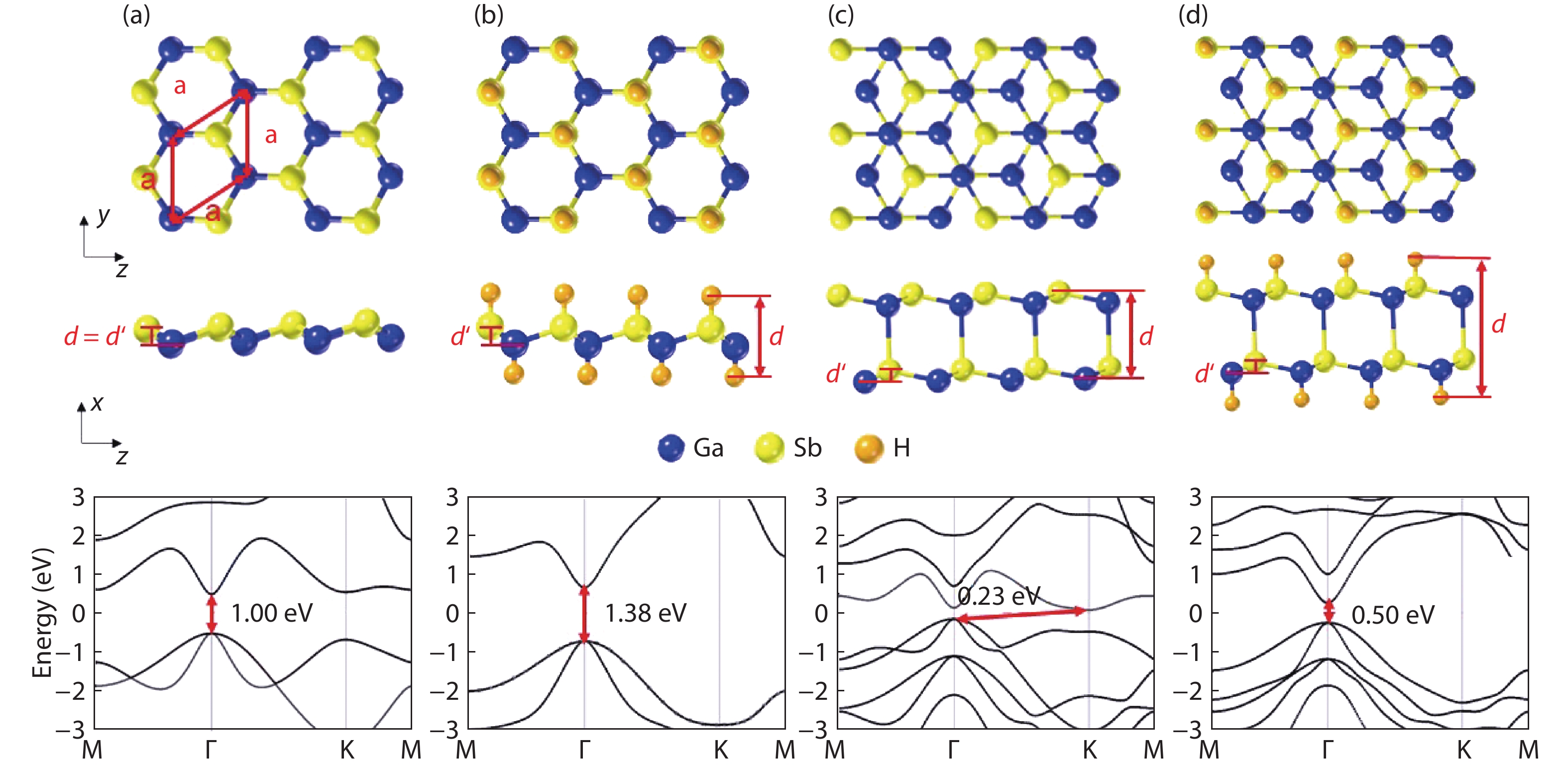
Fig. 1.
(Color online) Top and side views and band structures of (a) ML GaSb, (b) ML h-GaSb, (c) BL GaSb, and (d) BL h-GaSb.
ARTICLES
Panpan Wang, Songxuan Han and Ruge Quhe
Corresponding author: Ruge Quhe, quheruge@bupt.edu.cn
Abstract: Owing to the high carrier mobility, two-dimensional (2D) gallium antimonite (GaSb) is a promising channel material for field-effect transistors (FETs) in the post-silicon era. We investigated the ballistic performance of the 2D GaSb metal–oxide–semiconductor FETs with a 10 nm-gate-length by the ab initio quantum transport simulation. Because of the wider bandgap and better gate-control ability, the performance of the 10-nm monolayer (ML) GaSb FETs is generally superior to the bilayer counterparts, including the three-to-four orders of magnitude larger on-current. Via hydrogenation, the delay-time and power consumption can be further enhanced with magnitude up to 35% and 57%, respectively, thanks to the expanded bandgap. The 10-nm ML GaSb FETs can almost meet the International Technology Roadmap for Semiconductors (ITRS) for high-performance demands in terms of the on-state current, intrinsic delay time, and power-delay product.
Key words: 2D GaSb, 10 nm MOSFET, hydrogenation, density functional theory, quantum transport simulation
| [1] |
Frank D J. Power-constrained CMOS scaling limits. IBM J Res Dev, 2002, 46, 235 doi: 10.1147/rd.462.0235
|
| [2] |
Yan R H, Ourmazd A, Lee K F. Scaling the Si MOSFET: From bulk to SOI to bulk. IEEE Trans Electron Devices, 1992, 39, 1704 doi: 10.1109/16.141237
|
| [3] |
Hu C. FinFET and UTB: How to make very short channel MOSFETs. ECS Trans, 2013, 50, 17 doi: 10.1149/05009.0017ecst
|
| [4] |
Uchida K, Koga J, Takagi S I. Experimental study on carrier transport mechanisms in double-and single-gate ultrathin-body mosfets. IEEE International Electron Devices Meeting, 2003, 33.5.1
|
| [5] |
Uchida K, Watanabe H, Kinoshita A, et al. Experimental study on carrier transport mechanism in ultrathin-body SOI nand p-MOSFETs with SOI thickness less than 5 nm. Dig Int Electron Devices Meet, 2002, 47
|
| [6] |
Uchida K, Watanabe H, Koga J, et al. Experimental study on carrier transport mechanism in ultrathin-body SOI MOSFETs. International Conference on Simulation of Semiconductor Processes and Devices, 2003, 8
|
| [7] |
Bandurin D A, Tyurnina A V, Yu G L, et al. High electron mobility, quantum Hall effect and anomalous optical response in atomically thin InSe. Nat Nanotechnol, 2017, 12, 223 doi: 10.1038/nnano.2016.242
|
| [8] |
Li L K, Yu Y J, Ye G, et al. Black phosphorus field-effect transistors. Nat Nanotechnol, 2014, 9, 372 doi: 10.1038/nnano.2014.35
|
| [9] |
Radisavljevic B, Radenovic A, Brivio J, et al. Single-layer MoS2 transistors. Nat Nanotechnol, 2011, 6, 147 doi: 10.1038/nnano.2010.279
|
| [10] |
Schwierz F, Pezoldt J, Granzner R. Two-dimensional materials and their prospects in transistor electronics. Nanoscale, 2015, 7, 8261 doi: 10.1039/C5NR01052G
|
| [11] |
Tao L, Cinquanta E, Chiappe D, et al. Silicene field-effect transistors operating at room temperature. Nat Nanotechnol, 2015, 10, 227 doi: 10.1038/nnano.2014.325
|
| [12] |
Acun A, Poelsema B, Zandvliet H J W, et al. The instability of silicene on Ag(111). Appl Phys Lett, 2013, 103, 263119 doi: 10.1063/1.4860964
|
| [13] |
Doornbos G, Passlack M. Benchmarking of III–V n-MOSFET maturity and feasibility for future CMOS. IEEE Electron Device Lett, 2010, 31, 1110 doi: 10.1109/LED.2010.2063012
|
| [14] |
del Alamo J A, Antoniadis D A, Lin J Q, et al. Nanometer-scale III-V MOSFETs. IEEE J Electron Devices Soc, 2016, 4, 205 doi: 10.1109/JEDS.2016.2571666
|
| [15] |
Lü X, He S S, Lian H X, et al. Structural, electronic, and optical properties of pristine and bilayers of hexagonal III-V binary compounds and their hydrogenated counterparts. Appl Surf Sci, 2020, 531, 147262 doi: 10.1016/j.apsusc.2020.147262
|
| [16] |
Riel H, Wernersson L E, Hong M, et al. III-V compound semiconductor transistors — from planar to nanowire structures. MRS Bull, 2014, 39, 668 doi: 10.1557/mrs.2014.137
|
| [17] |
Bahuguna B P, Saini L K, Sharma R O, et al. Strain and electric field induced metallization in the GaX (X = N, P, As & Sb) monolayer. Physica E, 2018, 99, 236 doi: 10.1016/j.physe.2018.01.018
|
| [18] |
Low T, Rodin A S, Carvalho A, et al. Tunable optical properties of multilayer black phosphorus thin films. Phys Rev B, 2014, 90, 075434 doi: 10.1103/PhysRevB.90.075434
|
| [19] |
Brandbyge M, Mozos J L, Ordejón P, et al. Density-functional method for nonequilibrium electron transport. Phys Rev B, 2002, 65, 165401 doi: 10.1103/PhysRevB.65.165401
|
| [20] |
Soler J M, Artacho E, Gale J D, et al. The SIESTA method for ab initio order-N materials simulation. J Phys: Condens Matter, 2002, 14, 2745 doi: 10.1088/0953-8984/14/11/302
|
| [21] |
Monkhorst H J, Pack J D. Special points for Brillouin-zone integrations. Phys Rev B, 1976, 13, 5188 doi: 10.1103/PhysRevB.13.5188
|
| [22] |
Perdew J P, Burke K, Ernzerhof M. Generalized gradient approximation made simple. Phys Rev Lett, 1996, 77, 3865 doi: 10.1103/PhysRevLett.77.3865
|
| [23] |
Zhuang H L, Singh A K, Hennig R G. Computational discovery of single-layer III-V materials. Phys Rev B, 2013, 87, 165415 doi: 10.1103/PhysRevB.87.165415
|
| [24] |
Fan X F, Zheng W T, Kuo J L, et al. Structural stability of single-layer MoS2 under large strain. J Phys: Condens Matter, 2015, 27, 105401 doi: 10.1088/0953-8984/27/10/105401
|
| [25] |
Lin S S. Light-emitting two-dimensional ultrathin silicon carbide. J Phys Chem C, 2012, 116, 3951 doi: 10.1021/jp210536m
|
| [26] |
Singh A K, Zhuang H L, Hennig R G. Ab initiosynthesis of single-layer III-V materials. Phys Rev B, 2014, 89, 245431 doi: 10.1103/PhysRevB.89.245431
|
| [27] |
Schwierz F. Graphene transistors. Nat Nanotechnol, 2010, 5, 487 doi: 10.1038/nnano.2010.89
|
| [28] |
Riffe D M. Temperature dependence of silicon carrier effective masses with application to femtosecond reflectivity measurements. J Opt Soc Am B, 2002, 19, 1092 doi: 10.1364/JOSAB.19.001092
|
| [29] |
Yadav D, Nair D R. Impact of source to drain tunneling on the ballistic performance of Si, Ge, GaSb, and GeSn nanowire p-MOSFETs. IEEE J Electron Devices Soc, 2020, 8, 308 doi: 10.1109/JEDS.2020.2980633
|
| [30] |
Quhe R G, Peng X Y, Pan Y Y, et al. Can a black phosphorus Schottky barrier transistor be good enough. ACS Appl Mater Interfaces, 2017, 9, 3959 doi: 10.1021/acsami.6b14699
|
| [31] |
Sun X T, Xu L, Zhang Y, et al. Performance limit of monolayer WSe2 transistors; significantly outperform their MoS2 counterpart. ACS Appl Mater Interfaces, 2020, 12, 20633 doi: 10.1021/acsami.0c01750
|
| [32] |
Yu B, Chang L, Ahmed S, et al. FinFET scaling to 10 nm gate length. IEEE International Electron Devices Meeting, 2002, 251
|
| [33] |
Ni Z Y, Ye M, Ma J H, et al. Performance upper limit of sub-10 nm monolayer MoS2 transistors. Adv Electron Mater, 2016, 2, 1600191 doi: 10.1002/aelm.201600191
|
| [34] |
Bennett B R, Ancona M G, Boos J B, et al. Strained GaSb/AlAsSb quantum wells for p-channel field-effect transistors. J Cryst Growth, 2008, 311, 47 doi: 10.1016/j.jcrysgro.2008.10.025
|
| [35] |
Bennett B R, Chick T F, Ancona M G, et al. Enhanced hole mobility and density in GaSb quantum wells. Solid State Electron, 2013, 79, 274 doi: 10.1016/j.sse.2012.08.004
|
| [36] |
Chen Y W, Tan Z, Zhao L F, et al. Mobility enhancement of strained GaSb p-channel metal–oxide–semiconductor field-effect transistors with biaxial compressive strain. Chin Phys B, 2016, 25, 038504 doi: 10.1088/1674-1056/25/3/038504
|
| [37] |
del Alamo J A. Nanometre-scale electronics with III-V compound semiconductors. Nature, 2011, 479, 317 doi: 10.1038/nature10677
|
| [38] |
Bansal A, Paul B C, Roy K. Modeling and optimization of fringe capacitance of nanoscale DGMOS devices. IEEE Trans Electron Devices, 2005, 52, 256 doi: 10.1109/TED.2004.842713
|
| [39] |
Lacord J, Ghibaudo G, Boeuf F. Comprehensive and accurate parasitic capacitance models for two- and three-dimensional CMOS device structures. IEEE Trans Electron Devices, 2012, 59, 1332 doi: 10.1109/TED.2012.2187454
|
| [40] |
Wei L, Boeuf F, Skotnicki T, et al. Parasitic capacitances: Analytical models and impact on circuit-level performance. IEEE Trans Electron Devices, 2011, 58, 1361 doi: 10.1109/TED.2011.2121912
|
| [41] |
Vicarelli L, Vitiello M S, Coquillat D, et al. Graphene field-effect transistors as room-temperature terahertz detectors. Nat Mater, 2012, 11, 865 doi: 10.1038/nmat3417
|
| [42] |
Singh S, Thakar K, Kaushik N, et al. Performance projections for two-dimensional materials in radio-frequency applications. Phys Rev Appl, 2018, 10, 014022 doi: 10.1103/PhysRevApplied.10.014022
|
| [43] |
Prasanna Kumar S, Sandeep P, Choudhary S. Changes in transconductance (gm) and Ion/Ioff with high-K dielectrics in MX2 monolayer 10 nm channel double gate n-MOSFET. Superlattices Microstruct, 2017, 111, 642 doi: 10.1016/j.spmi.2017.07.021
|
Table 1. Structural and electronic parameters of monolayer (ML) and bilayer (BL) GaSb. h-GaSb stands for the hydrogenated layer.
| Parameter | ML GaSb | ML h-GaSb | BL GaSb | BL h-GaSb |
| a (Å) | 4.36 | 4.37 | 4.38 | 4.37 |
| d (Å) | 0.81 | 2.19 | 4.46 | 7.69 |
| d′ (Å) | 0.81 | 0.87 | 0.81 | 0.90 |
| Δ (eV) | 1.00 | 1.38 | 0.23 | 0.50 |
| me* (m0) | 0.070 | 0.081 | 0.588 | 0.086 |
| mh* (m0) | 0.485 | 0.620 | 0.685 | 0.555 |
| a: lattice parameter; d: thickness; d′: the distance between Ga and Sb atom along the direction out of the plane; Δ: bandgap; me*: the electron effective mass; mh*: the heavy-hole effective mass. m0: the free effective mass. | ||||
 DownLoad: CSV
| [1] |
Frank D J. Power-constrained CMOS scaling limits. IBM J Res Dev, 2002, 46, 235 doi: 10.1147/rd.462.0235
|
| [2] |
Yan R H, Ourmazd A, Lee K F. Scaling the Si MOSFET: From bulk to SOI to bulk. IEEE Trans Electron Devices, 1992, 39, 1704 doi: 10.1109/16.141237
|
| [3] |
Hu C. FinFET and UTB: How to make very short channel MOSFETs. ECS Trans, 2013, 50, 17 doi: 10.1149/05009.0017ecst
|
| [4] |
Uchida K, Koga J, Takagi S I. Experimental study on carrier transport mechanisms in double-and single-gate ultrathin-body mosfets. IEEE International Electron Devices Meeting, 2003, 33.5.1
|
| [5] |
Uchida K, Watanabe H, Kinoshita A, et al. Experimental study on carrier transport mechanism in ultrathin-body SOI nand p-MOSFETs with SOI thickness less than 5 nm. Dig Int Electron Devices Meet, 2002, 47
|
| [6] |
Uchida K, Watanabe H, Koga J, et al. Experimental study on carrier transport mechanism in ultrathin-body SOI MOSFETs. International Conference on Simulation of Semiconductor Processes and Devices, 2003, 8
|
| [7] |
Bandurin D A, Tyurnina A V, Yu G L, et al. High electron mobility, quantum Hall effect and anomalous optical response in atomically thin InSe. Nat Nanotechnol, 2017, 12, 223 doi: 10.1038/nnano.2016.242
|
| [8] |
Li L K, Yu Y J, Ye G, et al. Black phosphorus field-effect transistors. Nat Nanotechnol, 2014, 9, 372 doi: 10.1038/nnano.2014.35
|
| [9] |
Radisavljevic B, Radenovic A, Brivio J, et al. Single-layer MoS2 transistors. Nat Nanotechnol, 2011, 6, 147 doi: 10.1038/nnano.2010.279
|
| [10] |
Schwierz F, Pezoldt J, Granzner R. Two-dimensional materials and their prospects in transistor electronics. Nanoscale, 2015, 7, 8261 doi: 10.1039/C5NR01052G
|
| [11] |
Tao L, Cinquanta E, Chiappe D, et al. Silicene field-effect transistors operating at room temperature. Nat Nanotechnol, 2015, 10, 227 doi: 10.1038/nnano.2014.325
|
| [12] |
Acun A, Poelsema B, Zandvliet H J W, et al. The instability of silicene on Ag(111). Appl Phys Lett, 2013, 103, 263119 doi: 10.1063/1.4860964
|
| [13] |
Doornbos G, Passlack M. Benchmarking of III–V n-MOSFET maturity and feasibility for future CMOS. IEEE Electron Device Lett, 2010, 31, 1110 doi: 10.1109/LED.2010.2063012
|
| [14] |
del Alamo J A, Antoniadis D A, Lin J Q, et al. Nanometer-scale III-V MOSFETs. IEEE J Electron Devices Soc, 2016, 4, 205 doi: 10.1109/JEDS.2016.2571666
|
| [15] |
Lü X, He S S, Lian H X, et al. Structural, electronic, and optical properties of pristine and bilayers of hexagonal III-V binary compounds and their hydrogenated counterparts. Appl Surf Sci, 2020, 531, 147262 doi: 10.1016/j.apsusc.2020.147262
|
| [16] |
Riel H, Wernersson L E, Hong M, et al. III-V compound semiconductor transistors — from planar to nanowire structures. MRS Bull, 2014, 39, 668 doi: 10.1557/mrs.2014.137
|
| [17] |
Bahuguna B P, Saini L K, Sharma R O, et al. Strain and electric field induced metallization in the GaX (X = N, P, As & Sb) monolayer. Physica E, 2018, 99, 236 doi: 10.1016/j.physe.2018.01.018
|
| [18] |
Low T, Rodin A S, Carvalho A, et al. Tunable optical properties of multilayer black phosphorus thin films. Phys Rev B, 2014, 90, 075434 doi: 10.1103/PhysRevB.90.075434
|
| [19] |
Brandbyge M, Mozos J L, Ordejón P, et al. Density-functional method for nonequilibrium electron transport. Phys Rev B, 2002, 65, 165401 doi: 10.1103/PhysRevB.65.165401
|
| [20] |
Soler J M, Artacho E, Gale J D, et al. The SIESTA method for ab initio order-N materials simulation. J Phys: Condens Matter, 2002, 14, 2745 doi: 10.1088/0953-8984/14/11/302
|
| [21] |
Monkhorst H J, Pack J D. Special points for Brillouin-zone integrations. Phys Rev B, 1976, 13, 5188 doi: 10.1103/PhysRevB.13.5188
|
| [22] |
Perdew J P, Burke K, Ernzerhof M. Generalized gradient approximation made simple. Phys Rev Lett, 1996, 77, 3865 doi: 10.1103/PhysRevLett.77.3865
|
| [23] |
Zhuang H L, Singh A K, Hennig R G. Computational discovery of single-layer III-V materials. Phys Rev B, 2013, 87, 165415 doi: 10.1103/PhysRevB.87.165415
|
| [24] |
Fan X F, Zheng W T, Kuo J L, et al. Structural stability of single-layer MoS2 under large strain. J Phys: Condens Matter, 2015, 27, 105401 doi: 10.1088/0953-8984/27/10/105401
|
| [25] |
Lin S S. Light-emitting two-dimensional ultrathin silicon carbide. J Phys Chem C, 2012, 116, 3951 doi: 10.1021/jp210536m
|
| [26] |
Singh A K, Zhuang H L, Hennig R G. Ab initiosynthesis of single-layer III-V materials. Phys Rev B, 2014, 89, 245431 doi: 10.1103/PhysRevB.89.245431
|
| [27] |
Schwierz F. Graphene transistors. Nat Nanotechnol, 2010, 5, 487 doi: 10.1038/nnano.2010.89
|
| [28] |
Riffe D M. Temperature dependence of silicon carrier effective masses with application to femtosecond reflectivity measurements. J Opt Soc Am B, 2002, 19, 1092 doi: 10.1364/JOSAB.19.001092
|
| [29] |
Yadav D, Nair D R. Impact of source to drain tunneling on the ballistic performance of Si, Ge, GaSb, and GeSn nanowire p-MOSFETs. IEEE J Electron Devices Soc, 2020, 8, 308 doi: 10.1109/JEDS.2020.2980633
|
| [30] |
Quhe R G, Peng X Y, Pan Y Y, et al. Can a black phosphorus Schottky barrier transistor be good enough. ACS Appl Mater Interfaces, 2017, 9, 3959 doi: 10.1021/acsami.6b14699
|
| [31] |
Sun X T, Xu L, Zhang Y, et al. Performance limit of monolayer WSe2 transistors; significantly outperform their MoS2 counterpart. ACS Appl Mater Interfaces, 2020, 12, 20633 doi: 10.1021/acsami.0c01750
|
| [32] |
Yu B, Chang L, Ahmed S, et al. FinFET scaling to 10 nm gate length. IEEE International Electron Devices Meeting, 2002, 251
|
| [33] |
Ni Z Y, Ye M, Ma J H, et al. Performance upper limit of sub-10 nm monolayer MoS2 transistors. Adv Electron Mater, 2016, 2, 1600191 doi: 10.1002/aelm.201600191
|
| [34] |
Bennett B R, Ancona M G, Boos J B, et al. Strained GaSb/AlAsSb quantum wells for p-channel field-effect transistors. J Cryst Growth, 2008, 311, 47 doi: 10.1016/j.jcrysgro.2008.10.025
|
| [35] |
Bennett B R, Chick T F, Ancona M G, et al. Enhanced hole mobility and density in GaSb quantum wells. Solid State Electron, 2013, 79, 274 doi: 10.1016/j.sse.2012.08.004
|
| [36] |
Chen Y W, Tan Z, Zhao L F, et al. Mobility enhancement of strained GaSb p-channel metal–oxide–semiconductor field-effect transistors with biaxial compressive strain. Chin Phys B, 2016, 25, 038504 doi: 10.1088/1674-1056/25/3/038504
|
| [37] |
del Alamo J A. Nanometre-scale electronics with III-V compound semiconductors. Nature, 2011, 479, 317 doi: 10.1038/nature10677
|
| [38] |
Bansal A, Paul B C, Roy K. Modeling and optimization of fringe capacitance of nanoscale DGMOS devices. IEEE Trans Electron Devices, 2005, 52, 256 doi: 10.1109/TED.2004.842713
|
| [39] |
Lacord J, Ghibaudo G, Boeuf F. Comprehensive and accurate parasitic capacitance models for two- and three-dimensional CMOS device structures. IEEE Trans Electron Devices, 2012, 59, 1332 doi: 10.1109/TED.2012.2187454
|
| [40] |
Wei L, Boeuf F, Skotnicki T, et al. Parasitic capacitances: Analytical models and impact on circuit-level performance. IEEE Trans Electron Devices, 2011, 58, 1361 doi: 10.1109/TED.2011.2121912
|
| [41] |
Vicarelli L, Vitiello M S, Coquillat D, et al. Graphene field-effect transistors as room-temperature terahertz detectors. Nat Mater, 2012, 11, 865 doi: 10.1038/nmat3417
|
| [42] |
Singh S, Thakar K, Kaushik N, et al. Performance projections for two-dimensional materials in radio-frequency applications. Phys Rev Appl, 2018, 10, 014022 doi: 10.1103/PhysRevApplied.10.014022
|
| [43] |
Prasanna Kumar S, Sandeep P, Choudhary S. Changes in transconductance (gm) and Ion/Ioff with high-K dielectrics in MX2 monolayer 10 nm channel double gate n-MOSFET. Superlattices Microstruct, 2017, 111, 642 doi: 10.1016/j.spmi.2017.07.021
|


Article views: 2062 Times PDF downloads: 93 Times Cited by: 0 Times
Received: 27 April 2021 Revised: 29 May 2021 Online: Accepted Manuscript: 05 July 2021Uncorrected proof: 06 July 2021Published: 03 December 2021
| Citation: |
Panpan Wang, Songxuan Han, Ruge Quhe. Quantum transport simulation of the two-dimensional GaSb transistors[J]. Journal of Semiconductors, 2021, 42(12): 122001. doi: 10.1088/1674-4926/42/12/122001
P P Wang, S X Han, R G Quhe, Quantum transport simulation of the two-dimensional GaSb transistors[J]. J. Semicond., 2021, 42(12): 122001. doi: 10.1088/1674-4926/42/12/122001.
Export: BibTex EndNote

|
| [1] |
Frank D J. Power-constrained CMOS scaling limits. IBM J Res Dev, 2002, 46, 235 doi: 10.1147/rd.462.0235
|
| [2] |
Yan R H, Ourmazd A, Lee K F. Scaling the Si MOSFET: From bulk to SOI to bulk. IEEE Trans Electron Devices, 1992, 39, 1704 doi: 10.1109/16.141237
|
| [3] |
Hu C. FinFET and UTB: How to make very short channel MOSFETs. ECS Trans, 2013, 50, 17 doi: 10.1149/05009.0017ecst
|
| [4] |
Uchida K, Koga J, Takagi S I. Experimental study on carrier transport mechanisms in double-and single-gate ultrathin-body mosfets. IEEE International Electron Devices Meeting, 2003, 33.5.1
|
| [5] |
Uchida K, Watanabe H, Kinoshita A, et al. Experimental study on carrier transport mechanism in ultrathin-body SOI nand p-MOSFETs with SOI thickness less than 5 nm. Dig Int Electron Devices Meet, 2002, 47
|
| [6] |
Uchida K, Watanabe H, Koga J, et al. Experimental study on carrier transport mechanism in ultrathin-body SOI MOSFETs. International Conference on Simulation of Semiconductor Processes and Devices, 2003, 8
|
| [7] |
Bandurin D A, Tyurnina A V, Yu G L, et al. High electron mobility, quantum Hall effect and anomalous optical response in atomically thin InSe. Nat Nanotechnol, 2017, 12, 223 doi: 10.1038/nnano.2016.242
|
| [8] |
Li L K, Yu Y J, Ye G, et al. Black phosphorus field-effect transistors. Nat Nanotechnol, 2014, 9, 372 doi: 10.1038/nnano.2014.35
|
| [9] |
Radisavljevic B, Radenovic A, Brivio J, et al. Single-layer MoS2 transistors. Nat Nanotechnol, 2011, 6, 147 doi: 10.1038/nnano.2010.279
|
| [10] |
Schwierz F, Pezoldt J, Granzner R. Two-dimensional materials and their prospects in transistor electronics. Nanoscale, 2015, 7, 8261 doi: 10.1039/C5NR01052G
|
| [11] |
Tao L, Cinquanta E, Chiappe D, et al. Silicene field-effect transistors operating at room temperature. Nat Nanotechnol, 2015, 10, 227 doi: 10.1038/nnano.2014.325
|
| [12] |
Acun A, Poelsema B, Zandvliet H J W, et al. The instability of silicene on Ag(111). Appl Phys Lett, 2013, 103, 263119 doi: 10.1063/1.4860964
|
| [13] |
Doornbos G, Passlack M. Benchmarking of III–V n-MOSFET maturity and feasibility for future CMOS. IEEE Electron Device Lett, 2010, 31, 1110 doi: 10.1109/LED.2010.2063012
|
| [14] |
del Alamo J A, Antoniadis D A, Lin J Q, et al. Nanometer-scale III-V MOSFETs. IEEE J Electron Devices Soc, 2016, 4, 205 doi: 10.1109/JEDS.2016.2571666
|
| [15] |
Lü X, He S S, Lian H X, et al. Structural, electronic, and optical properties of pristine and bilayers of hexagonal III-V binary compounds and their hydrogenated counterparts. Appl Surf Sci, 2020, 531, 147262 doi: 10.1016/j.apsusc.2020.147262
|
| [16] |
Riel H, Wernersson L E, Hong M, et al. III-V compound semiconductor transistors — from planar to nanowire structures. MRS Bull, 2014, 39, 668 doi: 10.1557/mrs.2014.137
|
| [17] |
Bahuguna B P, Saini L K, Sharma R O, et al. Strain and electric field induced metallization in the GaX (X = N, P, As & Sb) monolayer. Physica E, 2018, 99, 236 doi: 10.1016/j.physe.2018.01.018
|
| [18] |
Low T, Rodin A S, Carvalho A, et al. Tunable optical properties of multilayer black phosphorus thin films. Phys Rev B, 2014, 90, 075434 doi: 10.1103/PhysRevB.90.075434
|
| [19] |
Brandbyge M, Mozos J L, Ordejón P, et al. Density-functional method for nonequilibrium electron transport. Phys Rev B, 2002, 65, 165401 doi: 10.1103/PhysRevB.65.165401
|
| [20] |
Soler J M, Artacho E, Gale J D, et al. The SIESTA method for ab initio order-N materials simulation. J Phys: Condens Matter, 2002, 14, 2745 doi: 10.1088/0953-8984/14/11/302
|
| [21] |
Monkhorst H J, Pack J D. Special points for Brillouin-zone integrations. Phys Rev B, 1976, 13, 5188 doi: 10.1103/PhysRevB.13.5188
|
| [22] |
Perdew J P, Burke K, Ernzerhof M. Generalized gradient approximation made simple. Phys Rev Lett, 1996, 77, 3865 doi: 10.1103/PhysRevLett.77.3865
|
| [23] |
Zhuang H L, Singh A K, Hennig R G. Computational discovery of single-layer III-V materials. Phys Rev B, 2013, 87, 165415 doi: 10.1103/PhysRevB.87.165415
|
| [24] |
Fan X F, Zheng W T, Kuo J L, et al. Structural stability of single-layer MoS2 under large strain. J Phys: Condens Matter, 2015, 27, 105401 doi: 10.1088/0953-8984/27/10/105401
|
| [25] |
Lin S S. Light-emitting two-dimensional ultrathin silicon carbide. J Phys Chem C, 2012, 116, 3951 doi: 10.1021/jp210536m
|
| [26] |
Singh A K, Zhuang H L, Hennig R G. Ab initiosynthesis of single-layer III-V materials. Phys Rev B, 2014, 89, 245431 doi: 10.1103/PhysRevB.89.245431
|
| [27] |
Schwierz F. Graphene transistors. Nat Nanotechnol, 2010, 5, 487 doi: 10.1038/nnano.2010.89
|
| [28] |
Riffe D M. Temperature dependence of silicon carrier effective masses with application to femtosecond reflectivity measurements. J Opt Soc Am B, 2002, 19, 1092 doi: 10.1364/JOSAB.19.001092
|
| [29] |
Yadav D, Nair D R. Impact of source to drain tunneling on the ballistic performance of Si, Ge, GaSb, and GeSn nanowire p-MOSFETs. IEEE J Electron Devices Soc, 2020, 8, 308 doi: 10.1109/JEDS.2020.2980633
|
| [30] |
Quhe R G, Peng X Y, Pan Y Y, et al. Can a black phosphorus Schottky barrier transistor be good enough. ACS Appl Mater Interfaces, 2017, 9, 3959 doi: 10.1021/acsami.6b14699
|
| [31] |
Sun X T, Xu L, Zhang Y, et al. Performance limit of monolayer WSe2 transistors; significantly outperform their MoS2 counterpart. ACS Appl Mater Interfaces, 2020, 12, 20633 doi: 10.1021/acsami.0c01750
|
| [32] |
Yu B, Chang L, Ahmed S, et al. FinFET scaling to 10 nm gate length. IEEE International Electron Devices Meeting, 2002, 251
|
| [33] |
Ni Z Y, Ye M, Ma J H, et al. Performance upper limit of sub-10 nm monolayer MoS2 transistors. Adv Electron Mater, 2016, 2, 1600191 doi: 10.1002/aelm.201600191
|
| [34] |
Bennett B R, Ancona M G, Boos J B, et al. Strained GaSb/AlAsSb quantum wells for p-channel field-effect transistors. J Cryst Growth, 2008, 311, 47 doi: 10.1016/j.jcrysgro.2008.10.025
|
| [35] |
Bennett B R, Chick T F, Ancona M G, et al. Enhanced hole mobility and density in GaSb quantum wells. Solid State Electron, 2013, 79, 274 doi: 10.1016/j.sse.2012.08.004
|
| [36] |
Chen Y W, Tan Z, Zhao L F, et al. Mobility enhancement of strained GaSb p-channel metal–oxide–semiconductor field-effect transistors with biaxial compressive strain. Chin Phys B, 2016, 25, 038504 doi: 10.1088/1674-1056/25/3/038504
|
| [37] |
del Alamo J A. Nanometre-scale electronics with III-V compound semiconductors. Nature, 2011, 479, 317 doi: 10.1038/nature10677
|
| [38] |
Bansal A, Paul B C, Roy K. Modeling and optimization of fringe capacitance of nanoscale DGMOS devices. IEEE Trans Electron Devices, 2005, 52, 256 doi: 10.1109/TED.2004.842713
|
| [39] |
Lacord J, Ghibaudo G, Boeuf F. Comprehensive and accurate parasitic capacitance models for two- and three-dimensional CMOS device structures. IEEE Trans Electron Devices, 2012, 59, 1332 doi: 10.1109/TED.2012.2187454
|
| [40] |
Wei L, Boeuf F, Skotnicki T, et al. Parasitic capacitances: Analytical models and impact on circuit-level performance. IEEE Trans Electron Devices, 2011, 58, 1361 doi: 10.1109/TED.2011.2121912
|
| [41] |
Vicarelli L, Vitiello M S, Coquillat D, et al. Graphene field-effect transistors as room-temperature terahertz detectors. Nat Mater, 2012, 11, 865 doi: 10.1038/nmat3417
|
| [42] |
Singh S, Thakar K, Kaushik N, et al. Performance projections for two-dimensional materials in radio-frequency applications. Phys Rev Appl, 2018, 10, 014022 doi: 10.1103/PhysRevApplied.10.014022
|
| [43] |
Prasanna Kumar S, Sandeep P, Choudhary S. Changes in transconductance (gm) and Ion/Ioff with high-K dielectrics in MX2 monolayer 10 nm channel double gate n-MOSFET. Superlattices Microstruct, 2017, 111, 642 doi: 10.1016/j.spmi.2017.07.021
|

 WeChat ID
Journal of Semiconductors © 2017 All Rights Reserved 京ICP备05085259号-2


