Fig. 1.
Effect of gas composition on etching rate and surface roughness.
ARTICLES
Yongkang Xu1, 2, Sannian Song1, , Wencheng Fang1, 2, Chengxing Li1, 2 and Zhitang Song1
Corresponding author: Sannian Song, songsannian@mail.sim.ac.cn
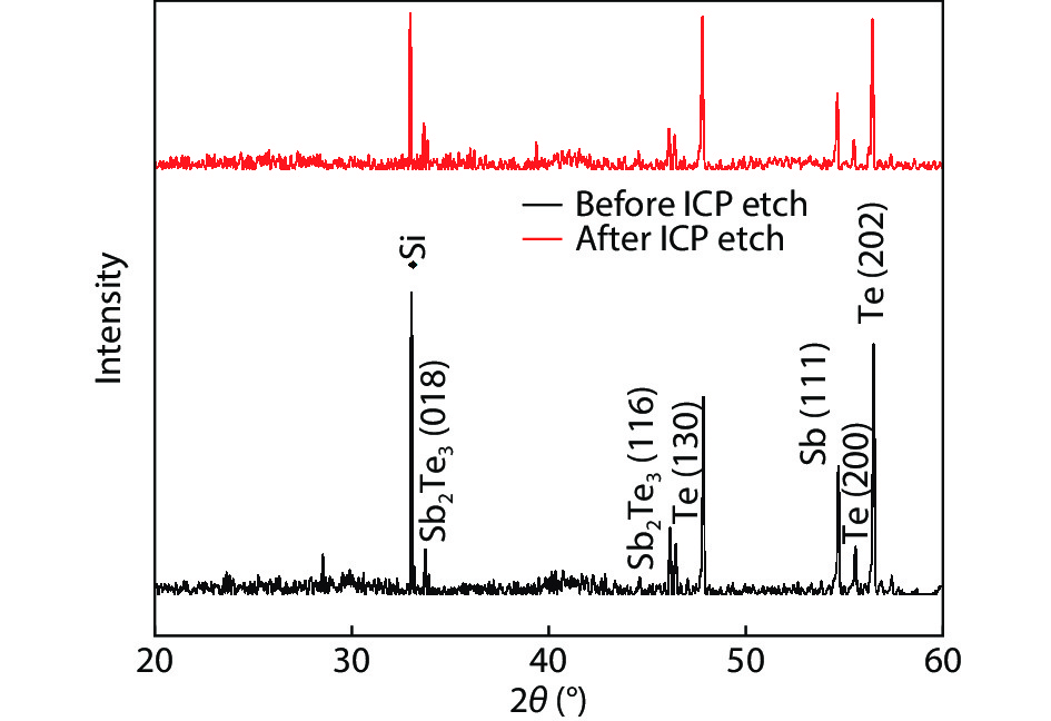
Abstract: Compared to the conventional phase change materials, the new phase change material Ta-Sb2Te3 has the advantages of excellent data retention and good material stability. In this letter, the etching characteristics of Ta-Sb2Te3 were studied by using CF4/Ar. The results showed that when CF4/Ar = 25/25, the etching power was 600 W and the etching pressure was 2.5 Pa, the etching speed was up to 61 nm/min. The etching pattern of Ta-Sb2Te3 film had a smooth side wall and good perpendicularity (close to 90°), smooth surface of the etching (RMS was 0.51nm), and the etching uniformity was fine. Furthermore, the mechanism of this etching process was analyzed by X-ray photoelectron spectroscopy (XPS). The main damage mechanism of ICP etching in CF4/Ar was studied by X-ray diffraction (XRD).
Key words: new phase change material, inductively couple plasma, etching process, etching characteristics, mechanism
| [1] |
Ovshinsky S R. Reversible electrical switching phenomena in disordered structures. Phys Rev Lett, 1968, 21, 1450 doi: 10.1103/PhysRevLett.21.1450
|
| [2] |
Washington J S, Joseph E A, Raoux S, et al. Characterizing the effects of etch-induced material modification on the crystallization properties of nitrogen doped Ge2Sb2Te5. J Appl Phys, 2011, 109, 034502 doi: 10.1063/1.3524510
|
| [3] |
Xu C, Liu B, Song Z T, et al. Reactive-ion etching of Sn-doped Ge2Sb2Te5 in CHF3/O2 plasma for non-volatile phase-change memory device. Thin Solid Films, 2008, 516, 7871 doi: 10.1016/j.tsf.2008.05.039
|
| [4] |
Song Z T, Song S N, Zhu M, et al. From octahedral structure motif to sub-nanosecond phase transitions in phase change materials for data storage. Sci China Inf Sci, 2018, 61, 081302 doi: 10.1007/s11432-018-9404-2
|
| [5] |
Rao F, Song Z T, Ren K, et al. Si–Sb–Te materials for phase change memory applications. Nanotechnology, 2011, 22, 145702 doi: 10.1088/0957-4484/22/14/145702
|
| [6] |
Li J T, Xia Y Y, Liu B, et al. Direct evidence of reactive ion etching induced damages in Ge2Sb2Te5 based on different halogen plasmas. Appl Surf Sci, 2016, 378, 163 doi: 10.1016/j.apsusc.2016.03.122
|
| [7] |
Li J T, Xia Y Y, Liu B, et al. Etch characteristics and mechanism of TiSbTe thin films in inductively-coupled HBr-He, Ar, N2, O2 plasma. ECS J Solid State Sci Technol, 2016, 5, P330 doi: 10.1149/2.0201606jss
|
| [8] |
Shen L L, Song S N, Zhang Z H, et al. Characteristics and mechanism of phase change material W0.03Sb2Te etched by Cl2/BCl3 inductively coupled plasmas. Thin Solid Films, 2015, 593, 67 doi: 10.1016/j.tsf.2015.09.032
|
| [9] |
Zhang Z H, Song S N, Song Z T, et al. Characteristics and mechanism of Al1.3Sb3Te etched by Cl2/BCl3 inductively coupled plasmas. Microelectron Eng, 2014, 115, 51 doi: 10.1016/j.mee.2013.10.016
|
| [10] |
Kang S K, Jeon M H, Park J Y, et al. Etch damage of Ge2Sb2Te5 for different halogen gases. Jpn J Appl Phys, 2011, 50, 086501 doi: 10.1143/JJAP.50.086501
|
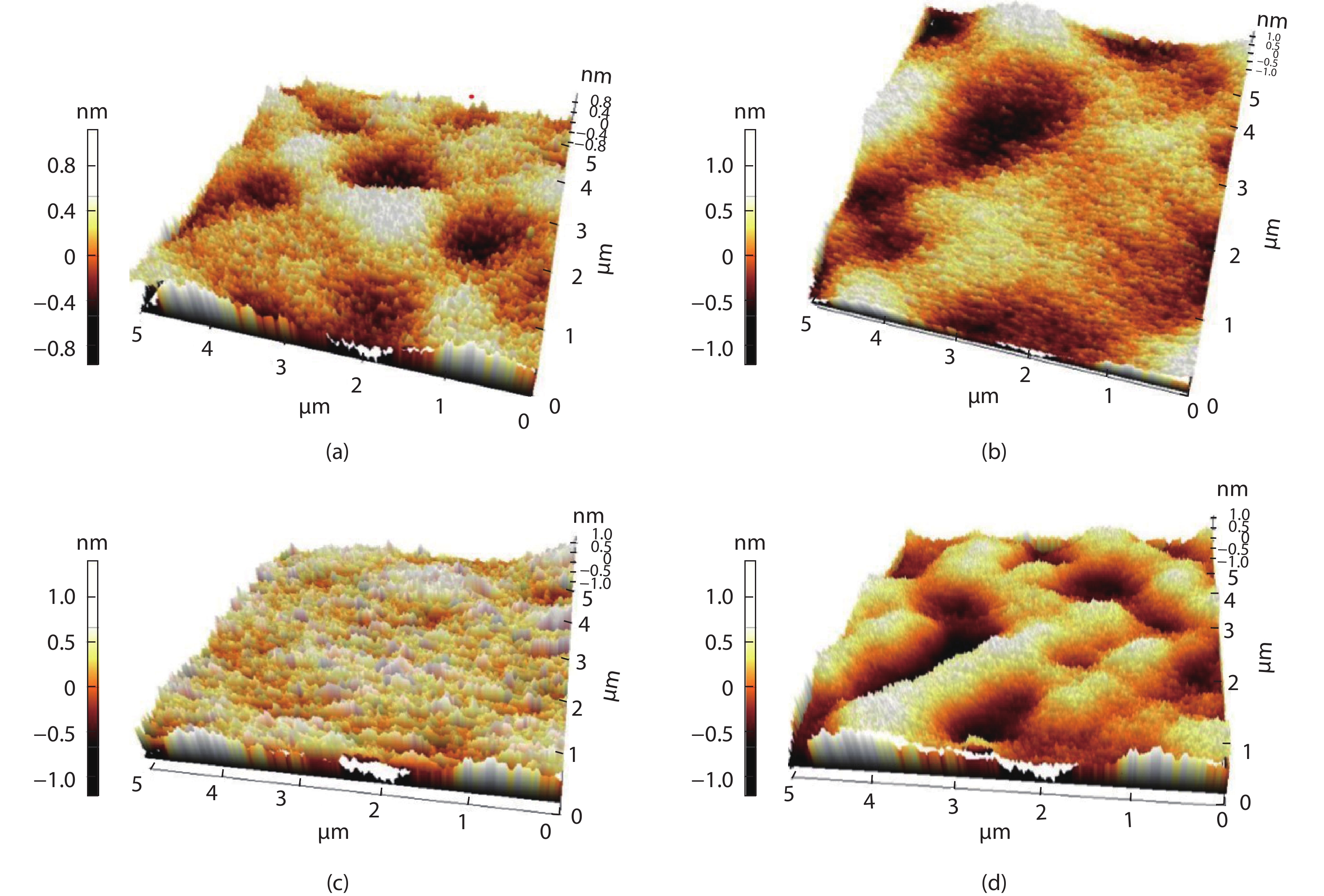
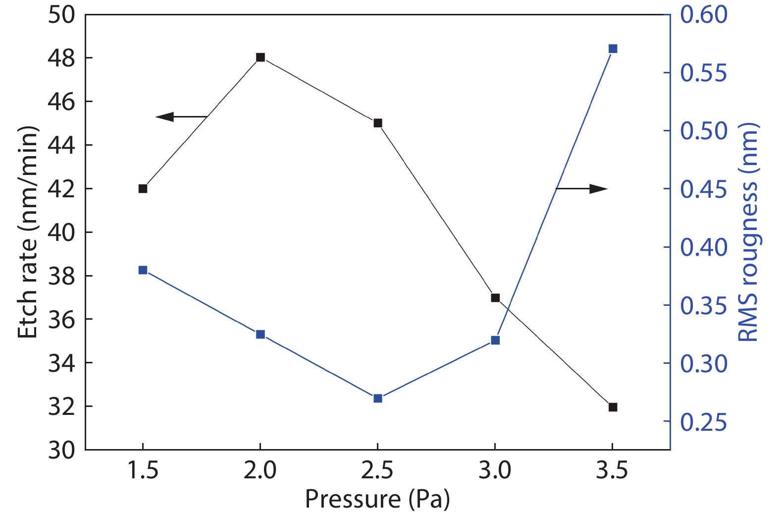
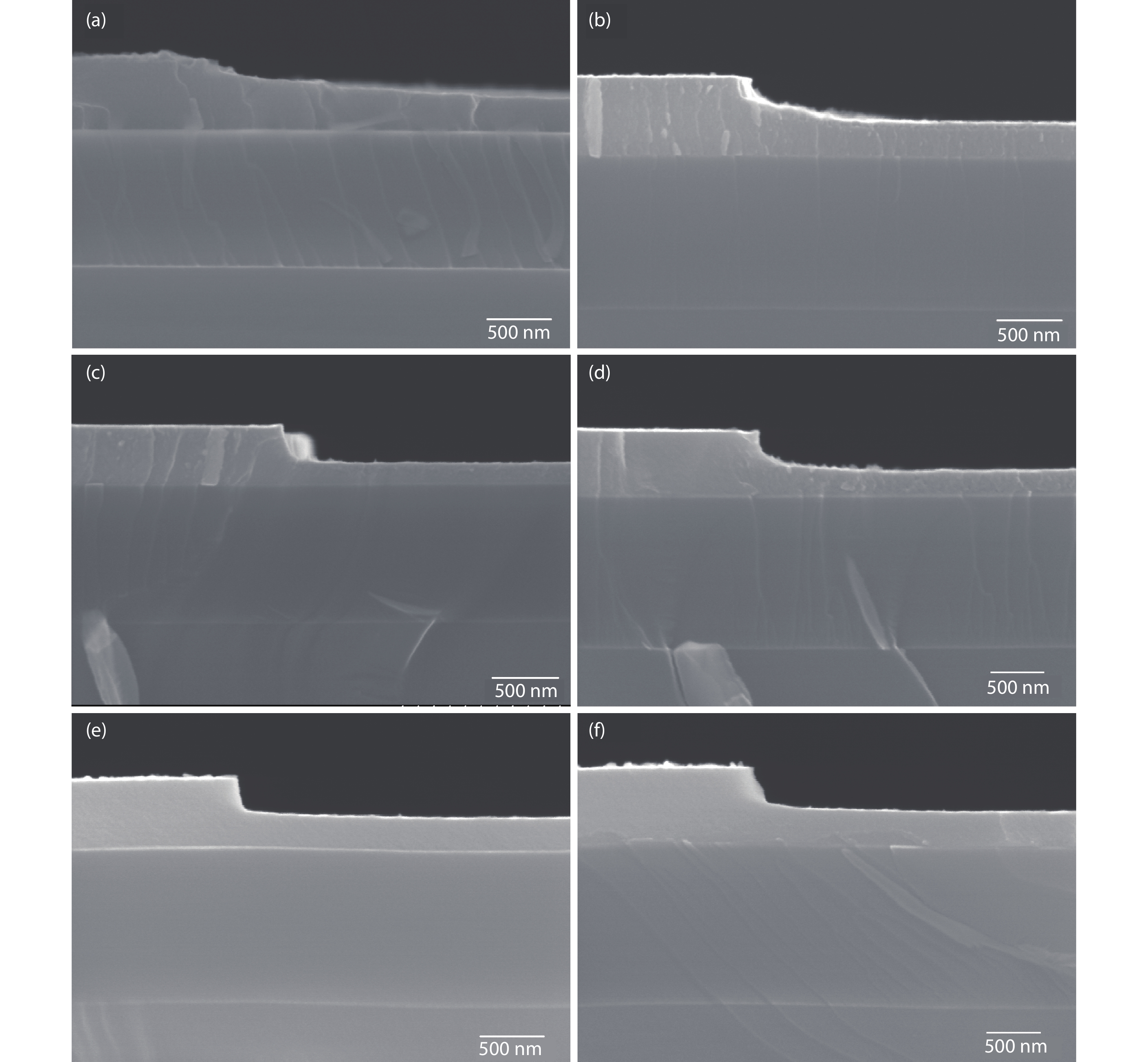
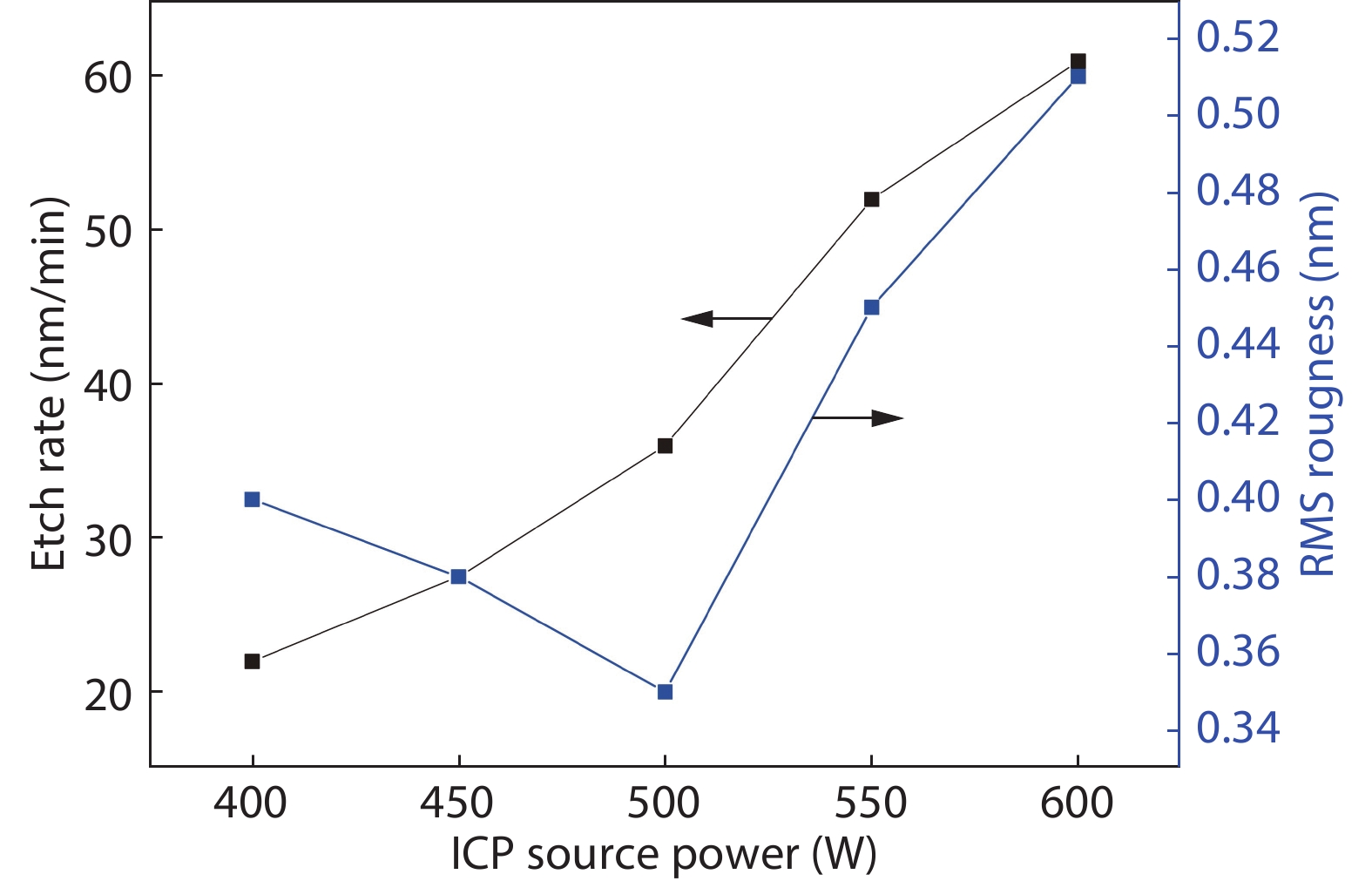

Table 1. The boiling point of fluoride.
| Element | Chemical compound | Boiling point (°C) |
| Sb | SbF5 | 141 |
| Sb | SbF3 | 345 |
| Te | TeF4 | 195 |
| Te | TeF6 | –39 |
 DownLoad: CSV
| [1] |
Ovshinsky S R. Reversible electrical switching phenomena in disordered structures. Phys Rev Lett, 1968, 21, 1450 doi: 10.1103/PhysRevLett.21.1450
|
| [2] |
Washington J S, Joseph E A, Raoux S, et al. Characterizing the effects of etch-induced material modification on the crystallization properties of nitrogen doped Ge2Sb2Te5. J Appl Phys, 2011, 109, 034502 doi: 10.1063/1.3524510
|
| [3] |
Xu C, Liu B, Song Z T, et al. Reactive-ion etching of Sn-doped Ge2Sb2Te5 in CHF3/O2 plasma for non-volatile phase-change memory device. Thin Solid Films, 2008, 516, 7871 doi: 10.1016/j.tsf.2008.05.039
|
| [4] |
Song Z T, Song S N, Zhu M, et al. From octahedral structure motif to sub-nanosecond phase transitions in phase change materials for data storage. Sci China Inf Sci, 2018, 61, 081302 doi: 10.1007/s11432-018-9404-2
|
| [5] |
Rao F, Song Z T, Ren K, et al. Si–Sb–Te materials for phase change memory applications. Nanotechnology, 2011, 22, 145702 doi: 10.1088/0957-4484/22/14/145702
|
| [6] |
Li J T, Xia Y Y, Liu B, et al. Direct evidence of reactive ion etching induced damages in Ge2Sb2Te5 based on different halogen plasmas. Appl Surf Sci, 2016, 378, 163 doi: 10.1016/j.apsusc.2016.03.122
|
| [7] |
Li J T, Xia Y Y, Liu B, et al. Etch characteristics and mechanism of TiSbTe thin films in inductively-coupled HBr-He, Ar, N2, O2 plasma. ECS J Solid State Sci Technol, 2016, 5, P330 doi: 10.1149/2.0201606jss
|
| [8] |
Shen L L, Song S N, Zhang Z H, et al. Characteristics and mechanism of phase change material W0.03Sb2Te etched by Cl2/BCl3 inductively coupled plasmas. Thin Solid Films, 2015, 593, 67 doi: 10.1016/j.tsf.2015.09.032
|
| [9] |
Zhang Z H, Song S N, Song Z T, et al. Characteristics and mechanism of Al1.3Sb3Te etched by Cl2/BCl3 inductively coupled plasmas. Microelectron Eng, 2014, 115, 51 doi: 10.1016/j.mee.2013.10.016
|
| [10] |
Kang S K, Jeon M H, Park J Y, et al. Etch damage of Ge2Sb2Te5 for different halogen gases. Jpn J Appl Phys, 2011, 50, 086501 doi: 10.1143/JJAP.50.086501
|


Article views: 5157 Times PDF downloads: 68 Times Cited by: 0 Times
Received: 22 April 2020 Revised: 26 May 2020 Online: Accepted Manuscript: 11 August 2020Uncorrected proof: 19 August 2020Published: 08 December 2020
| Citation: |
Yongkang Xu, Sannian Song, Wencheng Fang, Chengxing Li, Zhitang Song. The etching process and mechanism analysis of Ta-Sb2Te3 film based on inductively coupled plasma[J]. Journal of Semiconductors, 2020, 41(12): 122103. doi: 10.1088/1674-4926/41/12/122103
****
Y K Xu, S N Song, W C Fang, C X Li, Z T Song, The etching process and mechanism analysis of Ta-Sb2Te3 film based on inductively coupled plasma[J]. J. Semicond., 2020, 41(12): 122103. doi: 10.1088/1674-4926/41/12/122103.

|
| [1] |
Ovshinsky S R. Reversible electrical switching phenomena in disordered structures. Phys Rev Lett, 1968, 21, 1450 doi: 10.1103/PhysRevLett.21.1450
|
| [2] |
Washington J S, Joseph E A, Raoux S, et al. Characterizing the effects of etch-induced material modification on the crystallization properties of nitrogen doped Ge2Sb2Te5. J Appl Phys, 2011, 109, 034502 doi: 10.1063/1.3524510
|
| [3] |
Xu C, Liu B, Song Z T, et al. Reactive-ion etching of Sn-doped Ge2Sb2Te5 in CHF3/O2 plasma for non-volatile phase-change memory device. Thin Solid Films, 2008, 516, 7871 doi: 10.1016/j.tsf.2008.05.039
|
| [4] |
Song Z T, Song S N, Zhu M, et al. From octahedral structure motif to sub-nanosecond phase transitions in phase change materials for data storage. Sci China Inf Sci, 2018, 61, 081302 doi: 10.1007/s11432-018-9404-2
|
| [5] |
Rao F, Song Z T, Ren K, et al. Si–Sb–Te materials for phase change memory applications. Nanotechnology, 2011, 22, 145702 doi: 10.1088/0957-4484/22/14/145702
|
| [6] |
Li J T, Xia Y Y, Liu B, et al. Direct evidence of reactive ion etching induced damages in Ge2Sb2Te5 based on different halogen plasmas. Appl Surf Sci, 2016, 378, 163 doi: 10.1016/j.apsusc.2016.03.122
|
| [7] |
Li J T, Xia Y Y, Liu B, et al. Etch characteristics and mechanism of TiSbTe thin films in inductively-coupled HBr-He, Ar, N2, O2 plasma. ECS J Solid State Sci Technol, 2016, 5, P330 doi: 10.1149/2.0201606jss
|
| [8] |
Shen L L, Song S N, Zhang Z H, et al. Characteristics and mechanism of phase change material W0.03Sb2Te etched by Cl2/BCl3 inductively coupled plasmas. Thin Solid Films, 2015, 593, 67 doi: 10.1016/j.tsf.2015.09.032
|
| [9] |
Zhang Z H, Song S N, Song Z T, et al. Characteristics and mechanism of Al1.3Sb3Te etched by Cl2/BCl3 inductively coupled plasmas. Microelectron Eng, 2014, 115, 51 doi: 10.1016/j.mee.2013.10.016
|
| [10] |
Kang S K, Jeon M H, Park J Y, et al. Etch damage of Ge2Sb2Te5 for different halogen gases. Jpn J Appl Phys, 2011, 50, 086501 doi: 10.1143/JJAP.50.086501
|

 WeChat ID
Journal of Semiconductors © 2017 All Rights Reserved 京ICP备05085259号-2