


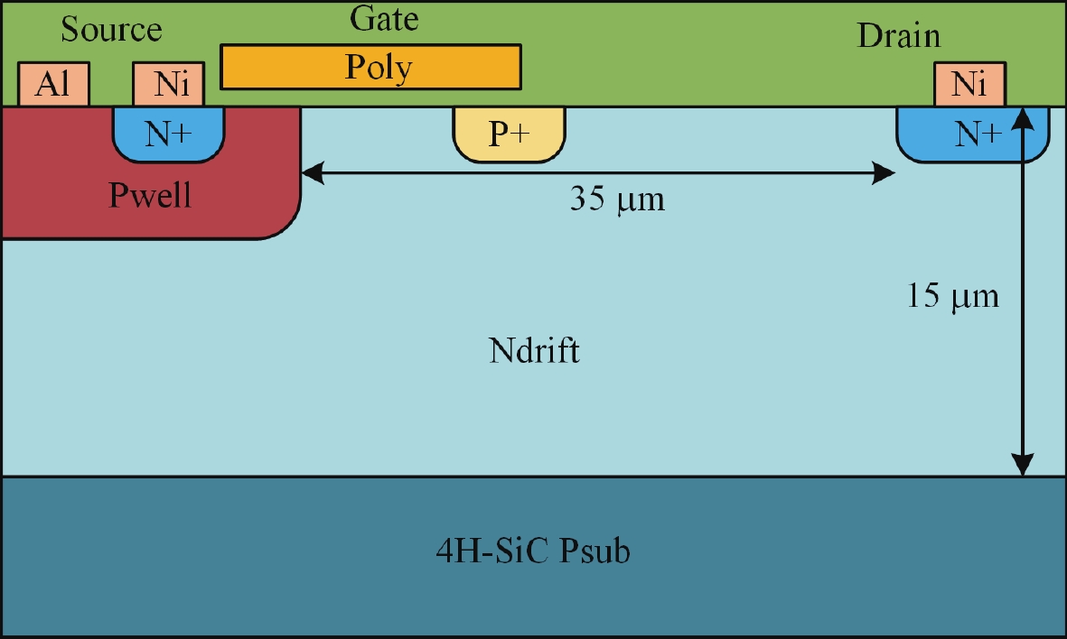
Fig. 1.
(Color online) Device diagram of the first fabricated 4H-SiC LDMOS power device.
REVIEWS
Ziwei Hu1, 2, 3, §, Jiafei Yao1, 2, 3, §, , Ang Li1, 2, 3, Qi Sun1, 2, 3, Man Li1, 2, Kemeng Yang1, 2, Jun Zhang1, 2, Jing Chen1, 2, Maolin Zhang1, 2 and Yufeng Guo1, 2,
Corresponding author: Jiafei Yao, jfyao@njupt.edu.cn; Yufeng Guo, yfguo@njupt.edu.cn
Abstract: Silicon carbide (SiC), as a third-generation semiconductor material, possesses exceptional material properties that significantly enhance the performance of power devices. The SiC lateral double-diffused metal–oxide–semiconductor (LDMOS) power devices have undergone continuous optimization, resulting in an increase in breakdown voltage (BV) and ultra-low specific on-resistance (Ron,sp). This paper has summarized the structural optimizations and experimental progress of SiC LDMOS power devices, including the trench-gate technology, reduced surface field (RESURF) technology, doping technology, junction termination techniques and so on. The paper is aimed at enhancing the understanding of the operational mechanisms and providing guidelines for the further development of SiC LDMOS power devices.
Keywords: SiC, LDMOS, specific on-resistance, breakdown voltage
| [1] |
Li J Y, Zhao Y M, Liu X F, et al. Uniformity investigation in 3C-SiC epitaxial layers grown on Si substrates by horizontal hot-wall CVD. J Semicond, 2006, 28(1), 1
|
| [2] |
Yan G G, Sun G S, Wu H L, et al. Multi-wafer 3C-SiC thin films grown on Si (100) in a vertical HWLPCVD reactor. J Semicond, 2011, 32(6), 063001 doi: 10.1088/1674-4926/32/6/063001
|
| [3] |
Liu M, Yang Y, Mao Q, et al. Influence of radio frequency magnetron sputtering parameters on the structure and performance of SiC films. Ceram Int, 2021, 47(17), 24098 doi: 10.1016/j.ceramint.2021.05.120
|
| [4] |
Pelt J S, Ramsey M E, Durbin S M. Characterization of crystalline SiC films grown by pulsed laser deposition. Thin Solid Films, 2000, 371(1-2), 72 doi: 10.1016/S0040-6090(00)00991-3
|
| [5] |
Nishino S, Powell J A, Will H A. Production of large-area single-crystal wafers of cubic SiC for semiconductor devices. Appl Phys Lett, 1983, 42(5), 460 doi: 10.1063/1.93970
|
| [6] |
Powell J A, Matus L G, Kuczmarski M A. Growth and characterization of cubic SiC single-crystal films on Si. J Electrochem Soc, 1987, 134(6), 1558 doi: 10.1149/1.2100708
|
| [7] |
Ning P Q, Yuan T S, Kang Y H, et al. Review of Si IGBT and SiC MOSFET based on hybrid switch. Chin J Electr Eng, 2019, 5(3), 20 doi: 10.23919/CJEE.2019.000017
|
| [8] |
Kaur R, Gupta P, Singh J. A review on power MOSFET device structures. Int J Res Appl Sci Eng Technol, 2017, 5(X), 208 doi: 10.22214/IJRASET.2017.10034
|
| [9] |
Spitz J, Melloch M R, Cooper J A, et al. 2.6 kV 4H-SiC lateral DMOSFETs. IEEE Electron Device Lett, 1998, 19(4), 100 doi: 10.1109/55.663527
|
| [10] |
Chen G, Bai S, Zhang T, et al. 4H-SiC MESFET device process. J Semicond, 2007, 28(S1), 565
|
| [11] |
Kukushkin S A, Osipov A V, Feoktistov N A. Synthesis of epitaxial silicon carbide films through the substitution of atoms in the silicon crystal lattice: A review. Phys Solid State, 2014, 56(8), 1507 doi: 10.1134/S1063783414080137
|
| [12] |
Kong M F, Duan Y M, Zhang B K, et al. A novel 4H-SiC accumulation mode MOSFET with ultra-low specific on-resistance and improved reverse recovery capability. IET Power Electron, 2023, 16(14), 2369 doi: 10.1049/pel2.12556
|
| [13] |
Luo X R, Liao T, Wei J, et al. A novel 4H-SiC trench MOSFET with double shielding structures and ultralow gate-drain charge. J Semicond, 2019, 40(5), 052803 doi: 10.1088/1674-4926/40/5/052803
|
| [14] |
Kimoto T. Updated trade-off relationship between specific on-resistance and breakdown voltage in 4H-SiC{0001} unipolar devices. Jpn J Appl Phys, 2019, 58(1), 018002 doi: 10.7567/1347-4065/aae896
|
| [15] |
Bhatnagar M, Baliga B J. Comparison of 6H-SiC, 3C-SiC, and Si for power devices. IEEE Trans Electron Devices, 1993, 40(3), 645 doi: 10.1109/16.199372
|
| [16] |
Weiße J, Matthus C, Schlichting H, et al. RESURF n-LDMOS transistor for advanced integrated circuits in 4H-SiC. IEEE Trans Electron Devices, 2020, 67(8), 3278 doi: 10.1109/TED.2020.3002730
|
| [17] |
Fukuda K, Cho W J, Arai K, et al. Effect of oxidation method and post-oxidation annealing on interface properties of metal–oxide–semiconductor structures formed on n-type 4H-SiC C(0001̄) face. Appl Phys Lett, 2000, 77(6), 866 doi: 10.1063/1.1306649
|
| [18] |
Fukuda K, Senzaki J, Kojima K, et al. High inversion channel mobility of MOSFET fabricated on 4H-SiC C(000-1) face using H2 post-oxidation annealing. Mater Sci Forum, 2003, 567 doi: 10.4028/www.scientific.net/MSF.433-436.567
|
| [19] |
Okamoto M, Suzuki S, Kato M, et al. Lateral RESURF MOSFET fabricated on 4H-SiC ( $ 000\bar{\text{1}} $) C-face. IEEE Electron Device Lett, 2004, 25(6), 405 doi: 10.1109/LED.2004.828970
|
| [20] |
Wang W, Banerjee S, Chow T P, et al. 930-V 170-mΩ·cm2 lateral two-zone RESURF MOSFETs in 4H-SiC with NO annealing. IEEE Electron Device Lett, 2004, 25(4), 185 doi: 10.1109/LED.2004.825196
|
| [21] |
Chen X D, Dhar S, Isaacs-Smith T, et al. Electron capture and emission properties of interface states in thermally oxidized and NO-annealed SiO2/4H-SiC. J Appl Phys, 2008, 103(3), 033701 doi: 10.1063/1.2837028
|
| [22] |
Chung G Y, Tin C C, Williams J R, et al. Effect of nitric oxide annealing on the interface trap densities near the band edges in the 4H polytype of silicon carbide. Appl Phys Lett, 2000, 76(13), 1713 doi: 10.1063/1.126167
|
| [23] |
Biggerstaff T L, Reynolds C L Jr, Zheleva T, et al. Relationship between 4H-SiC∕SiO2 transition layer thickness and mobility. Appl Phys Lett, 2009, 95(3), 032108 doi: 10.1063/1.3144272
|
| [24] |
Kimoto T, Kanzaki Y, Noborio M, et al. Interface properties of metal–oxide–semiconductor structures on 4H-SiC{0001} and (1120) formed by N2O oxidation. Jpn J Appl Phys, 2005, 44(3R), 1213 doi: 10.1143/JJAP.44.1213
|
| [25] |
Kimoto T, Kosugi H, Suda J, et al. Design and fabrication of RESURF MOSFETs on 4H-SiC(0001), (112~0), and 6H-SiC(0001). IEEE Trans Electron Devices, 2005, 52(1), 112 doi: 10.1109/TED.2004.841358
|
| [26] |
Fujihira K, Tarui Y, Imaizumi M, et al. Characteristics of 4H–SiC MOS interface annealed in N2O. Solid State Electron, 2005, 49(6), 896 doi: 10.1016/j.sse.2004.10.016
|
| [27] |
Yun N, Sung W. Design and fabrication approaches of 400–600 V 4H-SiC lateral MOSFETs for emerging power ICs application. IEEE Trans Electron Devices, 2020, 67(11), 5005 doi: 10.1109/TED.2020.3027652
|
| [28] |
Fiorenza P, Bongiorno C, Giannazzo F, et al. Interfacial electrical and chemical properties of deposited SiO2 layers in lateral implanted 4H-SiC MOSFETs subjected to different nitridations. Appl Surf Sci, 2021, 557, 149752 doi: 10.1016/j.apsusc.2021.149752
|
| [29] |
Singh R, Capell D C, Das M K, et al. Development of high-current 4H-SiC ACCUFET. IEEE Trans Electron Devices, 2003, 50(2), 471 doi: 10.1109/TED.2002.808511
|
| [30] |
Zhu Z Y, Xu H Y, Liu L, et al. Investigation on surge current capability of 4H-SiC trench-gate MOSFETs in third quadrant under various VGS biases. IEEE J Emerg Sel Top Power Electron, 2021, 9(5), 6361 doi: 10.1109/JESTPE.2020.3028094
|
| [31] |
Williams R K, Darwish M N, Blanchard R A, et al. The trench power MOSFET: Part I—History, technology, and prospects. IEEE Trans Electron Devices, 2017, 64(3), 674 doi: 10.1109/TED.2017.2653239
|
| [32] |
Zareiee M. A novel dual trench gate power device by effective drift region structure. Superlattices Microstruct, 2019, 125, 8 doi: 10.1016/j.spmi.2018.10.019
|
| [33] |
Shen P, Wang Y, Li X J, et al. Improved 4H-SiC UMOSFET with super-junction shield region. Chin Phys B, 2021, 30(5), 058502 doi: 10.1088/1674-1056/abd740
|
| [34] |
Shen P, Wang Y, Cao F. A 4H-SiC trench MOSFET structure with wrap N-type pillar for low oxide field and enhanced switching performance. Chin Phys B, 2022, 31(7), 078501 doi: 10.1088/1674-1056/ac4e08
|
| [35] |
Singh Y, Dwivedi D. Simulation study of dual-gate trench LDMOSFET on 4H-SiC. 2015 Second International Conference on Advances in Computing and Communication Engineering, 2015, 174 doi: 10.1109/ICACCE.2015.5044
|
| [36] |
Kong M F, Hu Z W, Gao J C, et al. A 1200-V-class ultra-low specific on-resistance SiC lateral MOSFET with double trench gate and VLD technique. IEEE J Electron Devices Soc, 2022, 10, 83 doi: 10.1109/JEDS.2021.3136341
|
| [37] |
Wang H Y, Wang B Z, Kong L X, et al. 4H-SiC trench gate lateral MOSFET with dual source trenches for improved performance and reliability. IEEE Trans Device Mater Reliab, 2023, 23(1), 2 doi: 10.1109/TDMR.2022.3222909
|
| [38] |
Zhuang X, Qiao M, Zhang B, et al. Analysis of the breakdown mechanism for an ultra high voltage high-side thin layer silicon-on-insulator p-channel lateral double-diffused metal-oxide semiconductor. Chin Phys B, 2012, 21(3), 037305 doi: 10.1088/1674-1056/21/3/037305
|
| [39] |
Yang Y T, Duan B X. The application of the electric field modulation and charge shielding effects to the high-voltage Si LDMOS. IETE Tech Rev, 2012, 29(4), 276 doi: 10.4103/0256-4602.101307
|
| [40] |
Mehrad M, Orouji A A, Taheri M. A new technique in LDMOS transistors to improve the breakdown voltage and the lattice temperature. Mater Sci Semicond Process, 2015, 34, 276 doi: 10.1016/j.mssp.2015.02.057
|
| [41] |
Xu J, He N L, Liang H L, et al. Terminal-optimized 700-V LDMOS with improved breakdown voltage and ESD robustness. Chin Phys B, 2021, 30(6), 067303 doi: 10.1088/1674-1056/abdda7
|
| [42] |
Li Q, Li H O, Huang P J, et al. Improving breakdown voltage performance of SOI power device with folded drift region. Chin Phys B, 2016, 25(7), 077201 doi: 10.1088/1674-1056/25/7/077201
|
| [43] |
Chen W Z, Huang Y X, Huang Y, et al. A super-junction SOI-LDMOS with low resistance electron channel. Chin Phys B, 2021, 30(5), 057303 doi: 10.1088/1674-1056/abe374
|
| [44] |
Appels J A, Vaes H M J. High voltage thin layer devices (RESURF devices). 1979 International Electron Devices Meeting, 1979, 238 doi: 10.1109/IEDM.1979.18958946
|
| [45] |
Qiao M, Li Y, Yuan Z, et al. A novel ultralow RON, sp triple RESURF LDMOS with sandwich n-p-n layer. IEEE Trans Electron Devices, 2020, 67(12), 5605 doi: 10.1109/TED.2020.3030872
|
| [46] |
Houadef A, Djezzar B. Process and performance optimization of triple-RESURF LDMOS with trenched-gate. Int J RF Microw Comput Aided Eng, 2021, 31(10), e22755 doi: 10.1002/mmce.2275549
|
| [47] |
Banerjee S, Chatty K, Chow T P, et al. Improved high-voltage lateral RESURF MOSFETs in 4H-SiC. IEEE Electron Device Lett, 2001, 22(5), 209 doi: 10.1109/55.919231
|
| [48] |
Banerjee S, Chow T P, Gutmann R J. 1300-V 6H-SiC lateral MOSFETs with two RESURF zones. IEEE Electron Device Lett, 2002, 23(10), 624 doi: 10.1109/LED.2002.803768
|
| [49] |
Noborio M, Jun S D, Kimoto T. 1.5 kV lateral double RESURF MOSFETs on 4H-SiC (000-1)C face. Mater Sci Forum, 2009, 757 doi: 10.4028/www.scientific.net/MSF.615-617.757
|
| [50] |
Noborio M, Jun S D, Kimoto T. Improved performance of 4H-SiC double reduced surface field metal–oxide–semiconductor field-effect transistors by increasing RESURF doses. Appl Phys Express, 2008, 1(10), 101403 doi: 10.1143/APEX.1.101403
|
| [51] |
Noborio M, Jun S D, Kimoto T. Lateral 4H-SiC MOSFETs with low on-resistance by using two-zone double RESURF structure. Mater Sci Forum, 2007, 815 doi: 10.4028/www.scientific.net/MSF.556-557.81553
|
| [52] |
Noborio M, Jun S D, Kimoto T. 4H–SiC lateral double RESURF MOSFETs with low on resistance. IEEE Trans Electron Devices, 2007, 54(5), 1216 doi: 10.1109/TED.2007.894249
|
| [53] |
Noborio M, Suda J, Kimoto T. Dose designing and fabrication of 4H-SiC double RESURF MOSFETs. 2006 IEEE International Symposium on Power Semiconductor Devices and IC’s, 2006, 1 doi: 10.1109/ISPSD.2006.1666124
|
| [54] |
Yun N, Lynch J, Sung W. Demonstration and analysis of a 600 V, 10 A, 4H-SiC lateral single RESURF MOSFET for power ICs applications. Appl Phys Lett, 2019, 114(19), 192104 doi: 10.1063/1.5094407
|
| [55] |
Liu L, Wang J, Wang Z S, et al. Electrical characterization and analysis of 4H-SiC lateral MOSFET (LMOS) for high-voltage power integrated circuits. 2023 35th International Symposium on Power Semiconductor Devices and ICs, 2023, 366 doi: 10.1109/ISPSD57135.2023.10147418
|
| [56] |
Agarwal A K, Seshadri S, Rowland L B. Temperature dependence of Fowler-Nordheim current in 6H-and 4H-SiC MOS capacitors. IEEE Electron Device Lett, 1997, 18(12), 592 doi: 10.1109/55.644081
|
| [57] |
Liu L, Guo Q, Wang J, et al. Design and experimental demonstration of 4H-SiC lateral high-voltage MOSFETs with double-RESURFs technology for power ICs. IEEE Trans Electron Devices, 2024, 71(3), 1572 doi: 10.1109/TED.2024.3354874
|
| [58] |
Kong M F, Duan Y M, Gao J C, et al. A novel optimum variation lateral doping SiC lateral double-diffused metal oxide semiconductor with improved performance. Semicond Sci Technol, 2022, 37(10), 105022 doi: 10.1088/1361-6641/ac88f0
|
| [59] |
Yu H, Wang J, Liu L, et al. A novel SiC LDMOS with electric field optimization by step doping technology. 2020 17th China International Forum on Solid State Lighting & 2020 International Forum on Wide Bandgap Semiconductors China (SSLChina: IFWS), 2020, 23
|
| [60] |
Seok O, Kim H W, Moon J H, et al. High-voltage lateral double-implanted MOSFETs implemented on high-purity semi-insulating 4H-SiC substrates with gate field plates. Jpn J Appl Phys, 2018, 57(6S1), 06HC08 doi: 10.7567/JJAP.57.06HC08
|
| [61] |
Lee W S, Lin C W, Yang M H, et al. Demonstration of 3500-V 4H-SiC lateral MOSFETs. IEEE Electron Device Lett, 2011, 32(3), 360 doi: 10.1109/LED.2010.2101041
|
| [62] |
Sporea R A, Trainor M J, Young N D, et al. Field plate optimization in low-power high-gain source-gated transistors. IEEE Trans Electron Devices, 2012, 59(8), 2180 doi: 10.1109/TED.2012.2198823
|
| [63] |
Shimbori A, Huang A Q. A novel 600V lateral RESURF 4H-SiC MESFET with sloped field plate for high power and high frequency applications. 2020 IEEE Workshop on Wide Bandgap Power Devices and Applications in Asia (WiPDA Asia), 2020, 1 doi: 10.1109/WiPDAAsia49671.2020.9360295
|
| [64] |
Peng H Y, Wang Z X, Gao J H, et al. Breakdown characteristics of SiC LDMOS with multi-field limiting ring structure. Electron Compon Mater, 2023, 42(1), 50 (in Chinese) doi: 10.14106/j.cnki.1001-2028.2023.1374
|
| [65] |
Hirao T, Onose H, Kan Y S, et al. Edge termination with enhanced field-limiting rings insensitive to surface charge for high-voltage SiC power devices. IEEE Trans Electron Devices, 2020, 67(7), 2850 doi: 10.1109/TED.2020.2992577
|
| [66] |
Li Q, Zhu J L, Wang W D, et al. A novel thin drift region device with field limiting rings in substrate. Chin Phys B, 2011, 20(11), 117202 doi: 10.1088/1674-1056/20/11/117202
|
| [67] |
Bao M T, Wang Y. Improving breakdown voltage and self-heating effect for SiC LDMOS with double L-shaped buried oxide layers. Superlattices Microstruct, 2017, 102, 147 doi: 10.1016/j.spmi.2016.12.038
|
| [68] |
Wang Y, Bao M T, Wang Y F, et al. An improved SOI LDMOS with buried field plate. Superlattices Microstruct, 2017, 111, 340 doi: 10.1016/j.spmi.2017.06.049
|
| [69] |
Dong Z M, Duan B X, Fu C, et al. Novel LDMOS optimizing lateral and vertical electric field to improve breakdown voltage by multi-ring technology. IEEE Electron Device Lett, 2018, 39(9), 1358 doi: 10.1109/LED.2018.2854417
|
| [70] |
Zhang C W, Yao Z B, Guo H J, et al. A novel LDMOS with circular drift region for uniform electric field distribution. Micro Nanostruct, 2023, 175, 207511 doi: 10.1016/j.micrna.2023.207511
|
| [71] |
Kim H W, Seok O, Moon J H, et al. Fabrication of 4H-SiC lateral double implanted MOSFET on an on-axis semi-insulating substrate without using epi-layer. Jpn J Appl Phys, 2017, 56(12), 120305 doi: 10.7567/JJAP.56.120305
|


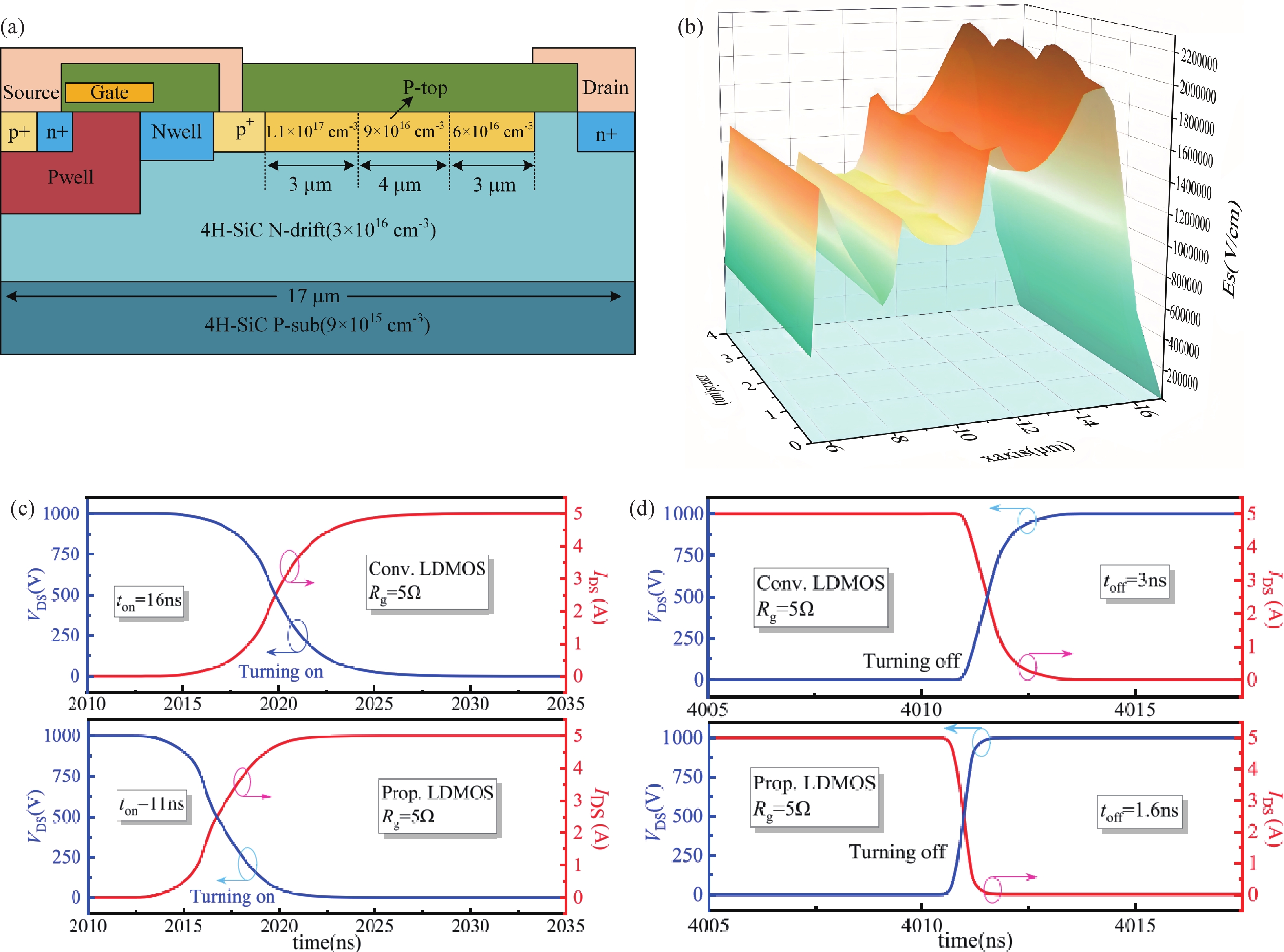

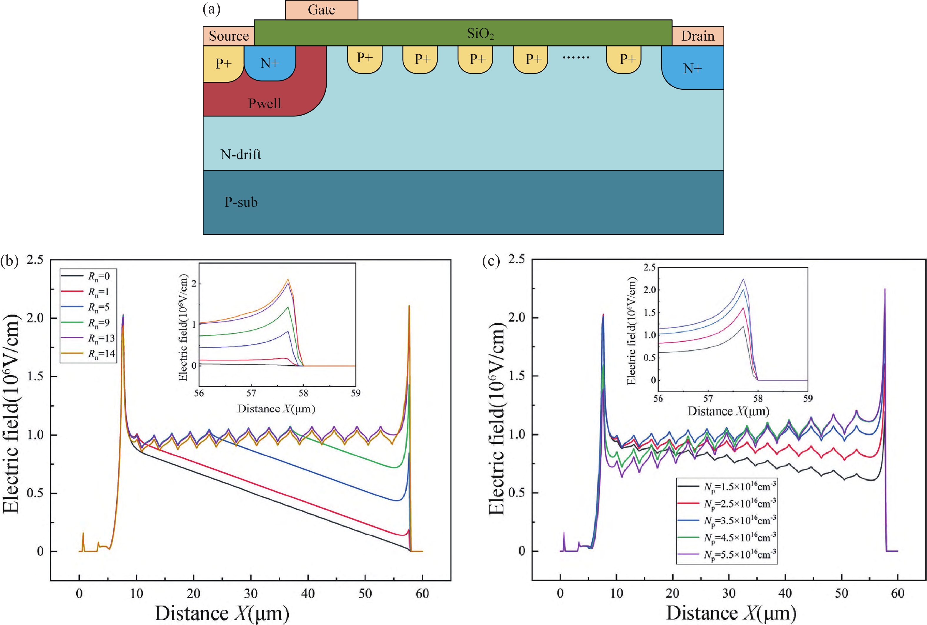
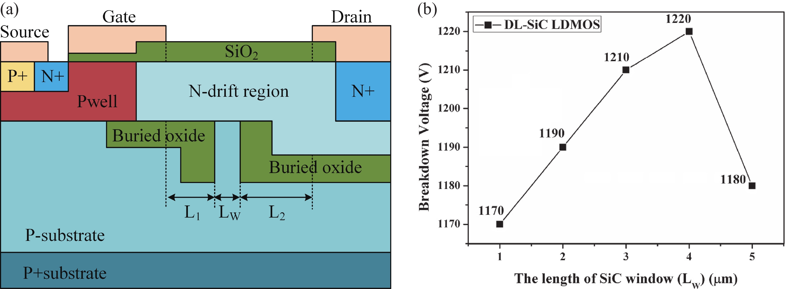
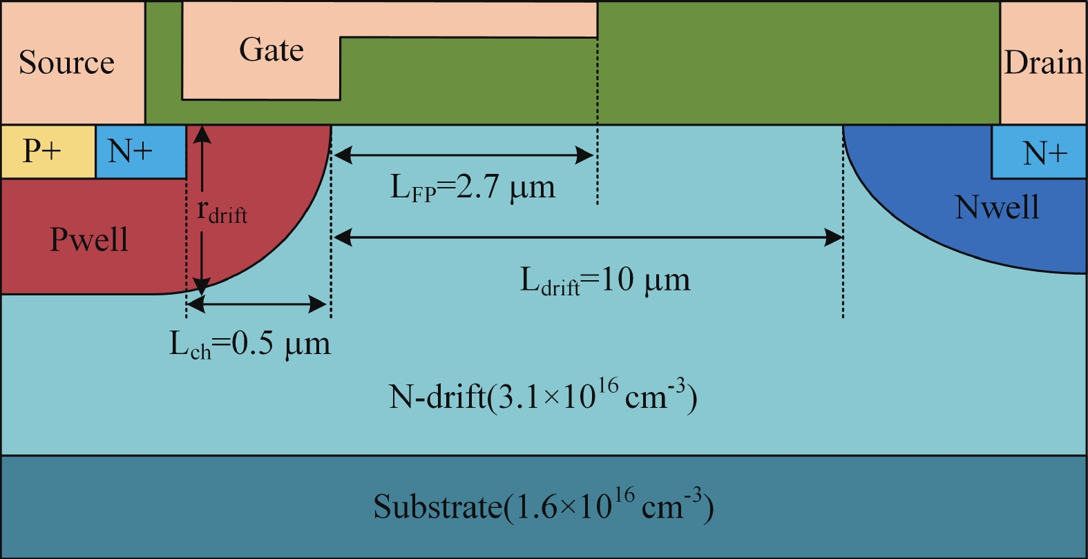

Table 1. Comparison of properties for SiC and other semiconductors.
| Parameters | Si | GaN | 3C-SiC | 6H-SiC | 4H-SiC |
| Band gap Eg (eV) | 1.1 | 3.4 | 2.3 | 3.03 | 3.25 |
| Electron mobility μ (cm2/(V·s)) | 1400 | 900 | 1000 | 450 | 1000 |
| Relative dielectric constant ε | 11.8 | 9.0 | 9.7 | 9.7 | 9.7 |
| Thermal conductivity λ (W/(cm·k)) | 1.5 | 2.0 | 4.9 | 4.9 | 4.9 |
| Breakdown electric field Eb (MV/cm) | 0.3 | 3.3 | 4 | 5 | 2.5 |
 DownLoad: CSV
Table 2. Comparison of electric performances for SiC LDMOS power devices.
| Structures | Channel mobility (cm2/(V∙s)) |
Ron,sp (mΩ∙cm2) |
BV (V) |
BFOM (MW/cm2) | Current | Refs | Experiment (E) or simulation (S) |
| The first 4H-SiC LDMOS | 5 | 200 | 2600 | 33 | 0.25 mA (Vgs = 25 V) |
[9] | E |
| 4H-SiC lateral MOSFET with NO annealing |
25 | 170 | 930 | 5.09 | 6.5 mA (Vgs = 24 V) |
[20] | E |
| 6H-SiC lateral MOSFET with two RESURF zones |
30 | 160 | 1300 | 10.56 | 25 mA (Vgs = 30 V) |
[48] | E |
| 4H-SiC lateral MOSFET with two-zone RESURF | 17 | 66 | 1380 | 28.85 | 20 mA | [52] | E |
| 4H-SiC LDMOS on HPSI substrate | 35 | 600 | 3520 | 20.6 | / | [61] | E |
| 4H-SiC LDMOS with trench-gate structure | / | 97 | 440 | 1.99 | 1.2 mA/μm (Vgs = 10 V) |
[35] | S |
| 4H-SiC LDMOS with gate field plates | / | 59.75 | 934 | 14.6 | 19 mA/mm (Vgs = 25 V) |
[60] | E |
| 4H-SiC LDMOS with current path layer | 21.7 | 89.8 | 1093 | 13.3 | 22 mA/mm (Vgs = 25 V) |
[71] | E |
| SiC LDMOS with two L-shaped oxide layers | / | 18.79 | 1220 | 79.2 | / | [67] | S |
| 4H-SiC lateral MOSFET with a P-top layer |
17 | 13.7 | 600 | 97.3 | 10 A (Vgs = 25 V) |
[54] | E |
| 4H-SiC LDMOS with double-trench gate | / | 3.5 | 1460 | 609 | 1 mA (Vgs = 20 V) |
[36] | S |
| 4H-SiC lateral MOSFET with dual source trenches | 50 | 3.9 | 1540 | 608.1 | / | [37] | S |
| SiC lateral MOSFET with VLD P-top layer |
31 | 3.57 | 1500 | 630.2 | 0.8 A/mm (Vgs = 20 V) |
[58] | S |
| SiC lateral MOSFETS with SD P-top layer |
/ | 4.04 | 1934 | 925.8 | / | [59] | S |
DownLoad: CSV
| [1] |
Li J Y, Zhao Y M, Liu X F, et al. Uniformity investigation in 3C-SiC epitaxial layers grown on Si substrates by horizontal hot-wall CVD. J Semicond, 2006, 28(1), 1
|
| [2] |
Yan G G, Sun G S, Wu H L, et al. Multi-wafer 3C-SiC thin films grown on Si (100) in a vertical HWLPCVD reactor. J Semicond, 2011, 32(6), 063001 doi: 10.1088/1674-4926/32/6/063001
|
| [3] |
Liu M, Yang Y, Mao Q, et al. Influence of radio frequency magnetron sputtering parameters on the structure and performance of SiC films. Ceram Int, 2021, 47(17), 24098 doi: 10.1016/j.ceramint.2021.05.120
|
| [4] |
Pelt J S, Ramsey M E, Durbin S M. Characterization of crystalline SiC films grown by pulsed laser deposition. Thin Solid Films, 2000, 371(1-2), 72 doi: 10.1016/S0040-6090(00)00991-3
|
| [5] |
Nishino S, Powell J A, Will H A. Production of large-area single-crystal wafers of cubic SiC for semiconductor devices. Appl Phys Lett, 1983, 42(5), 460 doi: 10.1063/1.93970
|
| [6] |
Powell J A, Matus L G, Kuczmarski M A. Growth and characterization of cubic SiC single-crystal films on Si. J Electrochem Soc, 1987, 134(6), 1558 doi: 10.1149/1.2100708
|
| [7] |
Ning P Q, Yuan T S, Kang Y H, et al. Review of Si IGBT and SiC MOSFET based on hybrid switch. Chin J Electr Eng, 2019, 5(3), 20 doi: 10.23919/CJEE.2019.000017
|
| [8] |
Kaur R, Gupta P, Singh J. A review on power MOSFET device structures. Int J Res Appl Sci Eng Technol, 2017, 5(X), 208 doi: 10.22214/IJRASET.2017.10034
|
| [9] |
Spitz J, Melloch M R, Cooper J A, et al. 2.6 kV 4H-SiC lateral DMOSFETs. IEEE Electron Device Lett, 1998, 19(4), 100 doi: 10.1109/55.663527
|
| [10] |
Chen G, Bai S, Zhang T, et al. 4H-SiC MESFET device process. J Semicond, 2007, 28(S1), 565
|
| [11] |
Kukushkin S A, Osipov A V, Feoktistov N A. Synthesis of epitaxial silicon carbide films through the substitution of atoms in the silicon crystal lattice: A review. Phys Solid State, 2014, 56(8), 1507 doi: 10.1134/S1063783414080137
|
| [12] |
Kong M F, Duan Y M, Zhang B K, et al. A novel 4H-SiC accumulation mode MOSFET with ultra-low specific on-resistance and improved reverse recovery capability. IET Power Electron, 2023, 16(14), 2369 doi: 10.1049/pel2.12556
|
| [13] |
Luo X R, Liao T, Wei J, et al. A novel 4H-SiC trench MOSFET with double shielding structures and ultralow gate-drain charge. J Semicond, 2019, 40(5), 052803 doi: 10.1088/1674-4926/40/5/052803
|
| [14] |
Kimoto T. Updated trade-off relationship between specific on-resistance and breakdown voltage in 4H-SiC{0001} unipolar devices. Jpn J Appl Phys, 2019, 58(1), 018002 doi: 10.7567/1347-4065/aae896
|
| [15] |
Bhatnagar M, Baliga B J. Comparison of 6H-SiC, 3C-SiC, and Si for power devices. IEEE Trans Electron Devices, 1993, 40(3), 645 doi: 10.1109/16.199372
|
| [16] |
Weiße J, Matthus C, Schlichting H, et al. RESURF n-LDMOS transistor for advanced integrated circuits in 4H-SiC. IEEE Trans Electron Devices, 2020, 67(8), 3278 doi: 10.1109/TED.2020.3002730
|
| [17] |
Fukuda K, Cho W J, Arai K, et al. Effect of oxidation method and post-oxidation annealing on interface properties of metal–oxide–semiconductor structures formed on n-type 4H-SiC C(0001̄) face. Appl Phys Lett, 2000, 77(6), 866 doi: 10.1063/1.1306649
|
| [18] |
Fukuda K, Senzaki J, Kojima K, et al. High inversion channel mobility of MOSFET fabricated on 4H-SiC C(000-1) face using H2 post-oxidation annealing. Mater Sci Forum, 2003, 567 doi: 10.4028/www.scientific.net/MSF.433-436.567
|
| [19] |
Okamoto M, Suzuki S, Kato M, et al. Lateral RESURF MOSFET fabricated on 4H-SiC ( $ 000\bar{\text{1}} $) C-face. IEEE Electron Device Lett, 2004, 25(6), 405 doi: 10.1109/LED.2004.828970
|
| [20] |
Wang W, Banerjee S, Chow T P, et al. 930-V 170-mΩ·cm2 lateral two-zone RESURF MOSFETs in 4H-SiC with NO annealing. IEEE Electron Device Lett, 2004, 25(4), 185 doi: 10.1109/LED.2004.825196
|
| [21] |
Chen X D, Dhar S, Isaacs-Smith T, et al. Electron capture and emission properties of interface states in thermally oxidized and NO-annealed SiO2/4H-SiC. J Appl Phys, 2008, 103(3), 033701 doi: 10.1063/1.2837028
|
| [22] |
Chung G Y, Tin C C, Williams J R, et al. Effect of nitric oxide annealing on the interface trap densities near the band edges in the 4H polytype of silicon carbide. Appl Phys Lett, 2000, 76(13), 1713 doi: 10.1063/1.126167
|
| [23] |
Biggerstaff T L, Reynolds C L Jr, Zheleva T, et al. Relationship between 4H-SiC∕SiO2 transition layer thickness and mobility. Appl Phys Lett, 2009, 95(3), 032108 doi: 10.1063/1.3144272
|
| [24] |
Kimoto T, Kanzaki Y, Noborio M, et al. Interface properties of metal–oxide–semiconductor structures on 4H-SiC{0001} and (1120) formed by N2O oxidation. Jpn J Appl Phys, 2005, 44(3R), 1213 doi: 10.1143/JJAP.44.1213
|
| [25] |
Kimoto T, Kosugi H, Suda J, et al. Design and fabrication of RESURF MOSFETs on 4H-SiC(0001), (112~0), and 6H-SiC(0001). IEEE Trans Electron Devices, 2005, 52(1), 112 doi: 10.1109/TED.2004.841358
|
| [26] |
Fujihira K, Tarui Y, Imaizumi M, et al. Characteristics of 4H–SiC MOS interface annealed in N2O. Solid State Electron, 2005, 49(6), 896 doi: 10.1016/j.sse.2004.10.016
|
| [27] |
Yun N, Sung W. Design and fabrication approaches of 400–600 V 4H-SiC lateral MOSFETs for emerging power ICs application. IEEE Trans Electron Devices, 2020, 67(11), 5005 doi: 10.1109/TED.2020.3027652
|
| [28] |
Fiorenza P, Bongiorno C, Giannazzo F, et al. Interfacial electrical and chemical properties of deposited SiO2 layers in lateral implanted 4H-SiC MOSFETs subjected to different nitridations. Appl Surf Sci, 2021, 557, 149752 doi: 10.1016/j.apsusc.2021.149752
|
| [29] |
Singh R, Capell D C, Das M K, et al. Development of high-current 4H-SiC ACCUFET. IEEE Trans Electron Devices, 2003, 50(2), 471 doi: 10.1109/TED.2002.808511
|
| [30] |
Zhu Z Y, Xu H Y, Liu L, et al. Investigation on surge current capability of 4H-SiC trench-gate MOSFETs in third quadrant under various VGS biases. IEEE J Emerg Sel Top Power Electron, 2021, 9(5), 6361 doi: 10.1109/JESTPE.2020.3028094
|
| [31] |
Williams R K, Darwish M N, Blanchard R A, et al. The trench power MOSFET: Part I—History, technology, and prospects. IEEE Trans Electron Devices, 2017, 64(3), 674 doi: 10.1109/TED.2017.2653239
|
| [32] |
Zareiee M. A novel dual trench gate power device by effective drift region structure. Superlattices Microstruct, 2019, 125, 8 doi: 10.1016/j.spmi.2018.10.019
|
| [33] |
Shen P, Wang Y, Li X J, et al. Improved 4H-SiC UMOSFET with super-junction shield region. Chin Phys B, 2021, 30(5), 058502 doi: 10.1088/1674-1056/abd740
|
| [34] |
Shen P, Wang Y, Cao F. A 4H-SiC trench MOSFET structure with wrap N-type pillar for low oxide field and enhanced switching performance. Chin Phys B, 2022, 31(7), 078501 doi: 10.1088/1674-1056/ac4e08
|
| [35] |
Singh Y, Dwivedi D. Simulation study of dual-gate trench LDMOSFET on 4H-SiC. 2015 Second International Conference on Advances in Computing and Communication Engineering, 2015, 174 doi: 10.1109/ICACCE.2015.5044
|
| [36] |
Kong M F, Hu Z W, Gao J C, et al. A 1200-V-class ultra-low specific on-resistance SiC lateral MOSFET with double trench gate and VLD technique. IEEE J Electron Devices Soc, 2022, 10, 83 doi: 10.1109/JEDS.2021.3136341
|
| [37] |
Wang H Y, Wang B Z, Kong L X, et al. 4H-SiC trench gate lateral MOSFET with dual source trenches for improved performance and reliability. IEEE Trans Device Mater Reliab, 2023, 23(1), 2 doi: 10.1109/TDMR.2022.3222909
|
| [38] |
Zhuang X, Qiao M, Zhang B, et al. Analysis of the breakdown mechanism for an ultra high voltage high-side thin layer silicon-on-insulator p-channel lateral double-diffused metal-oxide semiconductor. Chin Phys B, 2012, 21(3), 037305 doi: 10.1088/1674-1056/21/3/037305
|
| [39] |
Yang Y T, Duan B X. The application of the electric field modulation and charge shielding effects to the high-voltage Si LDMOS. IETE Tech Rev, 2012, 29(4), 276 doi: 10.4103/0256-4602.101307
|
| [40] |
Mehrad M, Orouji A A, Taheri M. A new technique in LDMOS transistors to improve the breakdown voltage and the lattice temperature. Mater Sci Semicond Process, 2015, 34, 276 doi: 10.1016/j.mssp.2015.02.057
|
| [41] |
Xu J, He N L, Liang H L, et al. Terminal-optimized 700-V LDMOS with improved breakdown voltage and ESD robustness. Chin Phys B, 2021, 30(6), 067303 doi: 10.1088/1674-1056/abdda7
|
| [42] |
Li Q, Li H O, Huang P J, et al. Improving breakdown voltage performance of SOI power device with folded drift region. Chin Phys B, 2016, 25(7), 077201 doi: 10.1088/1674-1056/25/7/077201
|
| [43] |
Chen W Z, Huang Y X, Huang Y, et al. A super-junction SOI-LDMOS with low resistance electron channel. Chin Phys B, 2021, 30(5), 057303 doi: 10.1088/1674-1056/abe374
|
| [44] |
Appels J A, Vaes H M J. High voltage thin layer devices (RESURF devices). 1979 International Electron Devices Meeting, 1979, 238 doi: 10.1109/IEDM.1979.18958946
|
| [45] |
Qiao M, Li Y, Yuan Z, et al. A novel ultralow RON, sp triple RESURF LDMOS with sandwich n-p-n layer. IEEE Trans Electron Devices, 2020, 67(12), 5605 doi: 10.1109/TED.2020.3030872
|
| [46] |
Houadef A, Djezzar B. Process and performance optimization of triple-RESURF LDMOS with trenched-gate. Int J RF Microw Comput Aided Eng, 2021, 31(10), e22755 doi: 10.1002/mmce.2275549
|
| [47] |
Banerjee S, Chatty K, Chow T P, et al. Improved high-voltage lateral RESURF MOSFETs in 4H-SiC. IEEE Electron Device Lett, 2001, 22(5), 209 doi: 10.1109/55.919231
|
| [48] |
Banerjee S, Chow T P, Gutmann R J. 1300-V 6H-SiC lateral MOSFETs with two RESURF zones. IEEE Electron Device Lett, 2002, 23(10), 624 doi: 10.1109/LED.2002.803768
|
| [49] |
Noborio M, Jun S D, Kimoto T. 1.5 kV lateral double RESURF MOSFETs on 4H-SiC (000-1)C face. Mater Sci Forum, 2009, 757 doi: 10.4028/www.scientific.net/MSF.615-617.757
|
| [50] |
Noborio M, Jun S D, Kimoto T. Improved performance of 4H-SiC double reduced surface field metal–oxide–semiconductor field-effect transistors by increasing RESURF doses. Appl Phys Express, 2008, 1(10), 101403 doi: 10.1143/APEX.1.101403
|
| [51] |
Noborio M, Jun S D, Kimoto T. Lateral 4H-SiC MOSFETs with low on-resistance by using two-zone double RESURF structure. Mater Sci Forum, 2007, 815 doi: 10.4028/www.scientific.net/MSF.556-557.81553
|
| [52] |
Noborio M, Jun S D, Kimoto T. 4H–SiC lateral double RESURF MOSFETs with low on resistance. IEEE Trans Electron Devices, 2007, 54(5), 1216 doi: 10.1109/TED.2007.894249
|
| [53] |
Noborio M, Suda J, Kimoto T. Dose designing and fabrication of 4H-SiC double RESURF MOSFETs. 2006 IEEE International Symposium on Power Semiconductor Devices and IC’s, 2006, 1 doi: 10.1109/ISPSD.2006.1666124
|
| [54] |
Yun N, Lynch J, Sung W. Demonstration and analysis of a 600 V, 10 A, 4H-SiC lateral single RESURF MOSFET for power ICs applications. Appl Phys Lett, 2019, 114(19), 192104 doi: 10.1063/1.5094407
|
| [55] |
Liu L, Wang J, Wang Z S, et al. Electrical characterization and analysis of 4H-SiC lateral MOSFET (LMOS) for high-voltage power integrated circuits. 2023 35th International Symposium on Power Semiconductor Devices and ICs, 2023, 366 doi: 10.1109/ISPSD57135.2023.10147418
|
| [56] |
Agarwal A K, Seshadri S, Rowland L B. Temperature dependence of Fowler-Nordheim current in 6H-and 4H-SiC MOS capacitors. IEEE Electron Device Lett, 1997, 18(12), 592 doi: 10.1109/55.644081
|
| [57] |
Liu L, Guo Q, Wang J, et al. Design and experimental demonstration of 4H-SiC lateral high-voltage MOSFETs with double-RESURFs technology for power ICs. IEEE Trans Electron Devices, 2024, 71(3), 1572 doi: 10.1109/TED.2024.3354874
|
| [58] |
Kong M F, Duan Y M, Gao J C, et al. A novel optimum variation lateral doping SiC lateral double-diffused metal oxide semiconductor with improved performance. Semicond Sci Technol, 2022, 37(10), 105022 doi: 10.1088/1361-6641/ac88f0
|
| [59] |
Yu H, Wang J, Liu L, et al. A novel SiC LDMOS with electric field optimization by step doping technology. 2020 17th China International Forum on Solid State Lighting & 2020 International Forum on Wide Bandgap Semiconductors China (SSLChina: IFWS), 2020, 23
|
| [60] |
Seok O, Kim H W, Moon J H, et al. High-voltage lateral double-implanted MOSFETs implemented on high-purity semi-insulating 4H-SiC substrates with gate field plates. Jpn J Appl Phys, 2018, 57(6S1), 06HC08 doi: 10.7567/JJAP.57.06HC08
|
| [61] |
Lee W S, Lin C W, Yang M H, et al. Demonstration of 3500-V 4H-SiC lateral MOSFETs. IEEE Electron Device Lett, 2011, 32(3), 360 doi: 10.1109/LED.2010.2101041
|
| [62] |
Sporea R A, Trainor M J, Young N D, et al. Field plate optimization in low-power high-gain source-gated transistors. IEEE Trans Electron Devices, 2012, 59(8), 2180 doi: 10.1109/TED.2012.2198823
|
| [63] |
Shimbori A, Huang A Q. A novel 600V lateral RESURF 4H-SiC MESFET with sloped field plate for high power and high frequency applications. 2020 IEEE Workshop on Wide Bandgap Power Devices and Applications in Asia (WiPDA Asia), 2020, 1 doi: 10.1109/WiPDAAsia49671.2020.9360295
|
| [64] |
Peng H Y, Wang Z X, Gao J H, et al. Breakdown characteristics of SiC LDMOS with multi-field limiting ring structure. Electron Compon Mater, 2023, 42(1), 50 (in Chinese) doi: 10.14106/j.cnki.1001-2028.2023.1374
|
| [65] |
Hirao T, Onose H, Kan Y S, et al. Edge termination with enhanced field-limiting rings insensitive to surface charge for high-voltage SiC power devices. IEEE Trans Electron Devices, 2020, 67(7), 2850 doi: 10.1109/TED.2020.2992577
|
| [66] |
Li Q, Zhu J L, Wang W D, et al. A novel thin drift region device with field limiting rings in substrate. Chin Phys B, 2011, 20(11), 117202 doi: 10.1088/1674-1056/20/11/117202
|
| [67] |
Bao M T, Wang Y. Improving breakdown voltage and self-heating effect for SiC LDMOS with double L-shaped buried oxide layers. Superlattices Microstruct, 2017, 102, 147 doi: 10.1016/j.spmi.2016.12.038
|
| [68] |
Wang Y, Bao M T, Wang Y F, et al. An improved SOI LDMOS with buried field plate. Superlattices Microstruct, 2017, 111, 340 doi: 10.1016/j.spmi.2017.06.049
|
| [69] |
Dong Z M, Duan B X, Fu C, et al. Novel LDMOS optimizing lateral and vertical electric field to improve breakdown voltage by multi-ring technology. IEEE Electron Device Lett, 2018, 39(9), 1358 doi: 10.1109/LED.2018.2854417
|
| [70] |
Zhang C W, Yao Z B, Guo H J, et al. A novel LDMOS with circular drift region for uniform electric field distribution. Micro Nanostruct, 2023, 175, 207511 doi: 10.1016/j.micrna.2023.207511
|
| [71] |
Kim H W, Seok O, Moon J H, et al. Fabrication of 4H-SiC lateral double implanted MOSFET on an on-axis semi-insulating substrate without using epi-layer. Jpn J Appl Phys, 2017, 56(12), 120305 doi: 10.7567/JJAP.56.120305
|


Article views: 5856 Times PDF downloads: 979 Times Cited by: 0 Times
Received: 30 January 2024 Revised: 29 March 2024 Online: Accepted Manuscript: 29 April 2024Uncorrected proof: 06 May 2024Published: 15 August 2024
| Citation: |
Ziwei Hu, Jiafei Yao, Ang Li, Qi Sun, Man Li, Kemeng Yang, Jun Zhang, Jing Chen, Maolin Zhang, Yufeng Guo. Review of the SiC LDMOS power device[J]. Journal of Semiconductors, 2024, 45(8): 081501. doi: 10.1088/1674-4926/24010029
****
Z W Hu, J F Yao, A Li, Q Sun, M Li, K M Yang, J Zhang, J Chen, M L Zhang, and Y F Guo, Review of the SiC LDMOS power device[J]. J. Semicond., 2024, 45(8), 081501 doi: 10.1088/1674-4926/24010029

|
 Ziwei Hu received his bachelor's degree from Nanjing University of Posts and Telecommunications in 2023. Now he is a Ph. D. candidate student at Nanjing University of Posts and Telecommunications under the supervision of Prof. Yufeng Guo. He focuses on the research of silicon carbide power devices
 Jiafei Yao received his Ph.D. degree in microelectronics and solid-state electronics from Nanjing University of Posts and Telecommunications. Currently, he is an associate professor with the School of Integrated Circuit Science and Engineering, Nanjing University of Posts and Telecommunications, Nanjing, China. His research focuses on the silicon power devices, silicon carbide power devices and power integrated circuits
 Yufeng Guo received the Ph.D. degree in microelectronics and solid-state electronics from the University of Electronic Science and Technology of China, Chengdu, China, in 2005. He is currently a Professor with the School of Integrated Circuit Science and Engineering, Nanjing University of Posts and Telecommunications, Nanjing, China. He has published more than 250 articles in refereed journals and conferences and holding over 60 Chinese patents. His current research interests include semiconductor power devices, microelectronics devices reliability, and RF and power integrated circuits and systems
| [1] |
Li J Y, Zhao Y M, Liu X F, et al. Uniformity investigation in 3C-SiC epitaxial layers grown on Si substrates by horizontal hot-wall CVD. J Semicond, 2006, 28(1), 1
|
| [2] |
Yan G G, Sun G S, Wu H L, et al. Multi-wafer 3C-SiC thin films grown on Si (100) in a vertical HWLPCVD reactor. J Semicond, 2011, 32(6), 063001 doi: 10.1088/1674-4926/32/6/063001
|
| [3] |
Liu M, Yang Y, Mao Q, et al. Influence of radio frequency magnetron sputtering parameters on the structure and performance of SiC films. Ceram Int, 2021, 47(17), 24098 doi: 10.1016/j.ceramint.2021.05.120
|
| [4] |
Pelt J S, Ramsey M E, Durbin S M. Characterization of crystalline SiC films grown by pulsed laser deposition. Thin Solid Films, 2000, 371(1-2), 72 doi: 10.1016/S0040-6090(00)00991-3
|
| [5] |
Nishino S, Powell J A, Will H A. Production of large-area single-crystal wafers of cubic SiC for semiconductor devices. Appl Phys Lett, 1983, 42(5), 460 doi: 10.1063/1.93970
|
| [6] |
Powell J A, Matus L G, Kuczmarski M A. Growth and characterization of cubic SiC single-crystal films on Si. J Electrochem Soc, 1987, 134(6), 1558 doi: 10.1149/1.2100708
|
| [7] |
Ning P Q, Yuan T S, Kang Y H, et al. Review of Si IGBT and SiC MOSFET based on hybrid switch. Chin J Electr Eng, 2019, 5(3), 20 doi: 10.23919/CJEE.2019.000017
|
| [8] |
Kaur R, Gupta P, Singh J. A review on power MOSFET device structures. Int J Res Appl Sci Eng Technol, 2017, 5(X), 208 doi: 10.22214/IJRASET.2017.10034
|
| [9] |
Spitz J, Melloch M R, Cooper J A, et al. 2.6 kV 4H-SiC lateral DMOSFETs. IEEE Electron Device Lett, 1998, 19(4), 100 doi: 10.1109/55.663527
|
| [10] |
Chen G, Bai S, Zhang T, et al. 4H-SiC MESFET device process. J Semicond, 2007, 28(S1), 565
|
| [11] |
Kukushkin S A, Osipov A V, Feoktistov N A. Synthesis of epitaxial silicon carbide films through the substitution of atoms in the silicon crystal lattice: A review. Phys Solid State, 2014, 56(8), 1507 doi: 10.1134/S1063783414080137
|
| [12] |
Kong M F, Duan Y M, Zhang B K, et al. A novel 4H-SiC accumulation mode MOSFET with ultra-low specific on-resistance and improved reverse recovery capability. IET Power Electron, 2023, 16(14), 2369 doi: 10.1049/pel2.12556
|
| [13] |
Luo X R, Liao T, Wei J, et al. A novel 4H-SiC trench MOSFET with double shielding structures and ultralow gate-drain charge. J Semicond, 2019, 40(5), 052803 doi: 10.1088/1674-4926/40/5/052803
|
| [14] |
Kimoto T. Updated trade-off relationship between specific on-resistance and breakdown voltage in 4H-SiC{0001} unipolar devices. Jpn J Appl Phys, 2019, 58(1), 018002 doi: 10.7567/1347-4065/aae896
|
| [15] |
Bhatnagar M, Baliga B J. Comparison of 6H-SiC, 3C-SiC, and Si for power devices. IEEE Trans Electron Devices, 1993, 40(3), 645 doi: 10.1109/16.199372
|
| [16] |
Weiße J, Matthus C, Schlichting H, et al. RESURF n-LDMOS transistor for advanced integrated circuits in 4H-SiC. IEEE Trans Electron Devices, 2020, 67(8), 3278 doi: 10.1109/TED.2020.3002730
|
| [17] |
Fukuda K, Cho W J, Arai K, et al. Effect of oxidation method and post-oxidation annealing on interface properties of metal–oxide–semiconductor structures formed on n-type 4H-SiC C(0001̄) face. Appl Phys Lett, 2000, 77(6), 866 doi: 10.1063/1.1306649
|
| [18] |
Fukuda K, Senzaki J, Kojima K, et al. High inversion channel mobility of MOSFET fabricated on 4H-SiC C(000-1) face using H2 post-oxidation annealing. Mater Sci Forum, 2003, 567 doi: 10.4028/www.scientific.net/MSF.433-436.567
|
| [19] |
Okamoto M, Suzuki S, Kato M, et al. Lateral RESURF MOSFET fabricated on 4H-SiC ( $ 000\bar{\text{1}} $) C-face. IEEE Electron Device Lett, 2004, 25(6), 405 doi: 10.1109/LED.2004.828970
|
| [20] |
Wang W, Banerjee S, Chow T P, et al. 930-V 170-mΩ·cm2 lateral two-zone RESURF MOSFETs in 4H-SiC with NO annealing. IEEE Electron Device Lett, 2004, 25(4), 185 doi: 10.1109/LED.2004.825196
|
| [21] |
Chen X D, Dhar S, Isaacs-Smith T, et al. Electron capture and emission properties of interface states in thermally oxidized and NO-annealed SiO2/4H-SiC. J Appl Phys, 2008, 103(3), 033701 doi: 10.1063/1.2837028
|
| [22] |
Chung G Y, Tin C C, Williams J R, et al. Effect of nitric oxide annealing on the interface trap densities near the band edges in the 4H polytype of silicon carbide. Appl Phys Lett, 2000, 76(13), 1713 doi: 10.1063/1.126167
|
| [23] |
Biggerstaff T L, Reynolds C L Jr, Zheleva T, et al. Relationship between 4H-SiC∕SiO2 transition layer thickness and mobility. Appl Phys Lett, 2009, 95(3), 032108 doi: 10.1063/1.3144272
|
| [24] |
Kimoto T, Kanzaki Y, Noborio M, et al. Interface properties of metal–oxide–semiconductor structures on 4H-SiC{0001} and (1120) formed by N2O oxidation. Jpn J Appl Phys, 2005, 44(3R), 1213 doi: 10.1143/JJAP.44.1213
|
| [25] |
Kimoto T, Kosugi H, Suda J, et al. Design and fabrication of RESURF MOSFETs on 4H-SiC(0001), (112~0), and 6H-SiC(0001). IEEE Trans Electron Devices, 2005, 52(1), 112 doi: 10.1109/TED.2004.841358
|
| [26] |
Fujihira K, Tarui Y, Imaizumi M, et al. Characteristics of 4H–SiC MOS interface annealed in N2O. Solid State Electron, 2005, 49(6), 896 doi: 10.1016/j.sse.2004.10.016
|
| [27] |
Yun N, Sung W. Design and fabrication approaches of 400–600 V 4H-SiC lateral MOSFETs for emerging power ICs application. IEEE Trans Electron Devices, 2020, 67(11), 5005 doi: 10.1109/TED.2020.3027652
|
| [28] |
Fiorenza P, Bongiorno C, Giannazzo F, et al. Interfacial electrical and chemical properties of deposited SiO2 layers in lateral implanted 4H-SiC MOSFETs subjected to different nitridations. Appl Surf Sci, 2021, 557, 149752 doi: 10.1016/j.apsusc.2021.149752
|
| [29] |
Singh R, Capell D C, Das M K, et al. Development of high-current 4H-SiC ACCUFET. IEEE Trans Electron Devices, 2003, 50(2), 471 doi: 10.1109/TED.2002.808511
|
| [30] |
Zhu Z Y, Xu H Y, Liu L, et al. Investigation on surge current capability of 4H-SiC trench-gate MOSFETs in third quadrant under various VGS biases. IEEE J Emerg Sel Top Power Electron, 2021, 9(5), 6361 doi: 10.1109/JESTPE.2020.3028094
|
| [31] |
Williams R K, Darwish M N, Blanchard R A, et al. The trench power MOSFET: Part I—History, technology, and prospects. IEEE Trans Electron Devices, 2017, 64(3), 674 doi: 10.1109/TED.2017.2653239
|
| [32] |
Zareiee M. A novel dual trench gate power device by effective drift region structure. Superlattices Microstruct, 2019, 125, 8 doi: 10.1016/j.spmi.2018.10.019
|
| [33] |
Shen P, Wang Y, Li X J, et al. Improved 4H-SiC UMOSFET with super-junction shield region. Chin Phys B, 2021, 30(5), 058502 doi: 10.1088/1674-1056/abd740
|
| [34] |
Shen P, Wang Y, Cao F. A 4H-SiC trench MOSFET structure with wrap N-type pillar for low oxide field and enhanced switching performance. Chin Phys B, 2022, 31(7), 078501 doi: 10.1088/1674-1056/ac4e08
|
| [35] |
Singh Y, Dwivedi D. Simulation study of dual-gate trench LDMOSFET on 4H-SiC. 2015 Second International Conference on Advances in Computing and Communication Engineering, 2015, 174 doi: 10.1109/ICACCE.2015.5044
|
| [36] |
Kong M F, Hu Z W, Gao J C, et al. A 1200-V-class ultra-low specific on-resistance SiC lateral MOSFET with double trench gate and VLD technique. IEEE J Electron Devices Soc, 2022, 10, 83 doi: 10.1109/JEDS.2021.3136341
|
| [37] |
Wang H Y, Wang B Z, Kong L X, et al. 4H-SiC trench gate lateral MOSFET with dual source trenches for improved performance and reliability. IEEE Trans Device Mater Reliab, 2023, 23(1), 2 doi: 10.1109/TDMR.2022.3222909
|
| [38] |
Zhuang X, Qiao M, Zhang B, et al. Analysis of the breakdown mechanism for an ultra high voltage high-side thin layer silicon-on-insulator p-channel lateral double-diffused metal-oxide semiconductor. Chin Phys B, 2012, 21(3), 037305 doi: 10.1088/1674-1056/21/3/037305
|
| [39] |
Yang Y T, Duan B X. The application of the electric field modulation and charge shielding effects to the high-voltage Si LDMOS. IETE Tech Rev, 2012, 29(4), 276 doi: 10.4103/0256-4602.101307
|
| [40] |
Mehrad M, Orouji A A, Taheri M. A new technique in LDMOS transistors to improve the breakdown voltage and the lattice temperature. Mater Sci Semicond Process, 2015, 34, 276 doi: 10.1016/j.mssp.2015.02.057
|
| [41] |
Xu J, He N L, Liang H L, et al. Terminal-optimized 700-V LDMOS with improved breakdown voltage and ESD robustness. Chin Phys B, 2021, 30(6), 067303 doi: 10.1088/1674-1056/abdda7
|
| [42] |
Li Q, Li H O, Huang P J, et al. Improving breakdown voltage performance of SOI power device with folded drift region. Chin Phys B, 2016, 25(7), 077201 doi: 10.1088/1674-1056/25/7/077201
|
| [43] |
Chen W Z, Huang Y X, Huang Y, et al. A super-junction SOI-LDMOS with low resistance electron channel. Chin Phys B, 2021, 30(5), 057303 doi: 10.1088/1674-1056/abe374
|
| [44] |
Appels J A, Vaes H M J. High voltage thin layer devices (RESURF devices). 1979 International Electron Devices Meeting, 1979, 238 doi: 10.1109/IEDM.1979.18958946
|
| [45] |
Qiao M, Li Y, Yuan Z, et al. A novel ultralow RON, sp triple RESURF LDMOS with sandwich n-p-n layer. IEEE Trans Electron Devices, 2020, 67(12), 5605 doi: 10.1109/TED.2020.3030872
|
| [46] |
Houadef A, Djezzar B. Process and performance optimization of triple-RESURF LDMOS with trenched-gate. Int J RF Microw Comput Aided Eng, 2021, 31(10), e22755 doi: 10.1002/mmce.2275549
|
| [47] |
Banerjee S, Chatty K, Chow T P, et al. Improved high-voltage lateral RESURF MOSFETs in 4H-SiC. IEEE Electron Device Lett, 2001, 22(5), 209 doi: 10.1109/55.919231
|
| [48] |
Banerjee S, Chow T P, Gutmann R J. 1300-V 6H-SiC lateral MOSFETs with two RESURF zones. IEEE Electron Device Lett, 2002, 23(10), 624 doi: 10.1109/LED.2002.803768
|
| [49] |
Noborio M, Jun S D, Kimoto T. 1.5 kV lateral double RESURF MOSFETs on 4H-SiC (000-1)C face. Mater Sci Forum, 2009, 757 doi: 10.4028/www.scientific.net/MSF.615-617.757
|
| [50] |
Noborio M, Jun S D, Kimoto T. Improved performance of 4H-SiC double reduced surface field metal–oxide–semiconductor field-effect transistors by increasing RESURF doses. Appl Phys Express, 2008, 1(10), 101403 doi: 10.1143/APEX.1.101403
|
| [51] |
Noborio M, Jun S D, Kimoto T. Lateral 4H-SiC MOSFETs with low on-resistance by using two-zone double RESURF structure. Mater Sci Forum, 2007, 815 doi: 10.4028/www.scientific.net/MSF.556-557.81553
|
| [52] |
Noborio M, Jun S D, Kimoto T. 4H–SiC lateral double RESURF MOSFETs with low on resistance. IEEE Trans Electron Devices, 2007, 54(5), 1216 doi: 10.1109/TED.2007.894249
|
| [53] |
Noborio M, Suda J, Kimoto T. Dose designing and fabrication of 4H-SiC double RESURF MOSFETs. 2006 IEEE International Symposium on Power Semiconductor Devices and IC’s, 2006, 1 doi: 10.1109/ISPSD.2006.1666124
|
| [54] |
Yun N, Lynch J, Sung W. Demonstration and analysis of a 600 V, 10 A, 4H-SiC lateral single RESURF MOSFET for power ICs applications. Appl Phys Lett, 2019, 114(19), 192104 doi: 10.1063/1.5094407
|
| [55] |
Liu L, Wang J, Wang Z S, et al. Electrical characterization and analysis of 4H-SiC lateral MOSFET (LMOS) for high-voltage power integrated circuits. 2023 35th International Symposium on Power Semiconductor Devices and ICs, 2023, 366 doi: 10.1109/ISPSD57135.2023.10147418
|
| [56] |
Agarwal A K, Seshadri S, Rowland L B. Temperature dependence of Fowler-Nordheim current in 6H-and 4H-SiC MOS capacitors. IEEE Electron Device Lett, 1997, 18(12), 592 doi: 10.1109/55.644081
|
| [57] |
Liu L, Guo Q, Wang J, et al. Design and experimental demonstration of 4H-SiC lateral high-voltage MOSFETs with double-RESURFs technology for power ICs. IEEE Trans Electron Devices, 2024, 71(3), 1572 doi: 10.1109/TED.2024.3354874
|
| [58] |
Kong M F, Duan Y M, Gao J C, et al. A novel optimum variation lateral doping SiC lateral double-diffused metal oxide semiconductor with improved performance. Semicond Sci Technol, 2022, 37(10), 105022 doi: 10.1088/1361-6641/ac88f0
|
| [59] |
Yu H, Wang J, Liu L, et al. A novel SiC LDMOS with electric field optimization by step doping technology. 2020 17th China International Forum on Solid State Lighting & 2020 International Forum on Wide Bandgap Semiconductors China (SSLChina: IFWS), 2020, 23
|
| [60] |
Seok O, Kim H W, Moon J H, et al. High-voltage lateral double-implanted MOSFETs implemented on high-purity semi-insulating 4H-SiC substrates with gate field plates. Jpn J Appl Phys, 2018, 57(6S1), 06HC08 doi: 10.7567/JJAP.57.06HC08
|
| [61] |
Lee W S, Lin C W, Yang M H, et al. Demonstration of 3500-V 4H-SiC lateral MOSFETs. IEEE Electron Device Lett, 2011, 32(3), 360 doi: 10.1109/LED.2010.2101041
|
| [62] |
Sporea R A, Trainor M J, Young N D, et al. Field plate optimization in low-power high-gain source-gated transistors. IEEE Trans Electron Devices, 2012, 59(8), 2180 doi: 10.1109/TED.2012.2198823
|
| [63] |
Shimbori A, Huang A Q. A novel 600V lateral RESURF 4H-SiC MESFET with sloped field plate for high power and high frequency applications. 2020 IEEE Workshop on Wide Bandgap Power Devices and Applications in Asia (WiPDA Asia), 2020, 1 doi: 10.1109/WiPDAAsia49671.2020.9360295
|
| [64] |
Peng H Y, Wang Z X, Gao J H, et al. Breakdown characteristics of SiC LDMOS with multi-field limiting ring structure. Electron Compon Mater, 2023, 42(1), 50 (in Chinese) doi: 10.14106/j.cnki.1001-2028.2023.1374
|
| [65] |
Hirao T, Onose H, Kan Y S, et al. Edge termination with enhanced field-limiting rings insensitive to surface charge for high-voltage SiC power devices. IEEE Trans Electron Devices, 2020, 67(7), 2850 doi: 10.1109/TED.2020.2992577
|
| [66] |
Li Q, Zhu J L, Wang W D, et al. A novel thin drift region device with field limiting rings in substrate. Chin Phys B, 2011, 20(11), 117202 doi: 10.1088/1674-1056/20/11/117202
|
| [67] |
Bao M T, Wang Y. Improving breakdown voltage and self-heating effect for SiC LDMOS with double L-shaped buried oxide layers. Superlattices Microstruct, 2017, 102, 147 doi: 10.1016/j.spmi.2016.12.038
|
| [68] |
Wang Y, Bao M T, Wang Y F, et al. An improved SOI LDMOS with buried field plate. Superlattices Microstruct, 2017, 111, 340 doi: 10.1016/j.spmi.2017.06.049
|
| [69] |
Dong Z M, Duan B X, Fu C, et al. Novel LDMOS optimizing lateral and vertical electric field to improve breakdown voltage by multi-ring technology. IEEE Electron Device Lett, 2018, 39(9), 1358 doi: 10.1109/LED.2018.2854417
|
| [70] |
Zhang C W, Yao Z B, Guo H J, et al. A novel LDMOS with circular drift region for uniform electric field distribution. Micro Nanostruct, 2023, 175, 207511 doi: 10.1016/j.micrna.2023.207511
|
| [71] |
Kim H W, Seok O, Moon J H, et al. Fabrication of 4H-SiC lateral double implanted MOSFET on an on-axis semi-insulating substrate without using epi-layer. Jpn J Appl Phys, 2017, 56(12), 120305 doi: 10.7567/JJAP.56.120305
|

 WeChat ID
Journal of Semiconductors © 2017 All Rights Reserved 京ICP备05085259号-2


