


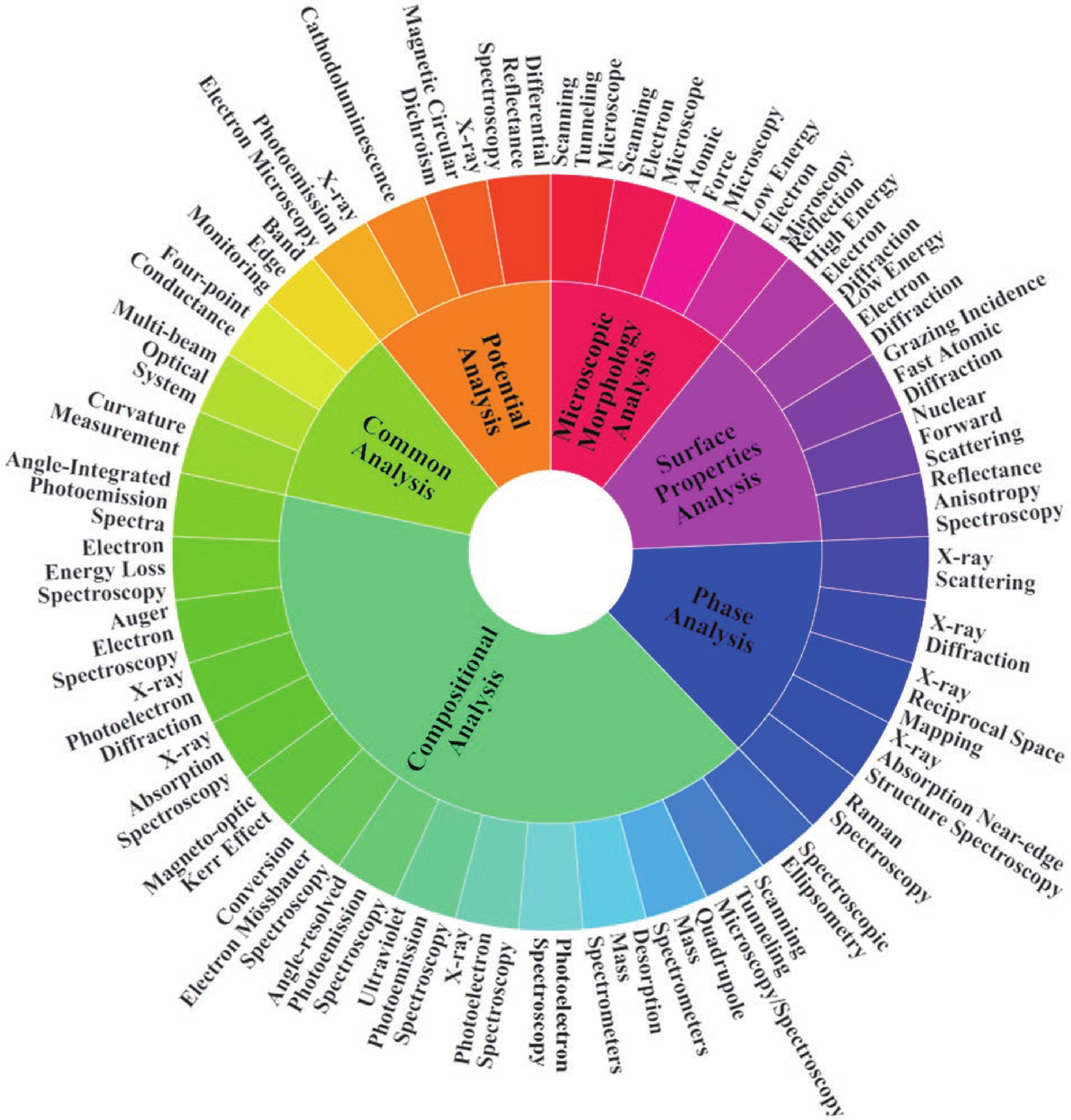
Fig. 1.
(Color online) In situ characterization techniques applied in MBE.
REVIEWS
Chao Shen1, 3, Wenkang Zhan1, 2, Manyang Li1, 2, Zhenyu Sun1, 2, , Jian Tang4, Zhaofeng Wu3, Chi Xu5, Bo Xu1, 2, Chao Zhao1, 2, and Zhanguo Wang1, 2
Corresponding author: Zhenyu Sun, zsun@semi.ac.cn; Chao Zhao, zhaochao@semi.ac.cn
Abstract: Ex situ characterization techniques in molecular beam epitaxy (MBE) have inherent limitations, such as being prone to sample contamination and unstable surfaces during sample transfer from the MBE chamber. In recent years, the need for improved accuracy and reliability in measurement has driven the increasing adoption of in situ characterization techniques. These techniques, such as reflection high-energy electron diffraction, scanning tunneling microscopy, and X-ray photoelectron spectroscopy, allow direct observation of film growth processes in real time without exposing the sample to air, hence offering insights into the growth mechanisms of epitaxial films with controlled properties. By combining multiple in situ characterization techniques with MBE, researchers can better understand film growth processes, realizing novel materials with customized properties and extensive applications. This review aims to overview the benefits and achievements of in situ characterization techniques in MBE and their applications for material science research. In addition, through further analysis of these techniques regarding their challenges and potential solutions, particularly highlighting the assistance of machine learning to correlate in situ characterization with other material information, we hope to provide a guideline for future efforts in the development of novel monitoring and control schemes for MBE growth processes with improved material properties.
Key words: epitaxial growth, thin film, in situ characterization, molecular beam epitaxy (MBE)
| [1] |
Nunn W, Truttmann T K, Jalan B. A review of molecular-beam epitaxy of wide bandgap complex oxide semiconductors. J Mater Res, 2021, 36, 4846 doi: 10.1557/s43578-021-00377-1
|
| [2] |
Zuo Z, Xu Z G, Zheng R J, et al. In-situ epitaxial growth of graphene/h-BN van der Waals heterostructures by molecular beam epitaxy. Sci Rep, 2015, 5, 14760 doi: 10.1038/srep14760
|
| [3] |
Zhao C, Ng T K, Wei N N, et al. Facile formation of high-quality InGaN/GaN quantum-disks-in-nanowires on bulk-metal substrates for high-power light-emitters. Nano Lett, 2016, 16, 1056 doi: 10.1021/acs.nanolett.5b04190
|
| [4] |
Priante D, Janjua B, Prabaswara A, et al. Highly uniform ultraviolet-a quantum-confined AlGaN nanowire LEDs on metal/silicon with a TaN interlayer. Opt Mater Express, 2017, 7, 4214 doi: 10.1364/OME.7.004214
|
| [5] |
Zhao C, Chen Y H, Xu B, et al. Evolution of InAs nanostructures grown by droplet epitaxy. Appl Phys Lett, 2007, 91, 033112 doi: 10.1063/1.2757151
|
| [6] |
Bollinger A T, Wu J, Božović I. Perspective: Rapid synthesis of complex oxides by combinatorial molecular beam epitaxy. APL Mater, 2016, 4, 053205 doi: 10.1063/1.4943989
|
| [7] |
Kim H S, Jeong J, Kwon G H, et al. Improvement of electrical performance using PtSe2/PtTe2 edge contact synthesized by molecular beam epitaxy. Appl Surf Sci, 2022, 585, 152507 doi: 10.1016/j.apsusc.2022.152507
|
| [8] |
Ma Y F, Zhang S C, Peng Z F, et al. Investigation on 1065 nm laser performance with Nd: GdLaNbO4 mixed crystal and molybdenum disulfide. Opt Laser Technol, 2019, 120, 105715 doi: 10.1016/j.optlastec.2019.105715
|
| [9] |
Bourree L E, Chasse D R, Stephan Thamban P L, et al. Comparison of the optical characteristics of GaAs photocathodes grown using MBE and MOCVDSPIE Proceedings. Low-Light-Level and Real-Time Imaging Systems, Components, and Applications. 2003, 11
|
| [10] |
Schubert F, Zybell S, Heitmann J, et al. Influence of the substrate grade on structural and optical properties of GaN/AlGaN superlattices. J Cryst Growth, 2015, 425, 145 doi: 10.1016/j.jcrysgro.2015.02.037
|
| [11] |
Opel M. Spintronic oxides grown by laser-MBE. J Phys D: Appl Phys, 2012, 45, 033001 doi: 10.1088/0022-3727/45/3/033001
|
| [12] |
Kosiel K. MBE—Technology for nanoelectronics. Vacuum, 2008, 82, 951 doi: 10.1016/j.vacuum.2008.01.033
|
| [13] |
Zekentes K, Papaioannou V, Pecz B, et al. Early stages of growth of β-SiC on Si by MBE. J Cryst Growth, 1995, 157, 392 doi: 10.1016/0022-0248(95)00330-4
|
| [14] |
Güsken N A, Rieger T, Zellekens P, et al. MBE growth of Al/InAs and Nb/InAs superconducting hybrid nanowire structures. Nanoscale, 2017, 9, 16735 doi: 10.1039/C7NR03982D
|
| [15] |
Iha H, Hirota Y, Yamauchi M, et al. Effect of arsenic cracking on in incorporation into MBE-grown InGaAs layer. Phys Status Solidi C, 2015, 12, 524 doi: 10.1002/pssc.201400286
|
| [16] |
Zhu K J, Bai Y H, Hong X Y, et al. Investigating and manipulating the molecular beam epitaxy growth kinetics of intrinsic magnetic topological insulator MnBi2Te4 with in situ angle-resolved photoemission spectroscopy. J Phys: Condens Matter, 2020, 32, 475002 doi: 10.1088/1361-648X/aba06d
|
| [17] |
Fan J Q, Wang S Z, Yu X Q, et al. Molecular beam epitaxy growth and surface structure of Sr1– x Nd x CuO2 cuprate films. Phys Rev B, 2020, 101, 180508 doi: 10.1103/PhysRevB.101.180508
|
| [18] |
Marin D V, Shvets V A, Azarov I A, et al. Ellipsometric thermometry in molecular beam epitaxy of mercury cadmium telluride. Infrared Phys Technol, 2021, 116, 103793 doi: 10.1016/j.infrared.2021.103793
|
| [19] |
Hilse M, Wang X Y, Killea P, et al. Spectroscopic ellipsometry as an in situ monitoring tool for Bi2Se3 films grown by molecular beam epitaxy. J Cryst Growth, 2021, 566/567, 126177 doi: 10.1016/j.jcrysgro.2021.126177
|
| [20] |
Botchkarev A, Salvador A, Sverdlov B, et al. Properties of GaN films grown under Ga and N rich conditions with plasma enhanced molecular beam epitaxy. J Appl Phys, 1995, 77, 4455 doi: 10.1063/1.359474
|
| [21] |
Peng H S, Li Q W, Chen T. Preface. Industrial applications of carbon nanotubes. Amsterdam: Elsevier, 2017
|
| [22] |
Karpov S Y, Talalaev R A, Makarov Y N, et al. Surface kinetics of GaN evaporation and growth by molecular-beam epitaxy. Surf Sci, 2000, 450, 191 doi: 10.1016/S0039-6028(00)00055-8
|
| [23] |
Mudiyanselage K, Katsiev K, Idriss H. Effects of experimental parameters on the growth of GaN nanowires on Ti-film/Si(1 0 0) and Ti-foil by molecular beam epitaxy. J Cryst Growth, 2020, 547, 125818 doi: 10.1016/j.jcrysgro.2020.125818
|
| [24] |
Jung Y W, Kim T J, Kim Y D, et al. Temperature dependence of the dielectric response of AlSb. AIP Conference Proceedings, 2011, 37 doi: 10.1063/1.3666246
|
| [25] |
Albert M, Golla C, Meier C. Optical in situ temperature management for high-quality ZnO molecular beam epitaxy. J Cryst Growth, 2021, 557, 126009 doi: 10.1016/j.jcrysgro.2020.126009
|
| [26] |
Fortin-Deschênes M, Waller O, Menteş T O, et al. Synthesis of antimonene on germanium. Nano Lett, 2017, 17, 4970 doi: 10.1021/acs.nanolett.7b02111
|
| [27] |
Zhang W, Enriquez H, Mayne A J, et al. First steps of blue phosphorene growth on Au(1 1 1). Mater Today, 2021, 39, 1153
|
| [28] |
Wang W, Zhou Q A, Dong Y A, et al. Critical thickness for strain relaxation of Ge1– x Sn x ( x ≤ 0.17) grown by molecular beam epitaxy on Ge(001). Appl Phys Lett, 2015, 106, 232106 doi: 10.1063/1.4922529
|
| [29] |
Kong Y, Bennett C J, Hyde C J. A review of non-destructive testing techniques for the in situ investigation of fretting fatigue cracks. Mater Des, 2020, 196, 109093 doi: 10.1016/j.matdes.2020.109093
|
| [30] |
Lin H J, Li H W, Shao H Y, et al. In situ measurement technologies on solid-state hydrogen storage materials: A review. Mater Today Energy, 2020, 17, 100463 doi: 10.1016/j.mtener.2020.100463
|
| [31] |
Zhernokletov D M, Dong H, Brennan B, et al. Investigation of arsenic and antimony capping layers, and half cycle reactions during atomic layer deposition of Al2O3 on GaSb(100). J Vac Sci Technol A, 2013, 31, 060602
|
| [32] |
Laukkanen P, Punkkinen M P J, Lång J J K, et al. Bismuth-containing c(4 × 4) surface structure of the GaAs(1 0 0) studied by synchrotron-radiation photoelectron spectroscopy and ab initio calculations. J Electron Spectrosc Relat Phenom, 2014, 193, 34 doi: 10.1016/j.elspec.2014.02.008
|
| [33] |
Zhang W, Wong P K J, Jiang S, et al. Integrating spin-based technologies with atomically controlled van der Waals interfaces. Mater Today, 2021, 51, 350 doi: 10.1016/j.mattod.2021.09.015
|
| [34] |
Lazarenko A A, Berezovskaya T N, Denisov D V, et al. Preparation of a silicon surface for subsequent growth of dilute nitride alloys by molecular-beam epitaxy. J Phys, 2017, 917, 32003 doi: 10.1088/1742-6596/917/3/032003
|
| [35] |
Kladko V, Kuchuk A, Lytvyn P, et al. Substrate effects on the strain relaxation in GaN/AlN short-period superlattices. Nanoscale Res Lett, 2012, 7, 289 doi: 10.1186/1556-276X-7-289
|
| [36] |
Zhang T, Levy N, Ha J, et al. Scanning tunneling microscopy of gate tunable topological insulator Bi2Se3 thin films. Phys Rev B, 2013, 87, 115410 doi: 10.1103/PhysRevB.87.115410
|
| [37] |
Bai A F, Hilse M, Patil P D, et al. Probing the growth quality of molecular beam epitaxy-grown Bi2Se3 films via in situ spectroscopic ellipsometry. J Cryst Growth, 2022, 591, 126714 doi: 10.1016/j.jcrysgro.2022.126714
|
| [38] |
Lin W Z, Foley A, Alam K, et al. Facility for low-temperature spin-polarized-scanning tunneling microscopy studies of magnetic/spintronic materials prepared in situ by nitride molecular beam epitaxy. Rev Sci Instrum, 2014, 85, 043702 doi: 10.1063/1.4870276
|
| [39] |
Huidobro J, Aramendia J, Arana G, et al. Reviewing in situ analytical techniques used to research Martian geochemistry: From the Viking project to the MMX future mission. Anal Chim Acta, 2022, 1197, 339499 doi: 10.1016/j.aca.2022.339499
|
| [40] |
Lin D M, Li K K, Zhou L M. Advanced in situ characterizations of nanocomposite electrodes for sodium-ion batteries-A short review. Compos Commun, 2021, 25, 100635 doi: 10.1016/j.coco.2021.100635
|
| [41] |
O'Hegarty R, Kinnane O, Lennon D, et al. In-situ U-value monitoring of highly insulated building envelopes: Review and experimental investigation. Energy Build, 2021, 252, 111447 doi: 10.1016/j.enbuild.2021.111447
|
| [42] |
Socha R P, Szczepanik-Ciba M, Powroźnik W, et al. Epitaxial α-Mn(001) films on MgO(001). Thin Solid Films, 2014, 556, 137 doi: 10.1016/j.tsf.2014.01.050
|
| [43] |
Yang R, Krzyzewski T, Jones T. The study of in situ scanning tunnelling microscope characterization on GaN thin film grown by plasma assisted molecular beam epitaxy. Appl Phys Lett, 2013, 102, 112104 doi: 10.1063/1.4795790
|
| [44] |
Kawasaki J K, Schultz B D, Lu H, et al. Surface-mediated tunable self-assembly of single crystal semimetallic ErSb/GaSb nanocomposite structures. Nano Lett, 2013, 13, 2895 doi: 10.1021/nl4012563
|
| [45] |
Hernández-Rodríguez I, García J M, Martín-Gago J A, et al. Graphene growth on Pt(111) and Au(111) using a MBE carbon solid-source. Diam Relat Mater, 2015, 57, 58 doi: 10.1016/j.diamond.2015.03.004
|
| [46] |
Haze M, Torii Y, Peters R, et al. In situ STM observation of nonmagnetic impurity effect in MBE-grown CeCoIn5 films. J Phys Soc Jpn, 2018, 87, 034702 doi: 10.7566/JPSJ.87.034702
|
| [47] |
Cai X Q, Xu Z L, Zhou H, et al. Epitaxial growth and band structure of antiferromagnetic Mott insulator CeOI. Phys Rev Materials, 2020, 4, 064003 doi: 10.1103/PhysRevMaterials.4.064003
|
| [48] |
Dávila M E, Xian L, Cahangirov S, et al. Germanene: A novel two-dimensional germanium allotrope akin to graphene and silicene. New J Phys, 2014, 16, 095002 doi: 10.1088/1367-2630/16/9/095002
|
| [49] |
Allongue P, Maroun F. Electrodeposited magnetic layers in the ultrathin limit. MRS Bull, 2010, 35, 761 doi: 10.1557/mrs2010.505
|
| [50] |
Wu Z B, Putzky D, Kundu A K, et al. Homogeneous superconducting gap in DyBa2Cu3O7– δ synthesized by oxide molecular beam epitaxy. Phys Rev Materials, 2020, 4, 124801 doi: 10.1103/PhysRevMaterials.4.124801
|
| [51] |
Song C L, Wang Y L, Jiang Y P, et al. Topological insulator Bi2Se3 thin films grown on double-layer graphene by molecular beam epitaxy. Appl Phys Lett, 2010, 97, 143118 doi: 10.1063/1.3494595
|
| [52] |
Toujyou T, Tsukamoto S. Temperature-dependent site control of InAs/GaAs (001) quantum dots using a scanning tunneling microscopy tip during growth. Nanoscale Res Lett, 2010, 5, 1930 doi: 10.1007/s11671-010-9802-z
|
| [53] |
Toujyou T, Tsukamoto S. in situ STM observation during InAs growth in nano holes at 300 °C. Surf Sci, 2011, 605, 1320 doi: 10.1016/j.susc.2011.04.026
|
| [54] |
Rauschenbach B, Lotnyk A, Neumann L, et al. Ion beam assisted deposition of thin epitaxial GaN films. Materials, 2017, 10, 690 doi: 10.3390/ma10070690
|
| [55] |
Nishinaga T. Handbook of crystal growth (Second Edition). Boston: Elsevier, 2015
|
| [56] |
Kolíbal M, Pejchal T, Musálek T, et al. Catalyst–substrate interaction and growth delay in vapor–liquid–solid nanowire growth. Nanotechnology, 2018, 29, 205603 doi: 10.1088/1361-6528/aab474
|
| [57] |
Wang K, Yamaguchi T, Araki T, et al. In situ investigation of growth mechanism during molecular beam epitaxy of In-polar InN. Jpn J Appl Phys, 2011, 50, 01AE02 doi: 10.7567/JJAP.50.01AE02
|
| [58] |
Kim J, Hou B Y, Park C, et al. Effect of defects on reaction of NiO surface with Pb-contained solution. Sci Rep, 2017, 7, 44805 doi: 10.1038/srep44805
|
| [59] |
Deng H B, Li Y A, Feng Z L, et al. Moiré superlattice modulations in single-unit-cell FeTe films grown on NbSe2 single crystals. Chin Phys B, 2021, 30, 126801 doi: 10.1088/1674-1056/ac0816
|
| [60] |
Sutter P, Sutter E. Growth mechanisms of anisotropic layered group IV chalcogenides on van der waals substrates for energy conversion applications. ACS Appl Nano Mater, 2018, 1, 3026 doi: 10.1021/acsanm.8b00660
|
| [61] |
Fortin-Deschênes M, Moutanabbir O. Recovering the semiconductor properties of the epitaxial group V 2D materials antimonene and arsenene. J Phys Chem C, 2018, 122, 9162 doi: 10.1021/acs.jpcc.8b00044
|
| [62] |
Kanjanachuchai S, Wongpinij T, Kijamnajsuk S, et al. Preferential nucleation, guiding, and blocking of self-propelled droplets by dislocations. J Appl Phys, 2018, 123, 161570 doi: 10.1063/1.5008784
|
| [63] |
Mandziak A, Soria G D, Prieto J E, et al. Different spin axis orientation and large antiferromagnetic domains in Fe-doped NiO/Ru(0001) epitaxial films. Nanoscale, 2020, 12, 21225 doi: 10.1039/D0NR05756H
|
| [64] |
Croes B, Cheynis F, Müller P, et al. Polar surface of ferroelectric nanodomains in GeTe thin films. Phys Rev Materials, 2022, 6, 064407 doi: 10.1103/PhysRevMaterials.6.064407
|
| [65] |
Bag A, Das S, Biswas D. Observation of in-situ reciprocal lattice evolution of AlGaN/InGaN on Si (111) through GaN and AlN interlayers by RHEED and reflectance. Phys Status Solidi C, 2016, 13, 186 doi: 10.1002/pssc.201510202
|
| [66] |
Guo W, Ji D X, Yuan Z S, et al. Epitaxial growth of bronze phase titanium dioxide by molecular beam epitaxy. AIP Adv, 2019, 9, 035230 doi: 10.1063/1.5089906
|
| [67] |
Zhou H, Liao X X, Ke S M. Effects of strain on ultrahigh-performance optoelectronics and growth behavior of high-quality indium tin oxide films on yttria-stabilized zirconia (001) substrates. J Mater Sci, 2021, 32, 21462 doi: 10.1007/s10854-021-06654-3
|
| [68] |
Ghosh K, Busi P, Das S, et al. Excimer laser annealing: An alternative route and its optimisation to effectively activate Si dopants in AlN films grown by plasma assisted molecular beam epitaxy. Mater Res Bull, 2018, 97, 300 doi: 10.1016/j.materresbull.2017.09.016
|
| [69] |
Zhu J, Jing J, Luo W B, et al. Epitaxial growth of (100)-oriented ceria film on c-plane GaN/Al2O3 using YSZ/TiO2 buffer layers by pulse laser molecular beam epitaxy. J Vac Sci Technol B, 2011, 29, 032202 doi: 10.1116/1.3574523
|
| [70] |
Strawbridge B, Cernetic N, Chapley J, et al. Influence of surface topography on in situ reflection electron energy loss spectroscopy plasmon spectra of AlN, GaN, and InN semiconductors. J Vac Sci Technol A, 2011, 29, 041602 doi: 10.1116/1.3584775
|
| [71] |
Alanís A, Vilchis H, López E, et al. Cubic GaN films grown below the congruent sublimation temperature of (0 0 1) GaAs substrates by plasma-assisted molecular beam epitaxy. J Vac Sci Technol B, 2016, 34, 02L115 doi: 10.1116/1.4943661
|
| [72] |
Pak J, Lin W, Wang K, et al. Growth of epitaxial iron nitride ultrathin film on zinc-blende gallium nitride. J Vac Sci Technol A, 2010, 28, 536 doi: 10.1116/1.3425805
|
| [73] |
Li Y P, Wang H Q, Zhou H, et al. Tuning the surface morphologies and properties of ZnO films by the design of interfacial layer. Nanoscale Res Lett, 2017, 12, 551 doi: 10.1186/s11671-017-2301-8
|
| [74] |
Li Q, Ying M J, Zhang M D, et al. Structural characterization and surface polarity determination of polar ZnO films prepared by MBE. Appl Nanosci, 2023, 13, 3197 doi: 10.1007/s13204-021-01978-2
|
| [75] |
Dau M T, Petit M, Watanabe A, et al. Growth of germanium nanowires on silicon(111) substrates by molecular beam epitaxy. J Nanosci Nanotech, 2011, 11, 9292 doi: 10.1166/jnn.2011.4288
|
| [76] |
Ge F F, Wang X M, Li Y N, et al. Controllable growth of nanocomposite films with metal nanocrystals sandwiched between dielectric superlattices. J Nanopart Res, 2011, 13, 6447 doi: 10.1007/s11051-011-0475-z
|
| [77] |
Mietze C, DeCuir E A Jr, Manasreh M O, et al. Inter- and intrasubband spectroscopy of cubic AlN/GaN superlattices grown by molecular beam epitaxy on 3C-SiC. Phys Status Solidi (c), 2010, 7, 64 doi: 10.1002/pssc.200982612
|
| [78] |
Yang Z, Ke C, Sun L L, et al. Growth and structure investigation of multiferroic superlattices: [(La0.8Sr0.2MnO3)4n/(BaTiO3)3n]M. Solid State Commun, 2010, 150, 1432 doi: 10.1016/j.ssc.2010.05.022
|
| [79] |
Kwoen J, Arakawa Y. Classification of reflection high-energy electron diffraction pattern using machine learning. Cryst Growth Des, 2020, 20, 5289 doi: 10.1021/acs.cgd.0c00506
|
| [80] |
Haislmaier R C, Stone G, Alem N, et al. Creating Ruddlesden-Popper phases by hybrid molecular beam epitaxy. Appl Phys Lett, 2016, 109, 043102 doi: 10.1063/1.4959180
|
| [81] |
McClure A, Rugheimer P, Idzerda Y U. Magnetic and structural properties of single crystal Fe1– x Znx thin films. J Appl Phys, 2011, 109, 07A932 doi: 10.1063/1.3561079
|
| [82] |
Halder N, Suseendran J, Chakrabarti S, et al. Effect of InAlGaAs and GaAs combination barrier thickness on the duration of dot formation in different layers of stacked InAs/GaAs quantum dot heterostructure grown by MBE. J Nanosci Nanotech, 2010, 10, 5202 doi: 10.1166/jnn.2010.2380
|
| [83] |
Zhao J E, Zeng Y P, Liu C, et al. Substrate temperature dependence of ZnTe epilayers grown on GaAs(001) by molecular beam epitaxy. J Cryst Growth, 2010, 312, 1491 doi: 10.1016/j.jcrysgro.2010.01.032
|
| [84] |
Ma Y, Edgeton A, Paik H, et al. Realization of epitaxial thin films of the topological crystalline insulator Sr3SnO. Advanced Materials, 2020, 32(34), 2000809 doi: 10.1002/adma.202000809
|
| [85] |
Encomendero J, Islam S M, Jena D, et al. Molecular beam epitaxy of polar III-nitride resonant tunneling diodes. J Vac Sci Technol A, 2021, 39, 023409 doi: 10.1116/6.0000775
|
| [86] |
Dursap T, Vettori M, Botella C, et al. Wurtzite phase control for self-assisted GaAs nanowires grown by molecular beam epitaxy. Nanotechnology, 2021, 32, 155602 doi: 10.1088/1361-6528/abda75
|
| [87] |
Debiossac M, Atkinson P, Zugarramurdi A, et al. Fast atom diffraction inside a molecular beam epitaxy chamber, a rich combination. Appl Surf Sci, 2017, 391, 53 doi: 10.1016/j.apsusc.2016.02.157
|
| [88] |
Schöffmann P, Pütter S, Schubert J, et al. Tuning the Co/Sr stoichiometry of SrCoO2.5 thin films by RHEED assisted MBEgrowth. Mater Res Express, 2020, 7, 116404 doi: 10.1088/2053-1591/abc58b
|
| [89] |
Nechaev D V, Sitnikova A A, Brunkov P N, et al. Stress generation and relaxation in (Al, Ga)N/6H-SiC heterostructure grown by plasma-assisted molecular-beam epitaxy. Tech Phys Lett, 2017, 43, 443 doi: 10.1134/S106378501705008X
|
| [90] |
Zolotukhin D, Nechaev D, Kuznetsova N, et al. Control of stress and threading dislocation density in the thick GaN/AlN buffer layers grown on Si (111) substrates by low- temperature MBE. J Phys:Conf Ser, 2016, 741, 012025 doi: 10.1088/1742-6596/741/1/012025
|
| [91] |
Vogt P, Bierwagen O. The competing oxide and sub-oxide formation in metal-oxide molecular beam epitaxy. Appl Phys Lett, 2015, 106, 081910 doi: 10.1063/1.4913447
|
| [92] |
Jakob J, Schroth P, Feigl L, et al. Correlating in situ RHEED and XRD to study growth dynamics of polytypism in nanowires. Nanoscale, 2021, 13, 13095 doi: 10.1039/D1NR02320A
|
| [93] |
Sen S, Paul S, Singha C, et al. Monitoring the growth of III-nitride materials by plasma assisted molecular beam epitaxy employing diffuse scattering of RHEED. J Vac Sci Technol B, 2020, 38, 014007 doi: 10.1116/1.5124048
|
| [94] |
May B J, Kim J J, Walker P, et al. Molecular beam epitaxy of GaAs templates on water soluble NaCl thin films. J Cryst Growth, 2022, 586, 126617 doi: 10.1016/j.jcrysgro.2022.126617
|
| [95] |
Keenan C, Chandril S, Myers T H, et al. In-situ stoichiometry determination using X-ray fluorescence generated by reflection-high-energy-electron-diffraction. J Appl Phys, 2011, 109, 114305 doi: 10.1063/1.3592219
|
| [96] |
Provence S R, Thapa S, Paudel R, et al. Machine learning analysis of perovskite oxides grown by molecular beam epitaxy. Phys Rev Materials, 2020, 4, 083807 doi: 10.1103/PhysRevMaterials.4.083807
|
| [97] |
Kwoen J, Arakawa Y. Classification of in situ reflection high energy electron diffraction images by principal component analysis. Jpn J Appl Phys, 2021, 60, SBBK03 doi: 10.35848/1347-4065/abdad5
|
| [98] |
Yanilkin I, Mohammed W, Gumarov A, et al. Synthesis, characterization, and magnetoresistive properties of the epitaxial Pd0.96Fe0.04/VN/Pd0.92Fe0.08 superconducting spin-valve heterostructure. Nanomaterials, 2020, 11, 64 doi: 10.3390/nano11010064
|
| [99] |
Carpenter M. A, Mathur S, Kolmakov A. Metal oxide nanomaterials for chemical sensors. Springer, 2013
|
| [100] |
Kuschel O, Spiess W, Schemme T, et al. Real-time monitoring of the structure of ultrathin Fe3O4 films during growth on Nb-doped SrTiO3(001). Appl Phys Lett, 2017, 111, 041902 doi: 10.1063/1.4995408
|
| [101] |
Esmaeili A, Yanilkin I V, Gumarov A I, et al. Epitaxial growth of Pd1− x Fe x films on MgO single-crystal substrate. Thin Solid Films, 2019, 669, 338 doi: 10.1016/j.tsf.2018.11.015
|
| [102] |
Zhang L, Shi D X, Du S X, et al. Structural transition and thermal stability of a coronene molecular monolayer on Cu(110). J Phys Chem C, 2010, 114, 11180 doi: 10.1021/jp101865j
|
| [103] |
Ruwisch K, Pohlmann T, Hoppe M, et al. Inferface magnetization phenomena in epitaxial thin Fe3O4/Co x Fe3– x O4 bilayers. J Phys Chem C, 2021, 125, 23327 doi: 10.1021/acs.jpcc.1c05274
|
| [104] |
Navío C, Villanueva M, Céspedes E, et al. Ultrathin films of L1-MnAl on GaAs (001): A hard magnetic MnAl layer onto a soft Mn-Ga-As-Al interface. APL Mater, 2018, 6, 101109 doi: 10.1063/1.5050852
|
| [105] |
Dhungana D S, Grazianetti C, Martella C, et al. Two-dimensional silicene–stanene heterostructures by epitaxy. Adv Funct Materials, 2021, 31, 2102797 doi: 10.1002/adfm.202102797
|
| [106] |
Hafez M A, Zayed M K, Elsayed-Ali H E. Review: Geometric interpretation of reflection and transmission RHEED patterns. Micron, 2022, 159, 103286 doi: 10.1016/j.micron.2022.103286
|
| [107] |
Debiossac M, Roncin P. Image processing for grazing incidence fast atom diffraction. Nucl Instrum Meth Phys Res Sect B, 2016, 382, 36 doi: 10.1016/j.nimb.2016.05.023
|
| [108] |
Debiossac M, Zugarramurdi A, Khemliche H, et al. Combined experimental and theoretical study of fast atom diffraction on the β2(2 × 4) reconstructed GaAs(001) surface. Phys Rev B, 2014, 90, 155308 doi: 10.1103/PhysRevB.90.155308
|
| [109] |
Merkel D G, Bessas D, Zolnai Z, et al. Evolution of magnetism on a curved nano-surface. Nanoscale, 2015, 7, 12878 doi: 10.1039/C5NR02928G
|
| [110] |
Knyazev Y V, Chumakov A I, Dubrovskiy A , et al. Nuclear forward scattering application to the spiral magnetic structure study in ε–Fe2O3. Phys Rev B, 2020, 101, 094408 doi: 10.1103/PhysRevB.101.094408
|
| [111] |
Strohm C, Van der Linden P, Rüffer R. Nuclear forward scattering of synchrotron radiation in pulsed high magnetic fields. Phys Rev Lett, 2010, 104, 087601 doi: 10.1103/PhysRevLett.104.087601
|
| [112] |
Gu R J, Shen C A, Guo Y Y, et al. in situ thickness and temperature measurements of CdTe grown by molecular beam epitaxy on GaAs substrate. J Vac Sci Technol B, 2012, 30, 041203 doi: 10.1116/1.4718777
|
| [113] |
Fleischer K, Verre R, Mauit O, et al. Reflectance anisotropy spectroscopy of magnetite (110) surfaces. Phys Rev B, 2014, 89, 195118 doi: 10.1103/PhysRevB.89.195118
|
| [114] |
Ortega-Gallegos J, Guevara-Macías L E, Lastras-Martínez A, et al. Rapid reflectance-anisotropy spectroscopy as an optical probe for real-time monitoring of thin film deposition. AIP Conference Proceedings, 2018, 1934, 040001 doi: 10.1063/1.5024494
|
| [115] |
Ortega-Gallegos J, Guevara-Macías L E, Ariza-Flores A D, et al. On the origin of reflectance-anisotropy oscillations during GaAs (0 0 1) homoepitaxy. Appl Surf Sci, 2018, 439, 963 doi: 10.1016/j.apsusc.2017.12.244
|
| [116] |
Cantelli V, Geaymond O, Ulrich O, et al. The in situ growth of nanostructures on surfaces (INS) endstation of the ESRF BM32 beamline: Acombined UHV–CVD and MBE reactor for in situ X-ray scattering investigations of growing nanoparticles and semiconductor nanowires. J Synchrotron Radiat, 2015, 22, 688 doi: 10.1107/S1600577515001605
|
| [117] |
Li Y, Wrobel F, Yan X, et al. Interface creation on a mixed-terminated perovskite surface. Appl Phys Lett, 2021, 118, 061601 doi: 10.1063/5.0036279
|
| [118] |
Kowarik S. Thin film growth studies using time-resolved X-ray scattering. J Phys:Condens Matter, 2017, 29, 043003 doi: 10.1088/1361-648X/29/4/043003
|
| [119] |
Andersen T K, Cook S, Wan G, et al. Layer-by-layer epitaxial growth of defect-engineered strontium cobaltites. ACS Appl Mater Interfaces, 2018, 10, 5949 doi: 10.1021/acsami.7b16970
|
| [120] |
Li Y, Wrobel F, Cheng Y J, et al. Self-healing growth of LaNiO3 on a mixed-terminated perovskite surface. ACS Appl Mater Interfaces, 2022, 14, 16928 doi: 10.1021/acsami.2c02357
|
| [121] |
Kakuda N, Kaizu T, Takahasi M, et al. Time-resolved X-ray diffraction measurements of high-density InAs quantum dots on Sb/GaAs layers and the suppression of coalescence by Sb-irradiated growth interruption. Jpn J Appl Phys, 2010, 49, 095602 doi: 10.1143/JJAP.49.095602
|
| [122] |
Takahasi M. X-ray diffraction study of crystal growth dynamics during molecular-beam epitaxy of III–V semiconductors. J Phys Soc Jpn, 2013, 82, 021011 doi: 10.7566/JPSJ.82.021011
|
| [123] |
Yan X, Wrobel F, Li Y, et al. in situ X-ray and electron scattering studies of oxide molecular beam epitaxial growth. APL Mater, 2020, 8, 101107 doi: 10.1063/5.0025849
|
| [124] |
Lee J H, Tung I C, Chang S H, et al. in situ surface/interface X-ray diffractometer for oxide molecular beam epitaxy. Rev Sci Instrum, 2016, 87, 013901 doi: 10.1063/1.4939100
|
| [125] |
Hong H, McChesney J L, Wrobel F, et al. in situ study on the evolution of atomic and electronic structure of LaTiO3/SrTiO3 system. Phys Rev Materials, 2022, 6, L011401 doi: 10.1103/PhysRevMaterials.6.L011401
|
| [126] |
Chakraborty J, Harzer T P, Duarte M J, et al. Phase decomposition in nanocrystalline Cr0.8Cu0.2 thin films. J Alloys Compd, 2021, 888, 161391 doi: 10.1016/j.jallcom.2021.161391
|
| [127] |
Diep N Q, Wu S K, Liu C W, et al. Pressure induced structural phase crossover of a GaSe epilayer grown under screw dislocation driven mode and its phase recovery. Sci Rep, 2021, 11, 19887 doi: 10.1038/s41598-021-99419-1
|
| [128] |
Sasaki T, Takahasi M. Influence of indium supply on Au-catalyzed InGaAs nanowire growth studied by in situ X-ray diffraction. J Cryst Growth, 2017, 468, 135 doi: 10.1016/j.jcrysgro.2016.11.113
|
| [129] |
Takahasi M. Quantitative monitoring of InAs quantum dot growth using X-ray diffraction. J Cryst Growth, 2014, 401, 372 doi: 10.1016/j.jcrysgro.2013.11.012
|
| [130] |
Mostafavi Kashani S M, Kriegner D, Bahrami D, et al. X-ray diffraction analysis of the angular stability of self-catalyzed GaAs nanowires for future applications in solar-light-harvesting and light-emitting devices. ACS Appl Nano Mater, 2019, 2, 689 doi: 10.1021/acsanm.8b01677
|
| [131] |
Sasaki T, Suzuki H, Sai A, et al. Growth temperature dependence of strain relaxation during InGaAs/GaAs(0 0 1) heteroepitaxy. J Cryst Growth, 2011, 323, 13 doi: 10.1016/j.jcrysgro.2010.10.005
|
| [132] |
Sasaki T, Takahasi M, Suzuki H, et al. in situ three-dimensional X-ray reciprocal-space mapping of InGaAs multilayer structures grown on GaAs(001) by MBE. J Cryst Growth, 2015, 425, 13 doi: 10.1016/j.jcrysgro.2015.03.044
|
| [133] |
Sasaki T, Takahasi M. Real-time structural analysis of InGaAs/InAs/GaAs(1 1 1)A interfaces by in situ synchrotron X-ray reciprocal space mapping. J Cryst Growth, 2019, 512, 33 doi: 10.1016/j.jcrysgro.2019.02.007
|
| [134] |
Ibrahimkutty S, Seiler A, Prüßmann T, et al. A portable ultrahigh-vacuum system for advanced synchrotron radiation studies of thin films and nanostructures: EuSi2nano-islands. J Synchrotron Radiat, 2015, 22, 91 doi: 10.1107/S1600577514019705
|
| [135] |
Wang C X, Zhu X G, Nilsson L, et al. in situ Raman spectroscopy of topological insulator Bi2Te3 films with varying thickness. Nano Res, 2013, 6, 688 doi: 10.1007/s12274-013-0344-4
|
| [136] |
Hutchins T, Nazari M, Eridisoorya M, et al. Raman measurements of substrate temperature in a molecular beam epitaxy growth chamber. Rev Sci Instrum, 2015, 86, 014904 doi: 10.1063/1.4905858
|
| [137] |
Fang Y R, Zhang Z L, Sun M T. High vacuum tip-enhanced Raman spectroscope based on a scanning tunneling microscope. Rev Sci Instrum, 2016, 87, 033104 doi: 10.1063/1.4943291
|
| [138] |
Jung Y W, Byun J S, Hwang S Y, et al. Dielectric response of AlP by in-situ ellipsometry. Thin Solid Films, 2011, 519, 8027 doi: 10.1016/j.tsf.2011.06.015
|
| [139] |
Johs B, He P. Substrate wobble compensation for in situ spectroscopic ellipsometry measurements. J Vac Sci Technol B, 2011, 29, 03C111 doi: 10.1116/1.3555332
|
| [140] |
Mi Z T, Wang L Z, Jagadish C. Preface. Semiconductors and semimetals. Elsevier, 2017
|
| [141] |
Voitsekhovskii A V, Nesmelov S N, Dzyadukh S M, et al. Electrical characterization of insulator-semiconductor systems based on graded band gap MBE HgCdTe with atomic layer deposited Al2O3 films for infrared detector passivation. Vacuum, 2018, 158, 136 doi: 10.1016/j.vacuum.2018.09.054
|
| [142] |
Mikhailov N, Shvets V, Ikusov D, et al. Interface studies in HgTe/HgCdTe quantum wells. Phys Status Solidi B, 2020, 257, 1900598 doi: 10.1002/pssb.201900598
|
| [143] |
Shvets V A, Mikhailov N N, Ikusov D G, et al. Determining the compositional profile of HgTe/Cd x Hg1– x Te quantum wells by single-wavelength ellipsometry. Opt Spectrosc, 2019, 127, 340 doi: 10.1134/S0030400X19080253
|
| [144] |
Tsukada M, Kobayashi K, Isshiki N, et al. First-principles theory of scanning tunneling microscopy. Surf Sci Rep, 1991, 13, 267 doi: 10.1016/0167-5729(91)90006-J
|
| [145] |
Koinuma H, Gonda S, Gong J P, et al. Surface and interface characterization of high Tc related epitaxial films by STM/STS and XPS. J Phys Chem Solids, 1993, 54, 1215 doi: 10.1016/0022-3697(93)90170-V
|
| [146] |
Dai J X, Wang W B, Brahlek M, et al. Restoring pristine Bi2Se3 surfaces with an effective Se decapping process. Nano Res, 2015, 8, 1222 doi: 10.1007/s12274-014-0607-8
|
| [147] |
Zhang L, Yang T, Sahdan M F, et al. Precise layer-dependent electronic structure of MBE-grown PtSe2. Adv Elect Materials, 2021, 7, 2100559 doi: 10.1002/aelm.202100559
|
| [148] |
Xue H Y, Yang H, Wu Y F, et al. Molecular beam epitaxy of superconducting PdTe2 films on topological insulator Bi2Te3. Sci China Phys Mech Astron, 2019, 62, 76801 doi: 10.1007/s11433-018-9342-3
|
| [149] |
Batey J H. The physics and technology of quadrupole mass spectrometers. Vacuum, 2014, 101, 410 doi: 10.1016/j.vacuum.2013.05.005
|
| [150] |
Sobanska M, Zytkiewicz Z R, Calabrese G, et al. Comprehensive analysis of the self-assembled formation of GaN nanowires on amorphous Al x O y : in situ quadrupole mass spectrometry studies. Nanotechnology, 2019, 30, 154002 doi: 10.1088/1361-6528/aafe17
|
| [151] |
Wölz M, Fernández-Garrido S, Hauswald C, et al. Indium incorporation in In x Ga1– x N/GaN nanowire heterostructures investigated by line-of-sight quadrupole mass spectrometry. Cryst Growth Des, 2012, 12, 5686 doi: 10.1021/cg301181b
|
| [152] |
Katmis F, Calarco R, Perumal K, et al. Insight into the growth and control of single-crystal layers of Ge–Sb–Te phase-change material. Cryst Growth Des, 2011, 11, 4606 doi: 10.1021/cg200857x
|
| [153] |
Auzelle T, Calabrese G, Fernández-Garrido S. Tuning the orientation of the top-facets of GaN nanowires in molecular beam epitaxy by thermal decomposition. Phys Rev Materials, 2019, 3, 013402 doi: 10.1103/PhysRevMaterials.3.013402
|
| [154] |
McCoy J, Lu C T, Kaspi R. in situ monitoring of GaSb1–xBi x growth using desorption mass spectrometry. J Vac Sci Technol B, 2020, 38, 022210 doi: 10.1116/1.5144687
|
| [155] |
Kaspi R, Lu C T, Yang C, et al. Desorption mass spectrometry: Revisiting the in situ calibration technique for mixed group-V alloy MBE growth of ~3.3 µm diode lasers. J Cryst Growth, 2015, 425, 5 doi: 10.1016/j.jcrysgro.2015.02.009
|
| [156] |
Thong Q N, Martin D M, Agham P, et al. Growth of crystalline LaAlO3 by atomic layer deposition. Proceedings Volume 8987, Oxide-based Materials and Devices V, 2014, 8987, 898712 doi: 10.1117/12.2045532
|
| [157] |
Lin Y H, Lin K Y, Hsueh W J, et al. Interfacial characteristics of Y2O3/GaSb(001) grown by molecular beam epitaxy and atomic layer deposition. J Cryst Growth, 2017, 477, 164 doi: 10.1016/j.jcrysgro.2017.02.038
|
| [158] |
Maiti P, Guha P, Hussain H, et al. Microscopy and spectroscopy study of nanostructural phase transformation from β-MoO3 to Mo under UHV - MBE conditions. Surf Sci, 2019, 682, 64 doi: 10.1016/j.susc.2018.12.008
|
| [159] |
Wu G G, Zheng W T, Gao F B, et al. Near infrared electroluminescence of ZnMgO/InN core-shell nanorod heterostructures grown on Si substrate. Phys Chem Chem Phys, 2016, 18, 20812 doi: 10.1039/C6CP03199D
|
| [160] |
Meng G, Ying H P, Wang X M, et al. Epitaxial growth and determination of the band alignment for Ni x Mg1- x O/MgO interface by laser molecular beam epitaxy. J Alloys Compd, 2020, 822, 153618 doi: 10.1016/j.jallcom.2019.153618
|
| [161] |
Han C, Xiang D, Zheng M R, et al. Tuning the electronic properties of ZnO nanowire field effect transistors via surface functionalization. Nanotechnology, 2015, 26, 095202 doi: 10.1088/0957-4484/26/9/095202
|
| [162] |
Wang X M, Yan D W, Shen C L, et al. Cu2O/MgO band alignment and Cu2O-Au nanocomposites with enhanced optical absorption. Opt Mater Express, 2013, 3, 1974 doi: 10.1364/OME.3.001974
|
| [163] |
Seo H, Choi M, Posadas A B, et al. Combined in-situ photoemission spectroscopy and density functional theory of the Sr Zintl template for oxide heteroepitaxy on Si(001). J Vac Sci Technol B, 2013, 31, 04D107 doi: 10.1116/1.4807716
|
| [164] |
Koster G, Rijnders G. In situ characterization of thin film growth. Woodhead Publishing Limited, 2011
|
| [165] |
Chatterjee S, Sung S H, Baek D J, et al. Epitaxial growth and electronic properties of mixed valence YbAl3 thin films. J Appl Phys, 2016, 120, 035105 doi: 10.1063/1.4958336
|
| [166] |
Kanagaraj M, Sun Y Z, Ning J A, et al. Topological quantum weak antilocalization limit and anomalous Hall effect in semimagnetic Bi2– x Cr x Se3/Bi2Se3– y Tey heterostructure. Mater Res Express, 2020, 7, 016401 doi: 10.1088/2053-1591/ab573f
|
| [167] |
Yang Y C, Liu Z T, Liu J S, et al. High-resolution ARPES endstation for in situ electronic structure investigations at SSRF. Nucl Sci Tech, 2021, 32, 31 doi: 10.1007/s41365-021-00858-2
|
| [168] |
Chatterjee S, Ruf J P, Wei H I, et al. Lifshitz transition from valence fluctuations in YbAl3. Nat Commun, 2017, 8, 852 doi: 10.1038/s41467-017-00946-1
|
| [169] |
Gong Y, Zhu K J, Li Z, et al. Experimental evidence of the thickness- and electric-field-dependent topological phase transitions in topological crystalline insulator SnTe(111) thin films. Nano Res, 2018, 11, 6045 doi: 10.1007/s12274-018-2120-y
|
| [170] |
Xiang P, Liu J S, Li M Y, et al. In situ electronic structure study of epitaxial niobium thin films by angle-resolved photoemission spectroscopy. Chin Phys Lett, 2017, 34, 077402 doi: 10.1088/0256-307X/34/7/077402
|
| [171] |
Zhou T, Tong M Y, Zhang Y, et al. Topological phase transition in Sb-doped Mg3Bi2 monocrystalline thin films. Phys Rev B, 2021, 103, 125405 doi: 10.1103/PhysRevB.103.125405
|
| [172] |
Liu Y, Nair H P, Ruf J P, et al. Revealing the hidden heavy Fermi liquid in CaRuO3. Phys Rev B, 2018, 98, 041110 doi: 10.1103/PhysRevB.98.041110
|
| [173] |
Huang Z C, Pu Y J, Xu H C, et al. Electronic structure and superconductivity of single-layer FeSe on Nb: SrTiO3/LaAlO3 with varied tensile strain. 2D Mater, 2016, 3, 014005 doi: 10.1088/2053-1583/3/1/014005
|
| [174] |
Abreu G J P, Paniago R, Pfannes H D. Growth of ultra-thin FeO(100) films on Ag(100): A combined XPS, LEED and CEMS study. J Magn Magn Mater, 2014, 349, 235 doi: 10.1016/j.jmmm.2013.08.059
|
| [175] |
Soria G D, Freindl K, Prieto J E, et al. Growth and characterization of ultrathin cobalt ferrite films on Pt(111). Appl Surf Sci, 2022, 586, 152672 doi: 10.1016/j.apsusc.2022.152672
|
| [176] |
Khalid N, Kim J Y, Ionescu A, et al. Structure and magnetic properties of an epitaxial Fe(110)/MgO(111)/GaN(0001) heterostructure. J Appl Phys, 2018, 123, 103901 doi: 10.1063/1.5022433
|
| [177] |
Li Y P, Wang H Q, Ibrahim K, et al. Interfacial electronic states of misfit heterostructure between hexagonal ZnO and cubic NiO. Phys Rev Materials, 2020, 4, 124601 doi: 10.1103/PhysRevMaterials.4.124601
|
| [178] |
Seiler A, Bauder O, Ibrahimkutty S, et al. Growth and structure characterization of EuSi2 films and nanoislands on vicinal Si(001) surface. J Cryst Growth, 2014, 407, 74 doi: 10.1016/j.jcrysgro.2014.09.005
|
| [179] |
Kilian A S, Bernardi F, Pancotti A, et al. Atomic structure of Cr2O3/Ag(111) and Pd/Cr2O3/Ag(111) surfaces: A photoelectron diffraction investigation. J Phys Chem C, 2014, 118, 20452 doi: 10.1021/jp506507e
|
| [180] |
Madisetti S, Tokranov V, Greene A, et al. Growth of strained InGaSb quantum wells for p-FET on Si: Defects, interfaces, and electrical properties. J Vac Sci Technol B, 2014, 32, 051206 doi: 10.1116/1.4892797
|
| [181] |
Zhang C M, Alberi K, Honsberg C, et al. Investigation of GaAs surface treatments for ZnSe growth by molecular beam epitaxy without a buffer layer. Appl Surf Sci, 2021, 549, 149245 doi: 10.1016/j.apsusc.2021.149245
|
| [182] |
Galkin N G, Galkin K N, Tupkalo A V, et al. A low temperature growth of Ca silicides on Si(100) and Si(111) substrates: Formation, structure, optical properties and energy band structure parameters. J Alloys Compd, 2020, 813, 152101 doi: 10.1016/j.jallcom.2019.152101
|
| [183] |
Peng R, Xu H C, Xia M, et al. Tuning the dead-layer behavior of La0.67Sr0.33MnO3/SrTiO3 via interfacial engineering. Appl Phys Lett, 2014, 104, 081606 doi: 10.1063/1.4866461
|
| [184] |
Fan C C, Liu Z T, Cai S H, et al. Reactive molecular beam epitaxial growth and in situ photoemission spectroscopy study of iridate superlattices. AIP Adv, 2017, 7, 085307 doi: 10.1063/1.4986429
|
| [185] |
Lingaparthi R, Dharmarasu N, Radhakrishnan K, et al. In-situ stress evolution and its correlation with structural characteristics of GaN buffer grown on Si substrate using AlGaN/AlN/GaN stress mitigation layers for high electron mobility transistor applications. Thin Solid Films, 2020, 708, 138128 doi: 10.1016/j.tsf.2020.138128
|
| [186] |
Aidam R, Diwo E, Rollbühler N, et al. Strain control of AlGaN/GaN high electron mobility transistor structures on silicon (111) by plasma assisted molecular beam epitaxy. J Appl Phys, 2012, 111, 114516 doi: 10.1063/1.4729045
|
| [187] |
Levillayer M, Arnoult A, Massiot I, et al. As-grown InGaAsN subcells for multijunction solar cells by molecular beam epitaxy. IEEE J Photovolt, 2021, 11, 1271 doi: 10.1109/JPHOTOV.2021.3093048
|
| [188] |
Cornille C, Arnoult A, Gravelier Q, et al. Links between bismuth incorporation and surface reconstruction during GaAsBi growth probed by in situ measurements. J Appl Phys, 2019, 126, 093106 doi: 10.1063/1.5111932
|
| [189] |
Nechaev D V, Koshelev O A, Ratnikov V V, et al. Effect of stoichiometric conditions and growth mode on threading dislocations filtering in AlN/ c-Al2O3 templates grown by PA MBE. Superlattices Microstruct, 2020, 138, 106368 doi: 10.1016/j.spmi.2019.106368
|
| [190] |
Hoefer K, Becker C, Rata D, et al. Intrinsic conduction through topological surface states of insulating Bi2Te3 epitaxial thin films. Proc Natl Acad Sci USA, 2014, 111, 14979 doi: 10.1073/pnas.1410591111
|
| [191] |
Jacobs R N, Pinkie B, Arias J, et al. In situ band-edge monitoring of Cd1−yZnyTe substrates for molecular beam epitaxy of HgCdTe. J Electron Mater, 2019, 48, 6138 doi: 10.1007/s11664-019-07354-9
|
| [192] |
Lo Y Y, Huang M F, Chiang Y C, et al. Effect of indium accumulation on the characteristics of a-plane InN epi-films under different growth conditions. Thin Solid Films, 2015, 589, 322 doi: 10.1016/j.tsf.2015.05.052
|
| [193] |
Mandziak A, de la Figuera J, Prieto J E, et al. Combining high temperature sample preparation and in situ magnetic fields in XPEEM. Ultramicroscopy, 2020, 214, 113010 doi: 10.1016/j.ultramic.2020.113010
|
| [194] |
Pereira V M, Wu C N, Liu C E, et al. Molecular beam epitaxy preparation and in situ characterization of FeTe thin films. Phys Rev Materials, 2020, 4, 023405 doi: 10.1103/PhysRevMaterials.4.023405
|
| [195] |
Mandziak A, de la Figuera J, Ruiz-Gómez S, et al. Structure and magnetism of ultrathin nickel-iron oxides grown on Ru(0001) by high-temperature oxygen-assisted molecular beam epitaxy. Sci Rep, 2018, 8, 17980 doi: 10.1038/s41598-018-36356-6
|
| [196] |
Sawada M, Ueno T, Tagashira T, et al. XMCD experimental station optimized for ultrathin magnetic films at HiSOR-BL14. AIP Conference Proceedings, 2010, 1234, 939 doi: DOI:10.1063/1.3463371
|
| [197] |
Forker R, Gruenewald M, Fritz T. Optical differential reflectance spectroscopy on thin molecular films. Annu Rep Prog Chem, Sect C: Phys Chem, 2012, 108, 34 doi: 10.1039/C2PC90002E
|
| [198] |
Jackson A W, Pinsukanjana P R, Gossard A C, et al. In situ monitoring and control for MBE growth of optoelectronic devices. IEEE J Sel Top Quantum Electron, 1997, 3, 836 doi: 10.1109/2944.640637
|
| [199] |
Das P, Halder N N, Kumar R, et al. Graded barrier AlGaN/AlN/GaN heterostructure for improved 2-dimensional electron gas carrier concentration and mobility. Electron Mater Lett, 2014, 10, 1087 doi: 10.1007/s13391-014-4067-9
|
| [200] |
Ogino T, Nishimura S, Shirakashi J I. Scratch nanolithography on Si surface using scanning probe microscopy: Influence of scanning parameters on groove size. Jpn J Appl Phys, 2008, 47, 712 doi: 10.1143/JJAP.47.712
|
| [201] |
Zhang L, Shao S F. Image-based machine learning for materials science. J Appl Phys, 2022, 132, 100701 doi: 10.1063/5.0087381
|
| [202] |
Liang H T, Stanev V, Kusne A G, et al. Application of machine learning to reflection high-energy electron diffraction images for automated structural phase mapping. Phys Rev Materials, 2022, 6, 063805 doi: 10.1103/PhysRevMaterials.6.063805
|
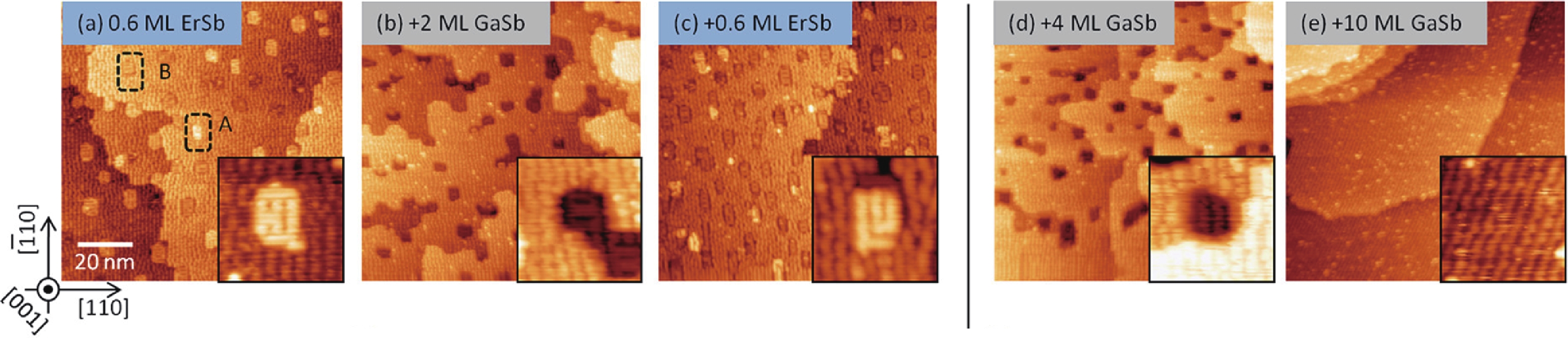
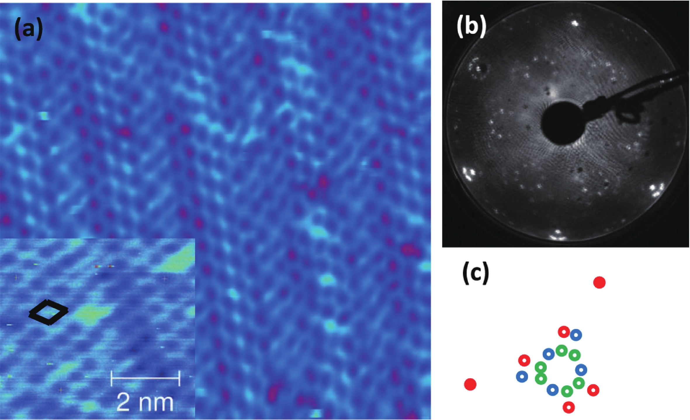
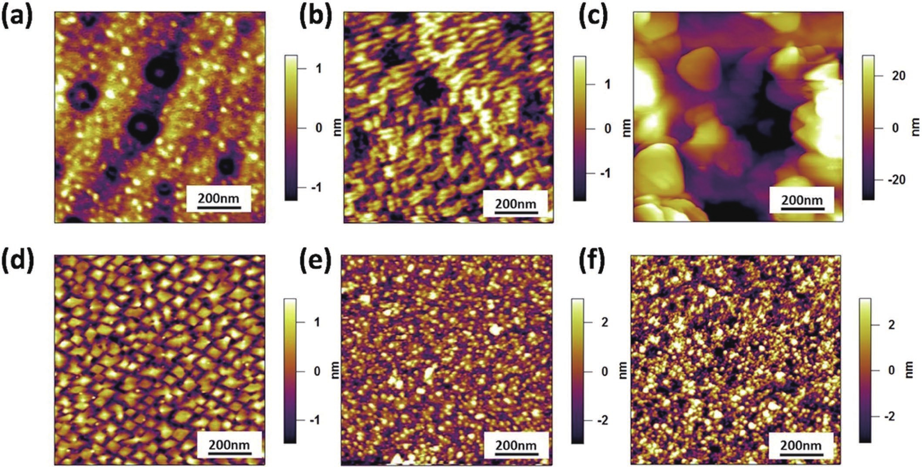
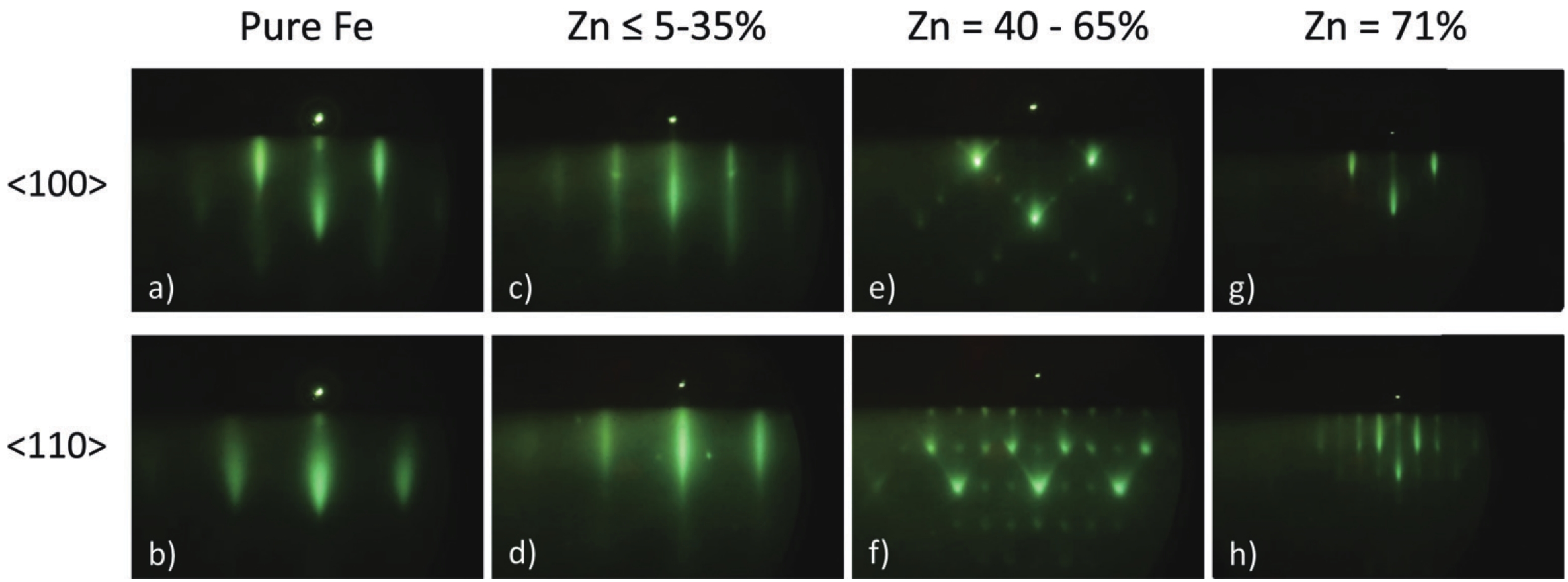
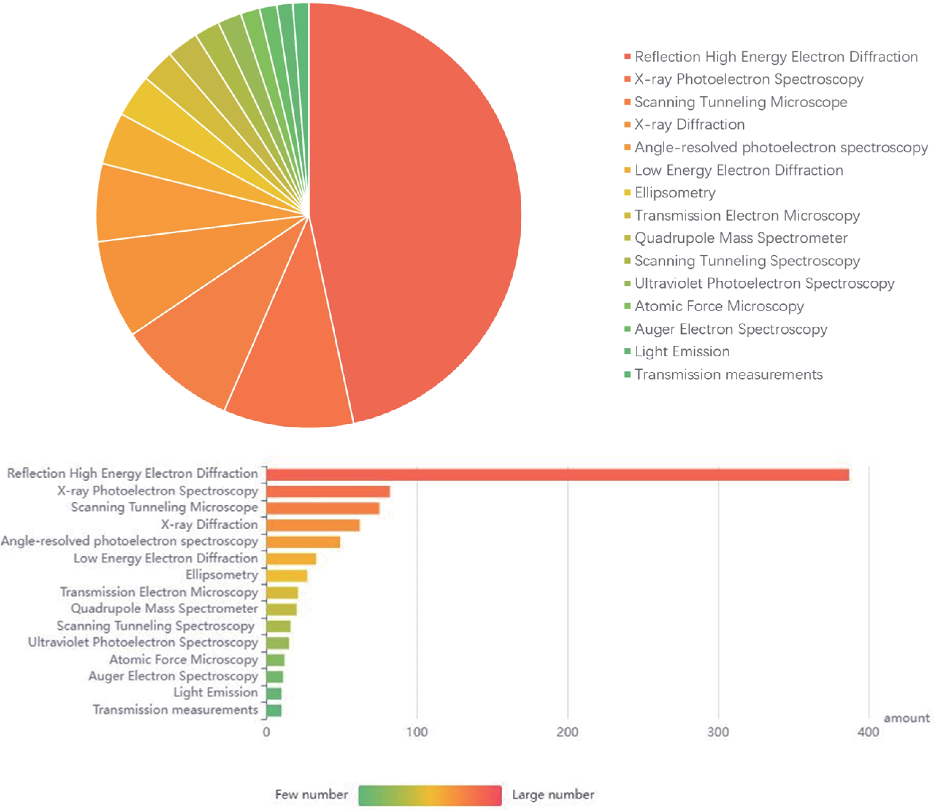
Table 1. A summary of the advantages, disadvantages, and functions of characterization technologies.
| Technique | Advantages | Disadvantages | Functions |
| STM | High spatial resolution; morphology and electronic structure analysis | Limited to conductive samples, requires ultra-high vacuum | Surface morphology, electronic structure analysis |
| SEM | High depth of field, for conductive and non-conductive samples | Lower resolution than STM, sample preparation challenges | Morphology analysis of various samples |
| AFM | High resolution in both lateral and vertical directions | Relatively slow imaging, tip wear and contamination effects | Surface morphology analysis, material property studies |
| LEEM | High spatial resolution, real-time imaging of surface dynamics | Limited to conductive samples, complex instrumentation | Surface morphology analysis, real-time imaging |
| RHEED | Real-time monitoring, provides crystal structure information | Limited to conducting samples, surface sensitivity variability | Thin-film growth monitoring, surface structure determination |
| LEED | High sensitivity for surface structure determination | Requires ultra-high vacuum, limited to ordered surfaces | Crystallography studies, surface structure analysis |
| GIFAD | Provides structural information for surfaces | Limited to specific incident angles, complex instrumentation | Surface structure analysis, studies of ordered surfaces |
| NFS | Nondestructive, element-specific, sensitive to vibrations | For certain isotopes, relatively low scattering cross section | Study of vibrational dynamics, element-specific analysis |
| RAS | Real-time monitoring, sensitive to surface changes | Requires careful data analysis, limited to specific materials | Monitoring of surface processes, surface structure analysis |
| XRS | Provides atomic arrangement information in crystals | Requires a crystalline sample, limited to periodic structures | Crystallography studies |
| XRD | High precision in determining crystal structures | For crystalline samples, bulk analysis lack surface specificity | Crystallography studies, analysis of crystalline materials |
| RSM | Detailed information on crystal lattice parameters | Requires crystalline samples, complex instrumentation | Strain analysis, determination of crystal lattice parameters |
| XANES | Provides local electronic structure information | For elements with absorption edges in the X-ray range | Study of local electronic structure in various materials |
| RS | Nondestructive, applicable to a wide range of materials | Low spatial resolution, susceptibility to fluorescence interference | molecular structures analysis |
| SE | High sensitivity, nondestructive | Requires accurate modeling, limited to certain sample types | Film thickness and optical constant determination |
| STM/STS | Provides electronic structure, density of states information | Limited to conductive samples, sample preparation challenges | Surface electronic structure, density of states analysis |
| QMS | High sensitivity to mass changes, real-time analysis | Limited to gas-phase analysis, may require sample ionization | Gas composition analysis |
| DMS | Provides real-time information on desorbed species analysis | Limited to studying desorption phenomena, sample-dependent | Surface desorption analysis, study of desorption processes |
| PES | High surface sensitivity, elemental composition analysis | Requires ultra-high vacuum, limited to surface analysis | Surface composition analysis, chemical state determination |
| XPS | Surface-sensitive for elemental composition analysis | Limited depth of analysis, sample charging affect results | Surface composition analysis, chemical state determination |
| UPS | Provides information about valence band, surface-sensitive | Requires ultra-high vacuum, limited to surface analysis | Valence band electronic structure analysis, surface chemical analysis |
| ARPES | Provides detailed information about electronic band structure | Requires ultra-high vacuum, limited to surface analysis | Electronic band structure analysis, surface electronic states |
| CEMS | Provides information on chemical environment, Mössbauer-active nuclei | Limited to specific isotopes, requires cryogenic temperatures | Study of chemical environments, Mössbauer-active nuclei analysis |
| MOKE | Sensitive to magnetic properties and domain structures | Limited to magnetic materials, complex instrumentation | Magnetic domain structure, magnetic properties analysis |
| XAS | Provides information on local electronic and geometric structure | Requires synchrotron radiation, complex data analysis | Local electronic and geometric structure analysis |
| XPD | Provides structural information at the atomic level, surface-sensitive | Requires ultra-high vacuum, limited to surface analysis | Surface structural analysis, study of atomic arrangement |
| AES | Elemental and chemical state analysis of surfaces, high sensitivity | Limited depth of analysis, surface sensitivity | Surface composition analysis, chemical state determination |
| EELS | Provides information on electronic excitations and bonding, high spatial resolution | Requires sophisticated instrumentation, complex data analysis | Electronic structure analysis, study of electronic excitations |
| AIPES | Provides angle-integrated information on electronic structure | Limited to angle-integrated data, lack angular information | Electronic structure analysis, study of electronic states |
| CM | Measures surface curvature, provides strain information | Limited to surface properties | Strain analysis, characterization of curved surfaces |
| MOS | Simultaneous measurement of multiple parameters | System complexity may require careful calibration | Multifaceted parameter monitoring, simultaneous data acquisition |
| 4PC | Accurate measurement of electrical conductivity | Requires precise sample preparation | Electrical conductivity analysis, study of conductive materials |
| BEM | Monitors changes in band structure during processes | Specific to semiconductor materials, requires precise control of growth conditions | Real-time monitoring of band structure changes during thin-film growth |
| XPEEM | Combines high-resolution imaging with surface-sensitive spectroscopy | Requires ultra-high vacuum conditions, limited to surface analysis | Surface chemical composition analysis, electronic structure imaging |
| CL | Probes luminescent properties of materials under electron beam excitation | Limited to materials with luminescent properties, resolution may be limited | Study of bandgap, defects, and luminescent properties of materials |
| XMCD | Sensitive to magnetic properties and magnetic moments of elements | Requires synchrotron radiation for high-quality data, limited to magnetic materials | Study of magnetic properties, magnetic moment determination |
| DRS | Sensitive to changes in the optical properties of materials | Data analysis may require careful consideration of multiple factors | Monitoring changes in optical properties, surface and interface analysis |
 DownLoad: CSV
| [1] |
Nunn W, Truttmann T K, Jalan B. A review of molecular-beam epitaxy of wide bandgap complex oxide semiconductors. J Mater Res, 2021, 36, 4846 doi: 10.1557/s43578-021-00377-1
|
| [2] |
Zuo Z, Xu Z G, Zheng R J, et al. In-situ epitaxial growth of graphene/h-BN van der Waals heterostructures by molecular beam epitaxy. Sci Rep, 2015, 5, 14760 doi: 10.1038/srep14760
|
| [3] |
Zhao C, Ng T K, Wei N N, et al. Facile formation of high-quality InGaN/GaN quantum-disks-in-nanowires on bulk-metal substrates for high-power light-emitters. Nano Lett, 2016, 16, 1056 doi: 10.1021/acs.nanolett.5b04190
|
| [4] |
Priante D, Janjua B, Prabaswara A, et al. Highly uniform ultraviolet-a quantum-confined AlGaN nanowire LEDs on metal/silicon with a TaN interlayer. Opt Mater Express, 2017, 7, 4214 doi: 10.1364/OME.7.004214
|
| [5] |
Zhao C, Chen Y H, Xu B, et al. Evolution of InAs nanostructures grown by droplet epitaxy. Appl Phys Lett, 2007, 91, 033112 doi: 10.1063/1.2757151
|
| [6] |
Bollinger A T, Wu J, Božović I. Perspective: Rapid synthesis of complex oxides by combinatorial molecular beam epitaxy. APL Mater, 2016, 4, 053205 doi: 10.1063/1.4943989
|
| [7] |
Kim H S, Jeong J, Kwon G H, et al. Improvement of electrical performance using PtSe2/PtTe2 edge contact synthesized by molecular beam epitaxy. Appl Surf Sci, 2022, 585, 152507 doi: 10.1016/j.apsusc.2022.152507
|
| [8] |
Ma Y F, Zhang S C, Peng Z F, et al. Investigation on 1065 nm laser performance with Nd: GdLaNbO4 mixed crystal and molybdenum disulfide. Opt Laser Technol, 2019, 120, 105715 doi: 10.1016/j.optlastec.2019.105715
|
| [9] |
Bourree L E, Chasse D R, Stephan Thamban P L, et al. Comparison of the optical characteristics of GaAs photocathodes grown using MBE and MOCVDSPIE Proceedings. Low-Light-Level and Real-Time Imaging Systems, Components, and Applications. 2003, 11
|
| [10] |
Schubert F, Zybell S, Heitmann J, et al. Influence of the substrate grade on structural and optical properties of GaN/AlGaN superlattices. J Cryst Growth, 2015, 425, 145 doi: 10.1016/j.jcrysgro.2015.02.037
|
| [11] |
Opel M. Spintronic oxides grown by laser-MBE. J Phys D: Appl Phys, 2012, 45, 033001 doi: 10.1088/0022-3727/45/3/033001
|
| [12] |
Kosiel K. MBE—Technology for nanoelectronics. Vacuum, 2008, 82, 951 doi: 10.1016/j.vacuum.2008.01.033
|
| [13] |
Zekentes K, Papaioannou V, Pecz B, et al. Early stages of growth of β-SiC on Si by MBE. J Cryst Growth, 1995, 157, 392 doi: 10.1016/0022-0248(95)00330-4
|
| [14] |
Güsken N A, Rieger T, Zellekens P, et al. MBE growth of Al/InAs and Nb/InAs superconducting hybrid nanowire structures. Nanoscale, 2017, 9, 16735 doi: 10.1039/C7NR03982D
|
| [15] |
Iha H, Hirota Y, Yamauchi M, et al. Effect of arsenic cracking on in incorporation into MBE-grown InGaAs layer. Phys Status Solidi C, 2015, 12, 524 doi: 10.1002/pssc.201400286
|
| [16] |
Zhu K J, Bai Y H, Hong X Y, et al. Investigating and manipulating the molecular beam epitaxy growth kinetics of intrinsic magnetic topological insulator MnBi2Te4 with in situ angle-resolved photoemission spectroscopy. J Phys: Condens Matter, 2020, 32, 475002 doi: 10.1088/1361-648X/aba06d
|
| [17] |
Fan J Q, Wang S Z, Yu X Q, et al. Molecular beam epitaxy growth and surface structure of Sr1– x Nd x CuO2 cuprate films. Phys Rev B, 2020, 101, 180508 doi: 10.1103/PhysRevB.101.180508
|
| [18] |
Marin D V, Shvets V A, Azarov I A, et al. Ellipsometric thermometry in molecular beam epitaxy of mercury cadmium telluride. Infrared Phys Technol, 2021, 116, 103793 doi: 10.1016/j.infrared.2021.103793
|
| [19] |
Hilse M, Wang X Y, Killea P, et al. Spectroscopic ellipsometry as an in situ monitoring tool for Bi2Se3 films grown by molecular beam epitaxy. J Cryst Growth, 2021, 566/567, 126177 doi: 10.1016/j.jcrysgro.2021.126177
|
| [20] |
Botchkarev A, Salvador A, Sverdlov B, et al. Properties of GaN films grown under Ga and N rich conditions with plasma enhanced molecular beam epitaxy. J Appl Phys, 1995, 77, 4455 doi: 10.1063/1.359474
|
| [21] |
Peng H S, Li Q W, Chen T. Preface. Industrial applications of carbon nanotubes. Amsterdam: Elsevier, 2017
|
| [22] |
Karpov S Y, Talalaev R A, Makarov Y N, et al. Surface kinetics of GaN evaporation and growth by molecular-beam epitaxy. Surf Sci, 2000, 450, 191 doi: 10.1016/S0039-6028(00)00055-8
|
| [23] |
Mudiyanselage K, Katsiev K, Idriss H. Effects of experimental parameters on the growth of GaN nanowires on Ti-film/Si(1 0 0) and Ti-foil by molecular beam epitaxy. J Cryst Growth, 2020, 547, 125818 doi: 10.1016/j.jcrysgro.2020.125818
|
| [24] |
Jung Y W, Kim T J, Kim Y D, et al. Temperature dependence of the dielectric response of AlSb. AIP Conference Proceedings, 2011, 37 doi: 10.1063/1.3666246
|
| [25] |
Albert M, Golla C, Meier C. Optical in situ temperature management for high-quality ZnO molecular beam epitaxy. J Cryst Growth, 2021, 557, 126009 doi: 10.1016/j.jcrysgro.2020.126009
|
| [26] |
Fortin-Deschênes M, Waller O, Menteş T O, et al. Synthesis of antimonene on germanium. Nano Lett, 2017, 17, 4970 doi: 10.1021/acs.nanolett.7b02111
|
| [27] |
Zhang W, Enriquez H, Mayne A J, et al. First steps of blue phosphorene growth on Au(1 1 1). Mater Today, 2021, 39, 1153
|
| [28] |
Wang W, Zhou Q A, Dong Y A, et al. Critical thickness for strain relaxation of Ge1– x Sn x ( x ≤ 0.17) grown by molecular beam epitaxy on Ge(001). Appl Phys Lett, 2015, 106, 232106 doi: 10.1063/1.4922529
|
| [29] |
Kong Y, Bennett C J, Hyde C J. A review of non-destructive testing techniques for the in situ investigation of fretting fatigue cracks. Mater Des, 2020, 196, 109093 doi: 10.1016/j.matdes.2020.109093
|
| [30] |
Lin H J, Li H W, Shao H Y, et al. In situ measurement technologies on solid-state hydrogen storage materials: A review. Mater Today Energy, 2020, 17, 100463 doi: 10.1016/j.mtener.2020.100463
|
| [31] |
Zhernokletov D M, Dong H, Brennan B, et al. Investigation of arsenic and antimony capping layers, and half cycle reactions during atomic layer deposition of Al2O3 on GaSb(100). J Vac Sci Technol A, 2013, 31, 060602
|
| [32] |
Laukkanen P, Punkkinen M P J, Lång J J K, et al. Bismuth-containing c(4 × 4) surface structure of the GaAs(1 0 0) studied by synchrotron-radiation photoelectron spectroscopy and ab initio calculations. J Electron Spectrosc Relat Phenom, 2014, 193, 34 doi: 10.1016/j.elspec.2014.02.008
|
| [33] |
Zhang W, Wong P K J, Jiang S, et al. Integrating spin-based technologies with atomically controlled van der Waals interfaces. Mater Today, 2021, 51, 350 doi: 10.1016/j.mattod.2021.09.015
|
| [34] |
Lazarenko A A, Berezovskaya T N, Denisov D V, et al. Preparation of a silicon surface for subsequent growth of dilute nitride alloys by molecular-beam epitaxy. J Phys, 2017, 917, 32003 doi: 10.1088/1742-6596/917/3/032003
|
| [35] |
Kladko V, Kuchuk A, Lytvyn P, et al. Substrate effects on the strain relaxation in GaN/AlN short-period superlattices. Nanoscale Res Lett, 2012, 7, 289 doi: 10.1186/1556-276X-7-289
|
| [36] |
Zhang T, Levy N, Ha J, et al. Scanning tunneling microscopy of gate tunable topological insulator Bi2Se3 thin films. Phys Rev B, 2013, 87, 115410 doi: 10.1103/PhysRevB.87.115410
|
| [37] |
Bai A F, Hilse M, Patil P D, et al. Probing the growth quality of molecular beam epitaxy-grown Bi2Se3 films via in situ spectroscopic ellipsometry. J Cryst Growth, 2022, 591, 126714 doi: 10.1016/j.jcrysgro.2022.126714
|
| [38] |
Lin W Z, Foley A, Alam K, et al. Facility for low-temperature spin-polarized-scanning tunneling microscopy studies of magnetic/spintronic materials prepared in situ by nitride molecular beam epitaxy. Rev Sci Instrum, 2014, 85, 043702 doi: 10.1063/1.4870276
|
| [39] |
Huidobro J, Aramendia J, Arana G, et al. Reviewing in situ analytical techniques used to research Martian geochemistry: From the Viking project to the MMX future mission. Anal Chim Acta, 2022, 1197, 339499 doi: 10.1016/j.aca.2022.339499
|
| [40] |
Lin D M, Li K K, Zhou L M. Advanced in situ characterizations of nanocomposite electrodes for sodium-ion batteries-A short review. Compos Commun, 2021, 25, 100635 doi: 10.1016/j.coco.2021.100635
|
| [41] |
O'Hegarty R, Kinnane O, Lennon D, et al. In-situ U-value monitoring of highly insulated building envelopes: Review and experimental investigation. Energy Build, 2021, 252, 111447 doi: 10.1016/j.enbuild.2021.111447
|
| [42] |
Socha R P, Szczepanik-Ciba M, Powroźnik W, et al. Epitaxial α-Mn(001) films on MgO(001). Thin Solid Films, 2014, 556, 137 doi: 10.1016/j.tsf.2014.01.050
|
| [43] |
Yang R, Krzyzewski T, Jones T. The study of in situ scanning tunnelling microscope characterization on GaN thin film grown by plasma assisted molecular beam epitaxy. Appl Phys Lett, 2013, 102, 112104 doi: 10.1063/1.4795790
|
| [44] |
Kawasaki J K, Schultz B D, Lu H, et al. Surface-mediated tunable self-assembly of single crystal semimetallic ErSb/GaSb nanocomposite structures. Nano Lett, 2013, 13, 2895 doi: 10.1021/nl4012563
|
| [45] |
Hernández-Rodríguez I, García J M, Martín-Gago J A, et al. Graphene growth on Pt(111) and Au(111) using a MBE carbon solid-source. Diam Relat Mater, 2015, 57, 58 doi: 10.1016/j.diamond.2015.03.004
|
| [46] |
Haze M, Torii Y, Peters R, et al. In situ STM observation of nonmagnetic impurity effect in MBE-grown CeCoIn5 films. J Phys Soc Jpn, 2018, 87, 034702 doi: 10.7566/JPSJ.87.034702
|
| [47] |
Cai X Q, Xu Z L, Zhou H, et al. Epitaxial growth and band structure of antiferromagnetic Mott insulator CeOI. Phys Rev Materials, 2020, 4, 064003 doi: 10.1103/PhysRevMaterials.4.064003
|
| [48] |
Dávila M E, Xian L, Cahangirov S, et al. Germanene: A novel two-dimensional germanium allotrope akin to graphene and silicene. New J Phys, 2014, 16, 095002 doi: 10.1088/1367-2630/16/9/095002
|
| [49] |
Allongue P, Maroun F. Electrodeposited magnetic layers in the ultrathin limit. MRS Bull, 2010, 35, 761 doi: 10.1557/mrs2010.505
|
| [50] |
Wu Z B, Putzky D, Kundu A K, et al. Homogeneous superconducting gap in DyBa2Cu3O7– δ synthesized by oxide molecular beam epitaxy. Phys Rev Materials, 2020, 4, 124801 doi: 10.1103/PhysRevMaterials.4.124801
|
| [51] |
Song C L, Wang Y L, Jiang Y P, et al. Topological insulator Bi2Se3 thin films grown on double-layer graphene by molecular beam epitaxy. Appl Phys Lett, 2010, 97, 143118 doi: 10.1063/1.3494595
|
| [52] |
Toujyou T, Tsukamoto S. Temperature-dependent site control of InAs/GaAs (001) quantum dots using a scanning tunneling microscopy tip during growth. Nanoscale Res Lett, 2010, 5, 1930 doi: 10.1007/s11671-010-9802-z
|
| [53] |
Toujyou T, Tsukamoto S. in situ STM observation during InAs growth in nano holes at 300 °C. Surf Sci, 2011, 605, 1320 doi: 10.1016/j.susc.2011.04.026
|
| [54] |
Rauschenbach B, Lotnyk A, Neumann L, et al. Ion beam assisted deposition of thin epitaxial GaN films. Materials, 2017, 10, 690 doi: 10.3390/ma10070690
|
| [55] |
Nishinaga T. Handbook of crystal growth (Second Edition). Boston: Elsevier, 2015
|
| [56] |
Kolíbal M, Pejchal T, Musálek T, et al. Catalyst–substrate interaction and growth delay in vapor–liquid–solid nanowire growth. Nanotechnology, 2018, 29, 205603 doi: 10.1088/1361-6528/aab474
|
| [57] |
Wang K, Yamaguchi T, Araki T, et al. In situ investigation of growth mechanism during molecular beam epitaxy of In-polar InN. Jpn J Appl Phys, 2011, 50, 01AE02 doi: 10.7567/JJAP.50.01AE02
|
| [58] |
Kim J, Hou B Y, Park C, et al. Effect of defects on reaction of NiO surface with Pb-contained solution. Sci Rep, 2017, 7, 44805 doi: 10.1038/srep44805
|
| [59] |
Deng H B, Li Y A, Feng Z L, et al. Moiré superlattice modulations in single-unit-cell FeTe films grown on NbSe2 single crystals. Chin Phys B, 2021, 30, 126801 doi: 10.1088/1674-1056/ac0816
|
| [60] |
Sutter P, Sutter E. Growth mechanisms of anisotropic layered group IV chalcogenides on van der waals substrates for energy conversion applications. ACS Appl Nano Mater, 2018, 1, 3026 doi: 10.1021/acsanm.8b00660
|
| [61] |
Fortin-Deschênes M, Moutanabbir O. Recovering the semiconductor properties of the epitaxial group V 2D materials antimonene and arsenene. J Phys Chem C, 2018, 122, 9162 doi: 10.1021/acs.jpcc.8b00044
|
| [62] |
Kanjanachuchai S, Wongpinij T, Kijamnajsuk S, et al. Preferential nucleation, guiding, and blocking of self-propelled droplets by dislocations. J Appl Phys, 2018, 123, 161570 doi: 10.1063/1.5008784
|
| [63] |
Mandziak A, Soria G D, Prieto J E, et al. Different spin axis orientation and large antiferromagnetic domains in Fe-doped NiO/Ru(0001) epitaxial films. Nanoscale, 2020, 12, 21225 doi: 10.1039/D0NR05756H
|
| [64] |
Croes B, Cheynis F, Müller P, et al. Polar surface of ferroelectric nanodomains in GeTe thin films. Phys Rev Materials, 2022, 6, 064407 doi: 10.1103/PhysRevMaterials.6.064407
|
| [65] |
Bag A, Das S, Biswas D. Observation of in-situ reciprocal lattice evolution of AlGaN/InGaN on Si (111) through GaN and AlN interlayers by RHEED and reflectance. Phys Status Solidi C, 2016, 13, 186 doi: 10.1002/pssc.201510202
|
| [66] |
Guo W, Ji D X, Yuan Z S, et al. Epitaxial growth of bronze phase titanium dioxide by molecular beam epitaxy. AIP Adv, 2019, 9, 035230 doi: 10.1063/1.5089906
|
| [67] |
Zhou H, Liao X X, Ke S M. Effects of strain on ultrahigh-performance optoelectronics and growth behavior of high-quality indium tin oxide films on yttria-stabilized zirconia (001) substrates. J Mater Sci, 2021, 32, 21462 doi: 10.1007/s10854-021-06654-3
|
| [68] |
Ghosh K, Busi P, Das S, et al. Excimer laser annealing: An alternative route and its optimisation to effectively activate Si dopants in AlN films grown by plasma assisted molecular beam epitaxy. Mater Res Bull, 2018, 97, 300 doi: 10.1016/j.materresbull.2017.09.016
|
| [69] |
Zhu J, Jing J, Luo W B, et al. Epitaxial growth of (100)-oriented ceria film on c-plane GaN/Al2O3 using YSZ/TiO2 buffer layers by pulse laser molecular beam epitaxy. J Vac Sci Technol B, 2011, 29, 032202 doi: 10.1116/1.3574523
|
| [70] |
Strawbridge B, Cernetic N, Chapley J, et al. Influence of surface topography on in situ reflection electron energy loss spectroscopy plasmon spectra of AlN, GaN, and InN semiconductors. J Vac Sci Technol A, 2011, 29, 041602 doi: 10.1116/1.3584775
|
| [71] |
Alanís A, Vilchis H, López E, et al. Cubic GaN films grown below the congruent sublimation temperature of (0 0 1) GaAs substrates by plasma-assisted molecular beam epitaxy. J Vac Sci Technol B, 2016, 34, 02L115 doi: 10.1116/1.4943661
|
| [72] |
Pak J, Lin W, Wang K, et al. Growth of epitaxial iron nitride ultrathin film on zinc-blende gallium nitride. J Vac Sci Technol A, 2010, 28, 536 doi: 10.1116/1.3425805
|
| [73] |
Li Y P, Wang H Q, Zhou H, et al. Tuning the surface morphologies and properties of ZnO films by the design of interfacial layer. Nanoscale Res Lett, 2017, 12, 551 doi: 10.1186/s11671-017-2301-8
|
| [74] |
Li Q, Ying M J, Zhang M D, et al. Structural characterization and surface polarity determination of polar ZnO films prepared by MBE. Appl Nanosci, 2023, 13, 3197 doi: 10.1007/s13204-021-01978-2
|
| [75] |
Dau M T, Petit M, Watanabe A, et al. Growth of germanium nanowires on silicon(111) substrates by molecular beam epitaxy. J Nanosci Nanotech, 2011, 11, 9292 doi: 10.1166/jnn.2011.4288
|
| [76] |
Ge F F, Wang X M, Li Y N, et al. Controllable growth of nanocomposite films with metal nanocrystals sandwiched between dielectric superlattices. J Nanopart Res, 2011, 13, 6447 doi: 10.1007/s11051-011-0475-z
|
| [77] |
Mietze C, DeCuir E A Jr, Manasreh M O, et al. Inter- and intrasubband spectroscopy of cubic AlN/GaN superlattices grown by molecular beam epitaxy on 3C-SiC. Phys Status Solidi (c), 2010, 7, 64 doi: 10.1002/pssc.200982612
|
| [78] |
Yang Z, Ke C, Sun L L, et al. Growth and structure investigation of multiferroic superlattices: [(La0.8Sr0.2MnO3)4n/(BaTiO3)3n]M. Solid State Commun, 2010, 150, 1432 doi: 10.1016/j.ssc.2010.05.022
|
| [79] |
Kwoen J, Arakawa Y. Classification of reflection high-energy electron diffraction pattern using machine learning. Cryst Growth Des, 2020, 20, 5289 doi: 10.1021/acs.cgd.0c00506
|
| [80] |
Haislmaier R C, Stone G, Alem N, et al. Creating Ruddlesden-Popper phases by hybrid molecular beam epitaxy. Appl Phys Lett, 2016, 109, 043102 doi: 10.1063/1.4959180
|
| [81] |
McClure A, Rugheimer P, Idzerda Y U. Magnetic and structural properties of single crystal Fe1– x Znx thin films. J Appl Phys, 2011, 109, 07A932 doi: 10.1063/1.3561079
|
| [82] |
Halder N, Suseendran J, Chakrabarti S, et al. Effect of InAlGaAs and GaAs combination barrier thickness on the duration of dot formation in different layers of stacked InAs/GaAs quantum dot heterostructure grown by MBE. J Nanosci Nanotech, 2010, 10, 5202 doi: 10.1166/jnn.2010.2380
|
| [83] |
Zhao J E, Zeng Y P, Liu C, et al. Substrate temperature dependence of ZnTe epilayers grown on GaAs(001) by molecular beam epitaxy. J Cryst Growth, 2010, 312, 1491 doi: 10.1016/j.jcrysgro.2010.01.032
|
| [84] |
Ma Y, Edgeton A, Paik H, et al. Realization of epitaxial thin films of the topological crystalline insulator Sr3SnO. Advanced Materials, 2020, 32(34), 2000809 doi: 10.1002/adma.202000809
|
| [85] |
Encomendero J, Islam S M, Jena D, et al. Molecular beam epitaxy of polar III-nitride resonant tunneling diodes. J Vac Sci Technol A, 2021, 39, 023409 doi: 10.1116/6.0000775
|
| [86] |
Dursap T, Vettori M, Botella C, et al. Wurtzite phase control for self-assisted GaAs nanowires grown by molecular beam epitaxy. Nanotechnology, 2021, 32, 155602 doi: 10.1088/1361-6528/abda75
|
| [87] |
Debiossac M, Atkinson P, Zugarramurdi A, et al. Fast atom diffraction inside a molecular beam epitaxy chamber, a rich combination. Appl Surf Sci, 2017, 391, 53 doi: 10.1016/j.apsusc.2016.02.157
|
| [88] |
Schöffmann P, Pütter S, Schubert J, et al. Tuning the Co/Sr stoichiometry of SrCoO2.5 thin films by RHEED assisted MBEgrowth. Mater Res Express, 2020, 7, 116404 doi: 10.1088/2053-1591/abc58b
|
| [89] |
Nechaev D V, Sitnikova A A, Brunkov P N, et al. Stress generation and relaxation in (Al, Ga)N/6H-SiC heterostructure grown by plasma-assisted molecular-beam epitaxy. Tech Phys Lett, 2017, 43, 443 doi: 10.1134/S106378501705008X
|
| [90] |
Zolotukhin D, Nechaev D, Kuznetsova N, et al. Control of stress and threading dislocation density in the thick GaN/AlN buffer layers grown on Si (111) substrates by low- temperature MBE. J Phys:Conf Ser, 2016, 741, 012025 doi: 10.1088/1742-6596/741/1/012025
|
| [91] |
Vogt P, Bierwagen O. The competing oxide and sub-oxide formation in metal-oxide molecular beam epitaxy. Appl Phys Lett, 2015, 106, 081910 doi: 10.1063/1.4913447
|
| [92] |
Jakob J, Schroth P, Feigl L, et al. Correlating in situ RHEED and XRD to study growth dynamics of polytypism in nanowires. Nanoscale, 2021, 13, 13095 doi: 10.1039/D1NR02320A
|
| [93] |
Sen S, Paul S, Singha C, et al. Monitoring the growth of III-nitride materials by plasma assisted molecular beam epitaxy employing diffuse scattering of RHEED. J Vac Sci Technol B, 2020, 38, 014007 doi: 10.1116/1.5124048
|
| [94] |
May B J, Kim J J, Walker P, et al. Molecular beam epitaxy of GaAs templates on water soluble NaCl thin films. J Cryst Growth, 2022, 586, 126617 doi: 10.1016/j.jcrysgro.2022.126617
|
| [95] |
Keenan C, Chandril S, Myers T H, et al. In-situ stoichiometry determination using X-ray fluorescence generated by reflection-high-energy-electron-diffraction. J Appl Phys, 2011, 109, 114305 doi: 10.1063/1.3592219
|
| [96] |
Provence S R, Thapa S, Paudel R, et al. Machine learning analysis of perovskite oxides grown by molecular beam epitaxy. Phys Rev Materials, 2020, 4, 083807 doi: 10.1103/PhysRevMaterials.4.083807
|
| [97] |
Kwoen J, Arakawa Y. Classification of in situ reflection high energy electron diffraction images by principal component analysis. Jpn J Appl Phys, 2021, 60, SBBK03 doi: 10.35848/1347-4065/abdad5
|
| [98] |
Yanilkin I, Mohammed W, Gumarov A, et al. Synthesis, characterization, and magnetoresistive properties of the epitaxial Pd0.96Fe0.04/VN/Pd0.92Fe0.08 superconducting spin-valve heterostructure. Nanomaterials, 2020, 11, 64 doi: 10.3390/nano11010064
|
| [99] |
Carpenter M. A, Mathur S, Kolmakov A. Metal oxide nanomaterials for chemical sensors. Springer, 2013
|
| [100] |
Kuschel O, Spiess W, Schemme T, et al. Real-time monitoring of the structure of ultrathin Fe3O4 films during growth on Nb-doped SrTiO3(001). Appl Phys Lett, 2017, 111, 041902 doi: 10.1063/1.4995408
|
| [101] |
Esmaeili A, Yanilkin I V, Gumarov A I, et al. Epitaxial growth of Pd1− x Fe x films on MgO single-crystal substrate. Thin Solid Films, 2019, 669, 338 doi: 10.1016/j.tsf.2018.11.015
|
| [102] |
Zhang L, Shi D X, Du S X, et al. Structural transition and thermal stability of a coronene molecular monolayer on Cu(110). J Phys Chem C, 2010, 114, 11180 doi: 10.1021/jp101865j
|
| [103] |
Ruwisch K, Pohlmann T, Hoppe M, et al. Inferface magnetization phenomena in epitaxial thin Fe3O4/Co x Fe3– x O4 bilayers. J Phys Chem C, 2021, 125, 23327 doi: 10.1021/acs.jpcc.1c05274
|
| [104] |
Navío C, Villanueva M, Céspedes E, et al. Ultrathin films of L1-MnAl on GaAs (001): A hard magnetic MnAl layer onto a soft Mn-Ga-As-Al interface. APL Mater, 2018, 6, 101109 doi: 10.1063/1.5050852
|
| [105] |
Dhungana D S, Grazianetti C, Martella C, et al. Two-dimensional silicene–stanene heterostructures by epitaxy. Adv Funct Materials, 2021, 31, 2102797 doi: 10.1002/adfm.202102797
|
| [106] |
Hafez M A, Zayed M K, Elsayed-Ali H E. Review: Geometric interpretation of reflection and transmission RHEED patterns. Micron, 2022, 159, 103286 doi: 10.1016/j.micron.2022.103286
|
| [107] |
Debiossac M, Roncin P. Image processing for grazing incidence fast atom diffraction. Nucl Instrum Meth Phys Res Sect B, 2016, 382, 36 doi: 10.1016/j.nimb.2016.05.023
|
| [108] |
Debiossac M, Zugarramurdi A, Khemliche H, et al. Combined experimental and theoretical study of fast atom diffraction on the β2(2 × 4) reconstructed GaAs(001) surface. Phys Rev B, 2014, 90, 155308 doi: 10.1103/PhysRevB.90.155308
|
| [109] |
Merkel D G, Bessas D, Zolnai Z, et al. Evolution of magnetism on a curved nano-surface. Nanoscale, 2015, 7, 12878 doi: 10.1039/C5NR02928G
|
| [110] |
Knyazev Y V, Chumakov A I, Dubrovskiy A , et al. Nuclear forward scattering application to the spiral magnetic structure study in ε–Fe2O3. Phys Rev B, 2020, 101, 094408 doi: 10.1103/PhysRevB.101.094408
|
| [111] |
Strohm C, Van der Linden P, Rüffer R. Nuclear forward scattering of synchrotron radiation in pulsed high magnetic fields. Phys Rev Lett, 2010, 104, 087601 doi: 10.1103/PhysRevLett.104.087601
|
| [112] |
Gu R J, Shen C A, Guo Y Y, et al. in situ thickness and temperature measurements of CdTe grown by molecular beam epitaxy on GaAs substrate. J Vac Sci Technol B, 2012, 30, 041203 doi: 10.1116/1.4718777
|
| [113] |
Fleischer K, Verre R, Mauit O, et al. Reflectance anisotropy spectroscopy of magnetite (110) surfaces. Phys Rev B, 2014, 89, 195118 doi: 10.1103/PhysRevB.89.195118
|
| [114] |
Ortega-Gallegos J, Guevara-Macías L E, Lastras-Martínez A, et al. Rapid reflectance-anisotropy spectroscopy as an optical probe for real-time monitoring of thin film deposition. AIP Conference Proceedings, 2018, 1934, 040001 doi: 10.1063/1.5024494
|
| [115] |
Ortega-Gallegos J, Guevara-Macías L E, Ariza-Flores A D, et al. On the origin of reflectance-anisotropy oscillations during GaAs (0 0 1) homoepitaxy. Appl Surf Sci, 2018, 439, 963 doi: 10.1016/j.apsusc.2017.12.244
|
| [116] |
Cantelli V, Geaymond O, Ulrich O, et al. The in situ growth of nanostructures on surfaces (INS) endstation of the ESRF BM32 beamline: Acombined UHV–CVD and MBE reactor for in situ X-ray scattering investigations of growing nanoparticles and semiconductor nanowires. J Synchrotron Radiat, 2015, 22, 688 doi: 10.1107/S1600577515001605
|
| [117] |
Li Y, Wrobel F, Yan X, et al. Interface creation on a mixed-terminated perovskite surface. Appl Phys Lett, 2021, 118, 061601 doi: 10.1063/5.0036279
|
| [118] |
Kowarik S. Thin film growth studies using time-resolved X-ray scattering. J Phys:Condens Matter, 2017, 29, 043003 doi: 10.1088/1361-648X/29/4/043003
|
| [119] |
Andersen T K, Cook S, Wan G, et al. Layer-by-layer epitaxial growth of defect-engineered strontium cobaltites. ACS Appl Mater Interfaces, 2018, 10, 5949 doi: 10.1021/acsami.7b16970
|
| [120] |
Li Y, Wrobel F, Cheng Y J, et al. Self-healing growth of LaNiO3 on a mixed-terminated perovskite surface. ACS Appl Mater Interfaces, 2022, 14, 16928 doi: 10.1021/acsami.2c02357
|
| [121] |
Kakuda N, Kaizu T, Takahasi M, et al. Time-resolved X-ray diffraction measurements of high-density InAs quantum dots on Sb/GaAs layers and the suppression of coalescence by Sb-irradiated growth interruption. Jpn J Appl Phys, 2010, 49, 095602 doi: 10.1143/JJAP.49.095602
|
| [122] |
Takahasi M. X-ray diffraction study of crystal growth dynamics during molecular-beam epitaxy of III–V semiconductors. J Phys Soc Jpn, 2013, 82, 021011 doi: 10.7566/JPSJ.82.021011
|
| [123] |
Yan X, Wrobel F, Li Y, et al. in situ X-ray and electron scattering studies of oxide molecular beam epitaxial growth. APL Mater, 2020, 8, 101107 doi: 10.1063/5.0025849
|
| [124] |
Lee J H, Tung I C, Chang S H, et al. in situ surface/interface X-ray diffractometer for oxide molecular beam epitaxy. Rev Sci Instrum, 2016, 87, 013901 doi: 10.1063/1.4939100
|
| [125] |
Hong H, McChesney J L, Wrobel F, et al. in situ study on the evolution of atomic and electronic structure of LaTiO3/SrTiO3 system. Phys Rev Materials, 2022, 6, L011401 doi: 10.1103/PhysRevMaterials.6.L011401
|
| [126] |
Chakraborty J, Harzer T P, Duarte M J, et al. Phase decomposition in nanocrystalline Cr0.8Cu0.2 thin films. J Alloys Compd, 2021, 888, 161391 doi: 10.1016/j.jallcom.2021.161391
|
| [127] |
Diep N Q, Wu S K, Liu C W, et al. Pressure induced structural phase crossover of a GaSe epilayer grown under screw dislocation driven mode and its phase recovery. Sci Rep, 2021, 11, 19887 doi: 10.1038/s41598-021-99419-1
|
| [128] |
Sasaki T, Takahasi M. Influence of indium supply on Au-catalyzed InGaAs nanowire growth studied by in situ X-ray diffraction. J Cryst Growth, 2017, 468, 135 doi: 10.1016/j.jcrysgro.2016.11.113
|
| [129] |
Takahasi M. Quantitative monitoring of InAs quantum dot growth using X-ray diffraction. J Cryst Growth, 2014, 401, 372 doi: 10.1016/j.jcrysgro.2013.11.012
|
| [130] |
Mostafavi Kashani S M, Kriegner D, Bahrami D, et al. X-ray diffraction analysis of the angular stability of self-catalyzed GaAs nanowires for future applications in solar-light-harvesting and light-emitting devices. ACS Appl Nano Mater, 2019, 2, 689 doi: 10.1021/acsanm.8b01677
|
| [131] |
Sasaki T, Suzuki H, Sai A, et al. Growth temperature dependence of strain relaxation during InGaAs/GaAs(0 0 1) heteroepitaxy. J Cryst Growth, 2011, 323, 13 doi: 10.1016/j.jcrysgro.2010.10.005
|
| [132] |
Sasaki T, Takahasi M, Suzuki H, et al. in situ three-dimensional X-ray reciprocal-space mapping of InGaAs multilayer structures grown on GaAs(001) by MBE. J Cryst Growth, 2015, 425, 13 doi: 10.1016/j.jcrysgro.2015.03.044
|
| [133] |
Sasaki T, Takahasi M. Real-time structural analysis of InGaAs/InAs/GaAs(1 1 1)A interfaces by in situ synchrotron X-ray reciprocal space mapping. J Cryst Growth, 2019, 512, 33 doi: 10.1016/j.jcrysgro.2019.02.007
|
| [134] |
Ibrahimkutty S, Seiler A, Prüßmann T, et al. A portable ultrahigh-vacuum system for advanced synchrotron radiation studies of thin films and nanostructures: EuSi2nano-islands. J Synchrotron Radiat, 2015, 22, 91 doi: 10.1107/S1600577514019705
|
| [135] |
Wang C X, Zhu X G, Nilsson L, et al. in situ Raman spectroscopy of topological insulator Bi2Te3 films with varying thickness. Nano Res, 2013, 6, 688 doi: 10.1007/s12274-013-0344-4
|
| [136] |
Hutchins T, Nazari M, Eridisoorya M, et al. Raman measurements of substrate temperature in a molecular beam epitaxy growth chamber. Rev Sci Instrum, 2015, 86, 014904 doi: 10.1063/1.4905858
|
| [137] |
Fang Y R, Zhang Z L, Sun M T. High vacuum tip-enhanced Raman spectroscope based on a scanning tunneling microscope. Rev Sci Instrum, 2016, 87, 033104 doi: 10.1063/1.4943291
|
| [138] |
Jung Y W, Byun J S, Hwang S Y, et al. Dielectric response of AlP by in-situ ellipsometry. Thin Solid Films, 2011, 519, 8027 doi: 10.1016/j.tsf.2011.06.015
|
| [139] |
Johs B, He P. Substrate wobble compensation for in situ spectroscopic ellipsometry measurements. J Vac Sci Technol B, 2011, 29, 03C111 doi: 10.1116/1.3555332
|
| [140] |
Mi Z T, Wang L Z, Jagadish C. Preface. Semiconductors and semimetals. Elsevier, 2017
|
| [141] |
Voitsekhovskii A V, Nesmelov S N, Dzyadukh S M, et al. Electrical characterization of insulator-semiconductor systems based on graded band gap MBE HgCdTe with atomic layer deposited Al2O3 films for infrared detector passivation. Vacuum, 2018, 158, 136 doi: 10.1016/j.vacuum.2018.09.054
|
| [142] |
Mikhailov N, Shvets V, Ikusov D, et al. Interface studies in HgTe/HgCdTe quantum wells. Phys Status Solidi B, 2020, 257, 1900598 doi: 10.1002/pssb.201900598
|
| [143] |
Shvets V A, Mikhailov N N, Ikusov D G, et al. Determining the compositional profile of HgTe/Cd x Hg1– x Te quantum wells by single-wavelength ellipsometry. Opt Spectrosc, 2019, 127, 340 doi: 10.1134/S0030400X19080253
|
| [144] |
Tsukada M, Kobayashi K, Isshiki N, et al. First-principles theory of scanning tunneling microscopy. Surf Sci Rep, 1991, 13, 267 doi: 10.1016/0167-5729(91)90006-J
|
| [145] |
Koinuma H, Gonda S, Gong J P, et al. Surface and interface characterization of high Tc related epitaxial films by STM/STS and XPS. J Phys Chem Solids, 1993, 54, 1215 doi: 10.1016/0022-3697(93)90170-V
|
| [146] |
Dai J X, Wang W B, Brahlek M, et al. Restoring pristine Bi2Se3 surfaces with an effective Se decapping process. Nano Res, 2015, 8, 1222 doi: 10.1007/s12274-014-0607-8
|
| [147] |
Zhang L, Yang T, Sahdan M F, et al. Precise layer-dependent electronic structure of MBE-grown PtSe2. Adv Elect Materials, 2021, 7, 2100559 doi: 10.1002/aelm.202100559
|
| [148] |
Xue H Y, Yang H, Wu Y F, et al. Molecular beam epitaxy of superconducting PdTe2 films on topological insulator Bi2Te3. Sci China Phys Mech Astron, 2019, 62, 76801 doi: 10.1007/s11433-018-9342-3
|
| [149] |
Batey J H. The physics and technology of quadrupole mass spectrometers. Vacuum, 2014, 101, 410 doi: 10.1016/j.vacuum.2013.05.005
|
| [150] |
Sobanska M, Zytkiewicz Z R, Calabrese G, et al. Comprehensive analysis of the self-assembled formation of GaN nanowires on amorphous Al x O y : in situ quadrupole mass spectrometry studies. Nanotechnology, 2019, 30, 154002 doi: 10.1088/1361-6528/aafe17
|
| [151] |
Wölz M, Fernández-Garrido S, Hauswald C, et al. Indium incorporation in In x Ga1– x N/GaN nanowire heterostructures investigated by line-of-sight quadrupole mass spectrometry. Cryst Growth Des, 2012, 12, 5686 doi: 10.1021/cg301181b
|
| [152] |
Katmis F, Calarco R, Perumal K, et al. Insight into the growth and control of single-crystal layers of Ge–Sb–Te phase-change material. Cryst Growth Des, 2011, 11, 4606 doi: 10.1021/cg200857x
|
| [153] |
Auzelle T, Calabrese G, Fernández-Garrido S. Tuning the orientation of the top-facets of GaN nanowires in molecular beam epitaxy by thermal decomposition. Phys Rev Materials, 2019, 3, 013402 doi: 10.1103/PhysRevMaterials.3.013402
|
| [154] |
McCoy J, Lu C T, Kaspi R. in situ monitoring of GaSb1–xBi x growth using desorption mass spectrometry. J Vac Sci Technol B, 2020, 38, 022210 doi: 10.1116/1.5144687
|
| [155] |
Kaspi R, Lu C T, Yang C, et al. Desorption mass spectrometry: Revisiting the in situ calibration technique for mixed group-V alloy MBE growth of ~3.3 µm diode lasers. J Cryst Growth, 2015, 425, 5 doi: 10.1016/j.jcrysgro.2015.02.009
|
| [156] |
Thong Q N, Martin D M, Agham P, et al. Growth of crystalline LaAlO3 by atomic layer deposition. Proceedings Volume 8987, Oxide-based Materials and Devices V, 2014, 8987, 898712 doi: 10.1117/12.2045532
|
| [157] |
Lin Y H, Lin K Y, Hsueh W J, et al. Interfacial characteristics of Y2O3/GaSb(001) grown by molecular beam epitaxy and atomic layer deposition. J Cryst Growth, 2017, 477, 164 doi: 10.1016/j.jcrysgro.2017.02.038
|
| [158] |
Maiti P, Guha P, Hussain H, et al. Microscopy and spectroscopy study of nanostructural phase transformation from β-MoO3 to Mo under UHV - MBE conditions. Surf Sci, 2019, 682, 64 doi: 10.1016/j.susc.2018.12.008
|
| [159] |
Wu G G, Zheng W T, Gao F B, et al. Near infrared electroluminescence of ZnMgO/InN core-shell nanorod heterostructures grown on Si substrate. Phys Chem Chem Phys, 2016, 18, 20812 doi: 10.1039/C6CP03199D
|
| [160] |
Meng G, Ying H P, Wang X M, et al. Epitaxial growth and determination of the band alignment for Ni x Mg1- x O/MgO interface by laser molecular beam epitaxy. J Alloys Compd, 2020, 822, 153618 doi: 10.1016/j.jallcom.2019.153618
|
| [161] |
Han C, Xiang D, Zheng M R, et al. Tuning the electronic properties of ZnO nanowire field effect transistors via surface functionalization. Nanotechnology, 2015, 26, 095202 doi: 10.1088/0957-4484/26/9/095202
|
| [162] |
Wang X M, Yan D W, Shen C L, et al. Cu2O/MgO band alignment and Cu2O-Au nanocomposites with enhanced optical absorption. Opt Mater Express, 2013, 3, 1974 doi: 10.1364/OME.3.001974
|
| [163] |
Seo H, Choi M, Posadas A B, et al. Combined in-situ photoemission spectroscopy and density functional theory of the Sr Zintl template for oxide heteroepitaxy on Si(001). J Vac Sci Technol B, 2013, 31, 04D107 doi: 10.1116/1.4807716
|
| [164] |
Koster G, Rijnders G. In situ characterization of thin film growth. Woodhead Publishing Limited, 2011
|
| [165] |
Chatterjee S, Sung S H, Baek D J, et al. Epitaxial growth and electronic properties of mixed valence YbAl3 thin films. J Appl Phys, 2016, 120, 035105 doi: 10.1063/1.4958336
|
| [166] |
Kanagaraj M, Sun Y Z, Ning J A, et al. Topological quantum weak antilocalization limit and anomalous Hall effect in semimagnetic Bi2– x Cr x Se3/Bi2Se3– y Tey heterostructure. Mater Res Express, 2020, 7, 016401 doi: 10.1088/2053-1591/ab573f
|
| [167] |
Yang Y C, Liu Z T, Liu J S, et al. High-resolution ARPES endstation for in situ electronic structure investigations at SSRF. Nucl Sci Tech, 2021, 32, 31 doi: 10.1007/s41365-021-00858-2
|
| [168] |
Chatterjee S, Ruf J P, Wei H I, et al. Lifshitz transition from valence fluctuations in YbAl3. Nat Commun, 2017, 8, 852 doi: 10.1038/s41467-017-00946-1
|
| [169] |
Gong Y, Zhu K J, Li Z, et al. Experimental evidence of the thickness- and electric-field-dependent topological phase transitions in topological crystalline insulator SnTe(111) thin films. Nano Res, 2018, 11, 6045 doi: 10.1007/s12274-018-2120-y
|
| [170] |
Xiang P, Liu J S, Li M Y, et al. In situ electronic structure study of epitaxial niobium thin films by angle-resolved photoemission spectroscopy. Chin Phys Lett, 2017, 34, 077402 doi: 10.1088/0256-307X/34/7/077402
|
| [171] |
Zhou T, Tong M Y, Zhang Y, et al. Topological phase transition in Sb-doped Mg3Bi2 monocrystalline thin films. Phys Rev B, 2021, 103, 125405 doi: 10.1103/PhysRevB.103.125405
|
| [172] |
Liu Y, Nair H P, Ruf J P, et al. Revealing the hidden heavy Fermi liquid in CaRuO3. Phys Rev B, 2018, 98, 041110 doi: 10.1103/PhysRevB.98.041110
|
| [173] |
Huang Z C, Pu Y J, Xu H C, et al. Electronic structure and superconductivity of single-layer FeSe on Nb: SrTiO3/LaAlO3 with varied tensile strain. 2D Mater, 2016, 3, 014005 doi: 10.1088/2053-1583/3/1/014005
|
| [174] |
Abreu G J P, Paniago R, Pfannes H D. Growth of ultra-thin FeO(100) films on Ag(100): A combined XPS, LEED and CEMS study. J Magn Magn Mater, 2014, 349, 235 doi: 10.1016/j.jmmm.2013.08.059
|
| [175] |
Soria G D, Freindl K, Prieto J E, et al. Growth and characterization of ultrathin cobalt ferrite films on Pt(111). Appl Surf Sci, 2022, 586, 152672 doi: 10.1016/j.apsusc.2022.152672
|
| [176] |
Khalid N, Kim J Y, Ionescu A, et al. Structure and magnetic properties of an epitaxial Fe(110)/MgO(111)/GaN(0001) heterostructure. J Appl Phys, 2018, 123, 103901 doi: 10.1063/1.5022433
|
| [177] |
Li Y P, Wang H Q, Ibrahim K, et al. Interfacial electronic states of misfit heterostructure between hexagonal ZnO and cubic NiO. Phys Rev Materials, 2020, 4, 124601 doi: 10.1103/PhysRevMaterials.4.124601
|
| [178] |
Seiler A, Bauder O, Ibrahimkutty S, et al. Growth and structure characterization of EuSi2 films and nanoislands on vicinal Si(001) surface. J Cryst Growth, 2014, 407, 74 doi: 10.1016/j.jcrysgro.2014.09.005
|
| [179] |
Kilian A S, Bernardi F, Pancotti A, et al. Atomic structure of Cr2O3/Ag(111) and Pd/Cr2O3/Ag(111) surfaces: A photoelectron diffraction investigation. J Phys Chem C, 2014, 118, 20452 doi: 10.1021/jp506507e
|
| [180] |
Madisetti S, Tokranov V, Greene A, et al. Growth of strained InGaSb quantum wells for p-FET on Si: Defects, interfaces, and electrical properties. J Vac Sci Technol B, 2014, 32, 051206 doi: 10.1116/1.4892797
|
| [181] |
Zhang C M, Alberi K, Honsberg C, et al. Investigation of GaAs surface treatments for ZnSe growth by molecular beam epitaxy without a buffer layer. Appl Surf Sci, 2021, 549, 149245 doi: 10.1016/j.apsusc.2021.149245
|
| [182] |
Galkin N G, Galkin K N, Tupkalo A V, et al. A low temperature growth of Ca silicides on Si(100) and Si(111) substrates: Formation, structure, optical properties and energy band structure parameters. J Alloys Compd, 2020, 813, 152101 doi: 10.1016/j.jallcom.2019.152101
|
| [183] |
Peng R, Xu H C, Xia M, et al. Tuning the dead-layer behavior of La0.67Sr0.33MnO3/SrTiO3 via interfacial engineering. Appl Phys Lett, 2014, 104, 081606 doi: 10.1063/1.4866461
|
| [184] |
Fan C C, Liu Z T, Cai S H, et al. Reactive molecular beam epitaxial growth and in situ photoemission spectroscopy study of iridate superlattices. AIP Adv, 2017, 7, 085307 doi: 10.1063/1.4986429
|
| [185] |
Lingaparthi R, Dharmarasu N, Radhakrishnan K, et al. In-situ stress evolution and its correlation with structural characteristics of GaN buffer grown on Si substrate using AlGaN/AlN/GaN stress mitigation layers for high electron mobility transistor applications. Thin Solid Films, 2020, 708, 138128 doi: 10.1016/j.tsf.2020.138128
|
| [186] |
Aidam R, Diwo E, Rollbühler N, et al. Strain control of AlGaN/GaN high electron mobility transistor structures on silicon (111) by plasma assisted molecular beam epitaxy. J Appl Phys, 2012, 111, 114516 doi: 10.1063/1.4729045
|
| [187] |
Levillayer M, Arnoult A, Massiot I, et al. As-grown InGaAsN subcells for multijunction solar cells by molecular beam epitaxy. IEEE J Photovolt, 2021, 11, 1271 doi: 10.1109/JPHOTOV.2021.3093048
|
| [188] |
Cornille C, Arnoult A, Gravelier Q, et al. Links between bismuth incorporation and surface reconstruction during GaAsBi growth probed by in situ measurements. J Appl Phys, 2019, 126, 093106 doi: 10.1063/1.5111932
|
| [189] |
Nechaev D V, Koshelev O A, Ratnikov V V, et al. Effect of stoichiometric conditions and growth mode on threading dislocations filtering in AlN/ c-Al2O3 templates grown by PA MBE. Superlattices Microstruct, 2020, 138, 106368 doi: 10.1016/j.spmi.2019.106368
|
| [190] |
Hoefer K, Becker C, Rata D, et al. Intrinsic conduction through topological surface states of insulating Bi2Te3 epitaxial thin films. Proc Natl Acad Sci USA, 2014, 111, 14979 doi: 10.1073/pnas.1410591111
|
| [191] |
Jacobs R N, Pinkie B, Arias J, et al. In situ band-edge monitoring of Cd1−yZnyTe substrates for molecular beam epitaxy of HgCdTe. J Electron Mater, 2019, 48, 6138 doi: 10.1007/s11664-019-07354-9
|
| [192] |
Lo Y Y, Huang M F, Chiang Y C, et al. Effect of indium accumulation on the characteristics of a-plane InN epi-films under different growth conditions. Thin Solid Films, 2015, 589, 322 doi: 10.1016/j.tsf.2015.05.052
|
| [193] |
Mandziak A, de la Figuera J, Prieto J E, et al. Combining high temperature sample preparation and in situ magnetic fields in XPEEM. Ultramicroscopy, 2020, 214, 113010 doi: 10.1016/j.ultramic.2020.113010
|
| [194] |
Pereira V M, Wu C N, Liu C E, et al. Molecular beam epitaxy preparation and in situ characterization of FeTe thin films. Phys Rev Materials, 2020, 4, 023405 doi: 10.1103/PhysRevMaterials.4.023405
|
| [195] |
Mandziak A, de la Figuera J, Ruiz-Gómez S, et al. Structure and magnetism of ultrathin nickel-iron oxides grown on Ru(0001) by high-temperature oxygen-assisted molecular beam epitaxy. Sci Rep, 2018, 8, 17980 doi: 10.1038/s41598-018-36356-6
|
| [196] |
Sawada M, Ueno T, Tagashira T, et al. XMCD experimental station optimized for ultrathin magnetic films at HiSOR-BL14. AIP Conference Proceedings, 2010, 1234, 939 doi: DOI:10.1063/1.3463371
|
| [197] |
Forker R, Gruenewald M, Fritz T. Optical differential reflectance spectroscopy on thin molecular films. Annu Rep Prog Chem, Sect C: Phys Chem, 2012, 108, 34 doi: 10.1039/C2PC90002E
|
| [198] |
Jackson A W, Pinsukanjana P R, Gossard A C, et al. In situ monitoring and control for MBE growth of optoelectronic devices. IEEE J Sel Top Quantum Electron, 1997, 3, 836 doi: 10.1109/2944.640637
|
| [199] |
Das P, Halder N N, Kumar R, et al. Graded barrier AlGaN/AlN/GaN heterostructure for improved 2-dimensional electron gas carrier concentration and mobility. Electron Mater Lett, 2014, 10, 1087 doi: 10.1007/s13391-014-4067-9
|
| [200] |
Ogino T, Nishimura S, Shirakashi J I. Scratch nanolithography on Si surface using scanning probe microscopy: Influence of scanning parameters on groove size. Jpn J Appl Phys, 2008, 47, 712 doi: 10.1143/JJAP.47.712
|
| [201] |
Zhang L, Shao S F. Image-based machine learning for materials science. J Appl Phys, 2022, 132, 100701 doi: 10.1063/5.0087381
|
| [202] |
Liang H T, Stanev V, Kusne A G, et al. Application of machine learning to reflection high-energy electron diffraction images for automated structural phase mapping. Phys Rev Materials, 2022, 6, 063805 doi: 10.1103/PhysRevMaterials.6.063805
|


Article views: 1050 Times PDF downloads: 195 Times Cited by: 0 Times
Received: 29 July 2023 Revised: 13 November 2023 Online: Accepted Manuscript: 12 December 2023Uncorrected proof: 13 December 2023Published: 15 March 2024
| Citation: |
Chao Shen, Wenkang Zhan, Manyang Li, Zhenyu Sun, Jian Tang, Zhaofeng Wu, Chi Xu, Bo Xu, Chao Zhao, Zhanguo Wang. Development of in situ characterization techniques in molecular beam epitaxy[J]. Journal of Semiconductors, 2024, 45(3): 031301. doi: 10.1088/1674-4926/45/3/031301
C Shen, W K Zhan, M Y Li, Z Y Sun, J Tang, Z F Wu, C Xu, B Xu, C Zhao, Z G Wang. Development of in situ characterization techniques in molecular beam epitaxy[J]. J. Semicond, 2024, 45(3): 031301. doi: 10.1088/1674-4926/45/3/031301
Export: BibTex EndNote

|
| [1] |
Nunn W, Truttmann T K, Jalan B. A review of molecular-beam epitaxy of wide bandgap complex oxide semiconductors. J Mater Res, 2021, 36, 4846 doi: 10.1557/s43578-021-00377-1
|
| [2] |
Zuo Z, Xu Z G, Zheng R J, et al. In-situ epitaxial growth of graphene/h-BN van der Waals heterostructures by molecular beam epitaxy. Sci Rep, 2015, 5, 14760 doi: 10.1038/srep14760
|
| [3] |
Zhao C, Ng T K, Wei N N, et al. Facile formation of high-quality InGaN/GaN quantum-disks-in-nanowires on bulk-metal substrates for high-power light-emitters. Nano Lett, 2016, 16, 1056 doi: 10.1021/acs.nanolett.5b04190
|
| [4] |
Priante D, Janjua B, Prabaswara A, et al. Highly uniform ultraviolet-a quantum-confined AlGaN nanowire LEDs on metal/silicon with a TaN interlayer. Opt Mater Express, 2017, 7, 4214 doi: 10.1364/OME.7.004214
|
| [5] |
Zhao C, Chen Y H, Xu B, et al. Evolution of InAs nanostructures grown by droplet epitaxy. Appl Phys Lett, 2007, 91, 033112 doi: 10.1063/1.2757151
|
| [6] |
Bollinger A T, Wu J, Božović I. Perspective: Rapid synthesis of complex oxides by combinatorial molecular beam epitaxy. APL Mater, 2016, 4, 053205 doi: 10.1063/1.4943989
|
| [7] |
Kim H S, Jeong J, Kwon G H, et al. Improvement of electrical performance using PtSe2/PtTe2 edge contact synthesized by molecular beam epitaxy. Appl Surf Sci, 2022, 585, 152507 doi: 10.1016/j.apsusc.2022.152507
|
| [8] |
Ma Y F, Zhang S C, Peng Z F, et al. Investigation on 1065 nm laser performance with Nd: GdLaNbO4 mixed crystal and molybdenum disulfide. Opt Laser Technol, 2019, 120, 105715 doi: 10.1016/j.optlastec.2019.105715
|
| [9] |
Bourree L E, Chasse D R, Stephan Thamban P L, et al. Comparison of the optical characteristics of GaAs photocathodes grown using MBE and MOCVDSPIE Proceedings. Low-Light-Level and Real-Time Imaging Systems, Components, and Applications. 2003, 11
|
| [10] |
Schubert F, Zybell S, Heitmann J, et al. Influence of the substrate grade on structural and optical properties of GaN/AlGaN superlattices. J Cryst Growth, 2015, 425, 145 doi: 10.1016/j.jcrysgro.2015.02.037
|
| [11] |
Opel M. Spintronic oxides grown by laser-MBE. J Phys D: Appl Phys, 2012, 45, 033001 doi: 10.1088/0022-3727/45/3/033001
|
| [12] |
Kosiel K. MBE—Technology for nanoelectronics. Vacuum, 2008, 82, 951 doi: 10.1016/j.vacuum.2008.01.033
|
| [13] |
Zekentes K, Papaioannou V, Pecz B, et al. Early stages of growth of β-SiC on Si by MBE. J Cryst Growth, 1995, 157, 392 doi: 10.1016/0022-0248(95)00330-4
|
| [14] |
Güsken N A, Rieger T, Zellekens P, et al. MBE growth of Al/InAs and Nb/InAs superconducting hybrid nanowire structures. Nanoscale, 2017, 9, 16735 doi: 10.1039/C7NR03982D
|
| [15] |
Iha H, Hirota Y, Yamauchi M, et al. Effect of arsenic cracking on in incorporation into MBE-grown InGaAs layer. Phys Status Solidi C, 2015, 12, 524 doi: 10.1002/pssc.201400286
|
| [16] |
Zhu K J, Bai Y H, Hong X Y, et al. Investigating and manipulating the molecular beam epitaxy growth kinetics of intrinsic magnetic topological insulator MnBi2Te4 with in situ angle-resolved photoemission spectroscopy. J Phys: Condens Matter, 2020, 32, 475002 doi: 10.1088/1361-648X/aba06d
|
| [17] |
Fan J Q, Wang S Z, Yu X Q, et al. Molecular beam epitaxy growth and surface structure of Sr1– x Nd x CuO2 cuprate films. Phys Rev B, 2020, 101, 180508 doi: 10.1103/PhysRevB.101.180508
|
| [18] |
Marin D V, Shvets V A, Azarov I A, et al. Ellipsometric thermometry in molecular beam epitaxy of mercury cadmium telluride. Infrared Phys Technol, 2021, 116, 103793 doi: 10.1016/j.infrared.2021.103793
|
| [19] |
Hilse M, Wang X Y, Killea P, et al. Spectroscopic ellipsometry as an in situ monitoring tool for Bi2Se3 films grown by molecular beam epitaxy. J Cryst Growth, 2021, 566/567, 126177 doi: 10.1016/j.jcrysgro.2021.126177
|
| [20] |
Botchkarev A, Salvador A, Sverdlov B, et al. Properties of GaN films grown under Ga and N rich conditions with plasma enhanced molecular beam epitaxy. J Appl Phys, 1995, 77, 4455 doi: 10.1063/1.359474
|
| [21] |
Peng H S, Li Q W, Chen T. Preface. Industrial applications of carbon nanotubes. Amsterdam: Elsevier, 2017
|
| [22] |
Karpov S Y, Talalaev R A, Makarov Y N, et al. Surface kinetics of GaN evaporation and growth by molecular-beam epitaxy. Surf Sci, 2000, 450, 191 doi: 10.1016/S0039-6028(00)00055-8
|
| [23] |
Mudiyanselage K, Katsiev K, Idriss H. Effects of experimental parameters on the growth of GaN nanowires on Ti-film/Si(1 0 0) and Ti-foil by molecular beam epitaxy. J Cryst Growth, 2020, 547, 125818 doi: 10.1016/j.jcrysgro.2020.125818
|
| [24] |
Jung Y W, Kim T J, Kim Y D, et al. Temperature dependence of the dielectric response of AlSb. AIP Conference Proceedings, 2011, 37 doi: 10.1063/1.3666246
|
| [25] |
Albert M, Golla C, Meier C. Optical in situ temperature management for high-quality ZnO molecular beam epitaxy. J Cryst Growth, 2021, 557, 126009 doi: 10.1016/j.jcrysgro.2020.126009
|
| [26] |
Fortin-Deschênes M, Waller O, Menteş T O, et al. Synthesis of antimonene on germanium. Nano Lett, 2017, 17, 4970 doi: 10.1021/acs.nanolett.7b02111
|
| [27] |
Zhang W, Enriquez H, Mayne A J, et al. First steps of blue phosphorene growth on Au(1 1 1). Mater Today, 2021, 39, 1153
|
| [28] |
Wang W, Zhou Q A, Dong Y A, et al. Critical thickness for strain relaxation of Ge1– x Sn x ( x ≤ 0.17) grown by molecular beam epitaxy on Ge(001). Appl Phys Lett, 2015, 106, 232106 doi: 10.1063/1.4922529
|
| [29] |
Kong Y, Bennett C J, Hyde C J. A review of non-destructive testing techniques for the in situ investigation of fretting fatigue cracks. Mater Des, 2020, 196, 109093 doi: 10.1016/j.matdes.2020.109093
|
| [30] |
Lin H J, Li H W, Shao H Y, et al. In situ measurement technologies on solid-state hydrogen storage materials: A review. Mater Today Energy, 2020, 17, 100463 doi: 10.1016/j.mtener.2020.100463
|
| [31] |
Zhernokletov D M, Dong H, Brennan B, et al. Investigation of arsenic and antimony capping layers, and half cycle reactions during atomic layer deposition of Al2O3 on GaSb(100). J Vac Sci Technol A, 2013, 31, 060602
|
| [32] |
Laukkanen P, Punkkinen M P J, Lång J J K, et al. Bismuth-containing c(4 × 4) surface structure of the GaAs(1 0 0) studied by synchrotron-radiation photoelectron spectroscopy and ab initio calculations. J Electron Spectrosc Relat Phenom, 2014, 193, 34 doi: 10.1016/j.elspec.2014.02.008
|
| [33] |
Zhang W, Wong P K J, Jiang S, et al. Integrating spin-based technologies with atomically controlled van der Waals interfaces. Mater Today, 2021, 51, 350 doi: 10.1016/j.mattod.2021.09.015
|
| [34] |
Lazarenko A A, Berezovskaya T N, Denisov D V, et al. Preparation of a silicon surface for subsequent growth of dilute nitride alloys by molecular-beam epitaxy. J Phys, 2017, 917, 32003 doi: 10.1088/1742-6596/917/3/032003
|
| [35] |
Kladko V, Kuchuk A, Lytvyn P, et al. Substrate effects on the strain relaxation in GaN/AlN short-period superlattices. Nanoscale Res Lett, 2012, 7, 289 doi: 10.1186/1556-276X-7-289
|
| [36] |
Zhang T, Levy N, Ha J, et al. Scanning tunneling microscopy of gate tunable topological insulator Bi2Se3 thin films. Phys Rev B, 2013, 87, 115410 doi: 10.1103/PhysRevB.87.115410
|
| [37] |
Bai A F, Hilse M, Patil P D, et al. Probing the growth quality of molecular beam epitaxy-grown Bi2Se3 films via in situ spectroscopic ellipsometry. J Cryst Growth, 2022, 591, 126714 doi: 10.1016/j.jcrysgro.2022.126714
|
| [38] |
Lin W Z, Foley A, Alam K, et al. Facility for low-temperature spin-polarized-scanning tunneling microscopy studies of magnetic/spintronic materials prepared in situ by nitride molecular beam epitaxy. Rev Sci Instrum, 2014, 85, 043702 doi: 10.1063/1.4870276
|
| [39] |
Huidobro J, Aramendia J, Arana G, et al. Reviewing in situ analytical techniques used to research Martian geochemistry: From the Viking project to the MMX future mission. Anal Chim Acta, 2022, 1197, 339499 doi: 10.1016/j.aca.2022.339499
|
| [40] |
Lin D M, Li K K, Zhou L M. Advanced in situ characterizations of nanocomposite electrodes for sodium-ion batteries-A short review. Compos Commun, 2021, 25, 100635 doi: 10.1016/j.coco.2021.100635
|
| [41] |
O'Hegarty R, Kinnane O, Lennon D, et al. In-situ U-value monitoring of highly insulated building envelopes: Review and experimental investigation. Energy Build, 2021, 252, 111447 doi: 10.1016/j.enbuild.2021.111447
|
| [42] |
Socha R P, Szczepanik-Ciba M, Powroźnik W, et al. Epitaxial α-Mn(001) films on MgO(001). Thin Solid Films, 2014, 556, 137 doi: 10.1016/j.tsf.2014.01.050
|
| [43] |
Yang R, Krzyzewski T, Jones T. The study of in situ scanning tunnelling microscope characterization on GaN thin film grown by plasma assisted molecular beam epitaxy. Appl Phys Lett, 2013, 102, 112104 doi: 10.1063/1.4795790
|
| [44] |
Kawasaki J K, Schultz B D, Lu H, et al. Surface-mediated tunable self-assembly of single crystal semimetallic ErSb/GaSb nanocomposite structures. Nano Lett, 2013, 13, 2895 doi: 10.1021/nl4012563
|
| [45] |
Hernández-Rodríguez I, García J M, Martín-Gago J A, et al. Graphene growth on Pt(111) and Au(111) using a MBE carbon solid-source. Diam Relat Mater, 2015, 57, 58 doi: 10.1016/j.diamond.2015.03.004
|
| [46] |
Haze M, Torii Y, Peters R, et al. In situ STM observation of nonmagnetic impurity effect in MBE-grown CeCoIn5 films. J Phys Soc Jpn, 2018, 87, 034702 doi: 10.7566/JPSJ.87.034702
|
| [47] |
Cai X Q, Xu Z L, Zhou H, et al. Epitaxial growth and band structure of antiferromagnetic Mott insulator CeOI. Phys Rev Materials, 2020, 4, 064003 doi: 10.1103/PhysRevMaterials.4.064003
|
| [48] |
Dávila M E, Xian L, Cahangirov S, et al. Germanene: A novel two-dimensional germanium allotrope akin to graphene and silicene. New J Phys, 2014, 16, 095002 doi: 10.1088/1367-2630/16/9/095002
|
| [49] |
Allongue P, Maroun F. Electrodeposited magnetic layers in the ultrathin limit. MRS Bull, 2010, 35, 761 doi: 10.1557/mrs2010.505
|
| [50] |
Wu Z B, Putzky D, Kundu A K, et al. Homogeneous superconducting gap in DyBa2Cu3O7– δ synthesized by oxide molecular beam epitaxy. Phys Rev Materials, 2020, 4, 124801 doi: 10.1103/PhysRevMaterials.4.124801
|
| [51] |
Song C L, Wang Y L, Jiang Y P, et al. Topological insulator Bi2Se3 thin films grown on double-layer graphene by molecular beam epitaxy. Appl Phys Lett, 2010, 97, 143118 doi: 10.1063/1.3494595
|
| [52] |
Toujyou T, Tsukamoto S. Temperature-dependent site control of InAs/GaAs (001) quantum dots using a scanning tunneling microscopy tip during growth. Nanoscale Res Lett, 2010, 5, 1930 doi: 10.1007/s11671-010-9802-z
|
| [53] |
Toujyou T, Tsukamoto S. in situ STM observation during InAs growth in nano holes at 300 °C. Surf Sci, 2011, 605, 1320 doi: 10.1016/j.susc.2011.04.026
|
| [54] |
Rauschenbach B, Lotnyk A, Neumann L, et al. Ion beam assisted deposition of thin epitaxial GaN films. Materials, 2017, 10, 690 doi: 10.3390/ma10070690
|
| [55] |
Nishinaga T. Handbook of crystal growth (Second Edition). Boston: Elsevier, 2015
|
| [56] |
Kolíbal M, Pejchal T, Musálek T, et al. Catalyst–substrate interaction and growth delay in vapor–liquid–solid nanowire growth. Nanotechnology, 2018, 29, 205603 doi: 10.1088/1361-6528/aab474
|
| [57] |
Wang K, Yamaguchi T, Araki T, et al. In situ investigation of growth mechanism during molecular beam epitaxy of In-polar InN. Jpn J Appl Phys, 2011, 50, 01AE02 doi: 10.7567/JJAP.50.01AE02
|
| [58] |
Kim J, Hou B Y, Park C, et al. Effect of defects on reaction of NiO surface with Pb-contained solution. Sci Rep, 2017, 7, 44805 doi: 10.1038/srep44805
|
| [59] |
Deng H B, Li Y A, Feng Z L, et al. Moiré superlattice modulations in single-unit-cell FeTe films grown on NbSe2 single crystals. Chin Phys B, 2021, 30, 126801 doi: 10.1088/1674-1056/ac0816
|
| [60] |
Sutter P, Sutter E. Growth mechanisms of anisotropic layered group IV chalcogenides on van der waals substrates for energy conversion applications. ACS Appl Nano Mater, 2018, 1, 3026 doi: 10.1021/acsanm.8b00660
|
| [61] |
Fortin-Deschênes M, Moutanabbir O. Recovering the semiconductor properties of the epitaxial group V 2D materials antimonene and arsenene. J Phys Chem C, 2018, 122, 9162 doi: 10.1021/acs.jpcc.8b00044
|
| [62] |
Kanjanachuchai S, Wongpinij T, Kijamnajsuk S, et al. Preferential nucleation, guiding, and blocking of self-propelled droplets by dislocations. J Appl Phys, 2018, 123, 161570 doi: 10.1063/1.5008784
|
| [63] |
Mandziak A, Soria G D, Prieto J E, et al. Different spin axis orientation and large antiferromagnetic domains in Fe-doped NiO/Ru(0001) epitaxial films. Nanoscale, 2020, 12, 21225 doi: 10.1039/D0NR05756H
|
| [64] |
Croes B, Cheynis F, Müller P, et al. Polar surface of ferroelectric nanodomains in GeTe thin films. Phys Rev Materials, 2022, 6, 064407 doi: 10.1103/PhysRevMaterials.6.064407
|
| [65] |
Bag A, Das S, Biswas D. Observation of in-situ reciprocal lattice evolution of AlGaN/InGaN on Si (111) through GaN and AlN interlayers by RHEED and reflectance. Phys Status Solidi C, 2016, 13, 186 doi: 10.1002/pssc.201510202
|
| [66] |
Guo W, Ji D X, Yuan Z S, et al. Epitaxial growth of bronze phase titanium dioxide by molecular beam epitaxy. AIP Adv, 2019, 9, 035230 doi: 10.1063/1.5089906
|
| [67] |
Zhou H, Liao X X, Ke S M. Effects of strain on ultrahigh-performance optoelectronics and growth behavior of high-quality indium tin oxide films on yttria-stabilized zirconia (001) substrates. J Mater Sci, 2021, 32, 21462 doi: 10.1007/s10854-021-06654-3
|
| [68] |
Ghosh K, Busi P, Das S, et al. Excimer laser annealing: An alternative route and its optimisation to effectively activate Si dopants in AlN films grown by plasma assisted molecular beam epitaxy. Mater Res Bull, 2018, 97, 300 doi: 10.1016/j.materresbull.2017.09.016
|
| [69] |
Zhu J, Jing J, Luo W B, et al. Epitaxial growth of (100)-oriented ceria film on c-plane GaN/Al2O3 using YSZ/TiO2 buffer layers by pulse laser molecular beam epitaxy. J Vac Sci Technol B, 2011, 29, 032202 doi: 10.1116/1.3574523
|
| [70] |
Strawbridge B, Cernetic N, Chapley J, et al. Influence of surface topography on in situ reflection electron energy loss spectroscopy plasmon spectra of AlN, GaN, and InN semiconductors. J Vac Sci Technol A, 2011, 29, 041602 doi: 10.1116/1.3584775
|
| [71] |
Alanís A, Vilchis H, López E, et al. Cubic GaN films grown below the congruent sublimation temperature of (0 0 1) GaAs substrates by plasma-assisted molecular beam epitaxy. J Vac Sci Technol B, 2016, 34, 02L115 doi: 10.1116/1.4943661
|
| [72] |
Pak J, Lin W, Wang K, et al. Growth of epitaxial iron nitride ultrathin film on zinc-blende gallium nitride. J Vac Sci Technol A, 2010, 28, 536 doi: 10.1116/1.3425805
|
| [73] |
Li Y P, Wang H Q, Zhou H, et al. Tuning the surface morphologies and properties of ZnO films by the design of interfacial layer. Nanoscale Res Lett, 2017, 12, 551 doi: 10.1186/s11671-017-2301-8
|
| [74] |
Li Q, Ying M J, Zhang M D, et al. Structural characterization and surface polarity determination of polar ZnO films prepared by MBE. Appl Nanosci, 2023, 13, 3197 doi: 10.1007/s13204-021-01978-2
|
| [75] |
Dau M T, Petit M, Watanabe A, et al. Growth of germanium nanowires on silicon(111) substrates by molecular beam epitaxy. J Nanosci Nanotech, 2011, 11, 9292 doi: 10.1166/jnn.2011.4288
|
| [76] |
Ge F F, Wang X M, Li Y N, et al. Controllable growth of nanocomposite films with metal nanocrystals sandwiched between dielectric superlattices. J Nanopart Res, 2011, 13, 6447 doi: 10.1007/s11051-011-0475-z
|
| [77] |
Mietze C, DeCuir E A Jr, Manasreh M O, et al. Inter- and intrasubband spectroscopy of cubic AlN/GaN superlattices grown by molecular beam epitaxy on 3C-SiC. Phys Status Solidi (c), 2010, 7, 64 doi: 10.1002/pssc.200982612
|
| [78] |
Yang Z, Ke C, Sun L L, et al. Growth and structure investigation of multiferroic superlattices: [(La0.8Sr0.2MnO3)4n/(BaTiO3)3n]M. Solid State Commun, 2010, 150, 1432 doi: 10.1016/j.ssc.2010.05.022
|
| [79] |
Kwoen J, Arakawa Y. Classification of reflection high-energy electron diffraction pattern using machine learning. Cryst Growth Des, 2020, 20, 5289 doi: 10.1021/acs.cgd.0c00506
|
| [80] |
Haislmaier R C, Stone G, Alem N, et al. Creating Ruddlesden-Popper phases by hybrid molecular beam epitaxy. Appl Phys Lett, 2016, 109, 043102 doi: 10.1063/1.4959180
|
| [81] |
McClure A, Rugheimer P, Idzerda Y U. Magnetic and structural properties of single crystal Fe1– x Znx thin films. J Appl Phys, 2011, 109, 07A932 doi: 10.1063/1.3561079
|
| [82] |
Halder N, Suseendran J, Chakrabarti S, et al. Effect of InAlGaAs and GaAs combination barrier thickness on the duration of dot formation in different layers of stacked InAs/GaAs quantum dot heterostructure grown by MBE. J Nanosci Nanotech, 2010, 10, 5202 doi: 10.1166/jnn.2010.2380
|
| [83] |
Zhao J E, Zeng Y P, Liu C, et al. Substrate temperature dependence of ZnTe epilayers grown on GaAs(001) by molecular beam epitaxy. J Cryst Growth, 2010, 312, 1491 doi: 10.1016/j.jcrysgro.2010.01.032
|
| [84] |
Ma Y, Edgeton A, Paik H, et al. Realization of epitaxial thin films of the topological crystalline insulator Sr3SnO. Advanced Materials, 2020, 32(34), 2000809 doi: 10.1002/adma.202000809
|
| [85] |
Encomendero J, Islam S M, Jena D, et al. Molecular beam epitaxy of polar III-nitride resonant tunneling diodes. J Vac Sci Technol A, 2021, 39, 023409 doi: 10.1116/6.0000775
|
| [86] |
Dursap T, Vettori M, Botella C, et al. Wurtzite phase control for self-assisted GaAs nanowires grown by molecular beam epitaxy. Nanotechnology, 2021, 32, 155602 doi: 10.1088/1361-6528/abda75
|
| [87] |
Debiossac M, Atkinson P, Zugarramurdi A, et al. Fast atom diffraction inside a molecular beam epitaxy chamber, a rich combination. Appl Surf Sci, 2017, 391, 53 doi: 10.1016/j.apsusc.2016.02.157
|
| [88] |
Schöffmann P, Pütter S, Schubert J, et al. Tuning the Co/Sr stoichiometry of SrCoO2.5 thin films by RHEED assisted MBEgrowth. Mater Res Express, 2020, 7, 116404 doi: 10.1088/2053-1591/abc58b
|
| [89] |
Nechaev D V, Sitnikova A A, Brunkov P N, et al. Stress generation and relaxation in (Al, Ga)N/6H-SiC heterostructure grown by plasma-assisted molecular-beam epitaxy. Tech Phys Lett, 2017, 43, 443 doi: 10.1134/S106378501705008X
|
| [90] |
Zolotukhin D, Nechaev D, Kuznetsova N, et al. Control of stress and threading dislocation density in the thick GaN/AlN buffer layers grown on Si (111) substrates by low- temperature MBE. J Phys:Conf Ser, 2016, 741, 012025 doi: 10.1088/1742-6596/741/1/012025
|
| [91] |
Vogt P, Bierwagen O. The competing oxide and sub-oxide formation in metal-oxide molecular beam epitaxy. Appl Phys Lett, 2015, 106, 081910 doi: 10.1063/1.4913447
|
| [92] |
Jakob J, Schroth P, Feigl L, et al. Correlating in situ RHEED and XRD to study growth dynamics of polytypism in nanowires. Nanoscale, 2021, 13, 13095 doi: 10.1039/D1NR02320A
|
| [93] |
Sen S, Paul S, Singha C, et al. Monitoring the growth of III-nitride materials by plasma assisted molecular beam epitaxy employing diffuse scattering of RHEED. J Vac Sci Technol B, 2020, 38, 014007 doi: 10.1116/1.5124048
|
| [94] |
May B J, Kim J J, Walker P, et al. Molecular beam epitaxy of GaAs templates on water soluble NaCl thin films. J Cryst Growth, 2022, 586, 126617 doi: 10.1016/j.jcrysgro.2022.126617
|
| [95] |
Keenan C, Chandril S, Myers T H, et al. In-situ stoichiometry determination using X-ray fluorescence generated by reflection-high-energy-electron-diffraction. J Appl Phys, 2011, 109, 114305 doi: 10.1063/1.3592219
|
| [96] |
Provence S R, Thapa S, Paudel R, et al. Machine learning analysis of perovskite oxides grown by molecular beam epitaxy. Phys Rev Materials, 2020, 4, 083807 doi: 10.1103/PhysRevMaterials.4.083807
|
| [97] |
Kwoen J, Arakawa Y. Classification of in situ reflection high energy electron diffraction images by principal component analysis. Jpn J Appl Phys, 2021, 60, SBBK03 doi: 10.35848/1347-4065/abdad5
|
| [98] |
Yanilkin I, Mohammed W, Gumarov A, et al. Synthesis, characterization, and magnetoresistive properties of the epitaxial Pd0.96Fe0.04/VN/Pd0.92Fe0.08 superconducting spin-valve heterostructure. Nanomaterials, 2020, 11, 64 doi: 10.3390/nano11010064
|
| [99] |
Carpenter M. A, Mathur S, Kolmakov A. Metal oxide nanomaterials for chemical sensors. Springer, 2013
|
| [100] |
Kuschel O, Spiess W, Schemme T, et al. Real-time monitoring of the structure of ultrathin Fe3O4 films during growth on Nb-doped SrTiO3(001). Appl Phys Lett, 2017, 111, 041902 doi: 10.1063/1.4995408
|
| [101] |
Esmaeili A, Yanilkin I V, Gumarov A I, et al. Epitaxial growth of Pd1− x Fe x films on MgO single-crystal substrate. Thin Solid Films, 2019, 669, 338 doi: 10.1016/j.tsf.2018.11.015
|
| [102] |
Zhang L, Shi D X, Du S X, et al. Structural transition and thermal stability of a coronene molecular monolayer on Cu(110). J Phys Chem C, 2010, 114, 11180 doi: 10.1021/jp101865j
|
| [103] |
Ruwisch K, Pohlmann T, Hoppe M, et al. Inferface magnetization phenomena in epitaxial thin Fe3O4/Co x Fe3– x O4 bilayers. J Phys Chem C, 2021, 125, 23327 doi: 10.1021/acs.jpcc.1c05274
|
| [104] |
Navío C, Villanueva M, Céspedes E, et al. Ultrathin films of L1-MnAl on GaAs (001): A hard magnetic MnAl layer onto a soft Mn-Ga-As-Al interface. APL Mater, 2018, 6, 101109 doi: 10.1063/1.5050852
|
| [105] |
Dhungana D S, Grazianetti C, Martella C, et al. Two-dimensional silicene–stanene heterostructures by epitaxy. Adv Funct Materials, 2021, 31, 2102797 doi: 10.1002/adfm.202102797
|
| [106] |
Hafez M A, Zayed M K, Elsayed-Ali H E. Review: Geometric interpretation of reflection and transmission RHEED patterns. Micron, 2022, 159, 103286 doi: 10.1016/j.micron.2022.103286
|
| [107] |
Debiossac M, Roncin P. Image processing for grazing incidence fast atom diffraction. Nucl Instrum Meth Phys Res Sect B, 2016, 382, 36 doi: 10.1016/j.nimb.2016.05.023
|
| [108] |
Debiossac M, Zugarramurdi A, Khemliche H, et al. Combined experimental and theoretical study of fast atom diffraction on the β2(2 × 4) reconstructed GaAs(001) surface. Phys Rev B, 2014, 90, 155308 doi: 10.1103/PhysRevB.90.155308
|
| [109] |
Merkel D G, Bessas D, Zolnai Z, et al. Evolution of magnetism on a curved nano-surface. Nanoscale, 2015, 7, 12878 doi: 10.1039/C5NR02928G
|
| [110] |
Knyazev Y V, Chumakov A I, Dubrovskiy A , et al. Nuclear forward scattering application to the spiral magnetic structure study in ε–Fe2O3. Phys Rev B, 2020, 101, 094408 doi: 10.1103/PhysRevB.101.094408
|
| [111] |
Strohm C, Van der Linden P, Rüffer R. Nuclear forward scattering of synchrotron radiation in pulsed high magnetic fields. Phys Rev Lett, 2010, 104, 087601 doi: 10.1103/PhysRevLett.104.087601
|
| [112] |
Gu R J, Shen C A, Guo Y Y, et al. in situ thickness and temperature measurements of CdTe grown by molecular beam epitaxy on GaAs substrate. J Vac Sci Technol B, 2012, 30, 041203 doi: 10.1116/1.4718777
|
| [113] |
Fleischer K, Verre R, Mauit O, et al. Reflectance anisotropy spectroscopy of magnetite (110) surfaces. Phys Rev B, 2014, 89, 195118 doi: 10.1103/PhysRevB.89.195118
|
| [114] |
Ortega-Gallegos J, Guevara-Macías L E, Lastras-Martínez A, et al. Rapid reflectance-anisotropy spectroscopy as an optical probe for real-time monitoring of thin film deposition. AIP Conference Proceedings, 2018, 1934, 040001 doi: 10.1063/1.5024494
|
| [115] |
Ortega-Gallegos J, Guevara-Macías L E, Ariza-Flores A D, et al. On the origin of reflectance-anisotropy oscillations during GaAs (0 0 1) homoepitaxy. Appl Surf Sci, 2018, 439, 963 doi: 10.1016/j.apsusc.2017.12.244
|
| [116] |
Cantelli V, Geaymond O, Ulrich O, et al. The in situ growth of nanostructures on surfaces (INS) endstation of the ESRF BM32 beamline: Acombined UHV–CVD and MBE reactor for in situ X-ray scattering investigations of growing nanoparticles and semiconductor nanowires. J Synchrotron Radiat, 2015, 22, 688 doi: 10.1107/S1600577515001605
|
| [117] |
Li Y, Wrobel F, Yan X, et al. Interface creation on a mixed-terminated perovskite surface. Appl Phys Lett, 2021, 118, 061601 doi: 10.1063/5.0036279
|
| [118] |
Kowarik S. Thin film growth studies using time-resolved X-ray scattering. J Phys:Condens Matter, 2017, 29, 043003 doi: 10.1088/1361-648X/29/4/043003
|
| [119] |
Andersen T K, Cook S, Wan G, et al. Layer-by-layer epitaxial growth of defect-engineered strontium cobaltites. ACS Appl Mater Interfaces, 2018, 10, 5949 doi: 10.1021/acsami.7b16970
|
| [120] |
Li Y, Wrobel F, Cheng Y J, et al. Self-healing growth of LaNiO3 on a mixed-terminated perovskite surface. ACS Appl Mater Interfaces, 2022, 14, 16928 doi: 10.1021/acsami.2c02357
|
| [121] |
Kakuda N, Kaizu T, Takahasi M, et al. Time-resolved X-ray diffraction measurements of high-density InAs quantum dots on Sb/GaAs layers and the suppression of coalescence by Sb-irradiated growth interruption. Jpn J Appl Phys, 2010, 49, 095602 doi: 10.1143/JJAP.49.095602
|
| [122] |
Takahasi M. X-ray diffraction study of crystal growth dynamics during molecular-beam epitaxy of III–V semiconductors. J Phys Soc Jpn, 2013, 82, 021011 doi: 10.7566/JPSJ.82.021011
|
| [123] |
Yan X, Wrobel F, Li Y, et al. in situ X-ray and electron scattering studies of oxide molecular beam epitaxial growth. APL Mater, 2020, 8, 101107 doi: 10.1063/5.0025849
|
| [124] |
Lee J H, Tung I C, Chang S H, et al. in situ surface/interface X-ray diffractometer for oxide molecular beam epitaxy. Rev Sci Instrum, 2016, 87, 013901 doi: 10.1063/1.4939100
|
| [125] |
Hong H, McChesney J L, Wrobel F, et al. in situ study on the evolution of atomic and electronic structure of LaTiO3/SrTiO3 system. Phys Rev Materials, 2022, 6, L011401 doi: 10.1103/PhysRevMaterials.6.L011401
|
| [126] |
Chakraborty J, Harzer T P, Duarte M J, et al. Phase decomposition in nanocrystalline Cr0.8Cu0.2 thin films. J Alloys Compd, 2021, 888, 161391 doi: 10.1016/j.jallcom.2021.161391
|
| [127] |
Diep N Q, Wu S K, Liu C W, et al. Pressure induced structural phase crossover of a GaSe epilayer grown under screw dislocation driven mode and its phase recovery. Sci Rep, 2021, 11, 19887 doi: 10.1038/s41598-021-99419-1
|
| [128] |
Sasaki T, Takahasi M. Influence of indium supply on Au-catalyzed InGaAs nanowire growth studied by in situ X-ray diffraction. J Cryst Growth, 2017, 468, 135 doi: 10.1016/j.jcrysgro.2016.11.113
|
| [129] |
Takahasi M. Quantitative monitoring of InAs quantum dot growth using X-ray diffraction. J Cryst Growth, 2014, 401, 372 doi: 10.1016/j.jcrysgro.2013.11.012
|
| [130] |
Mostafavi Kashani S M, Kriegner D, Bahrami D, et al. X-ray diffraction analysis of the angular stability of self-catalyzed GaAs nanowires for future applications in solar-light-harvesting and light-emitting devices. ACS Appl Nano Mater, 2019, 2, 689 doi: 10.1021/acsanm.8b01677
|
| [131] |
Sasaki T, Suzuki H, Sai A, et al. Growth temperature dependence of strain relaxation during InGaAs/GaAs(0 0 1) heteroepitaxy. J Cryst Growth, 2011, 323, 13 doi: 10.1016/j.jcrysgro.2010.10.005
|
| [132] |
Sasaki T, Takahasi M, Suzuki H, et al. in situ three-dimensional X-ray reciprocal-space mapping of InGaAs multilayer structures grown on GaAs(001) by MBE. J Cryst Growth, 2015, 425, 13 doi: 10.1016/j.jcrysgro.2015.03.044
|
| [133] |
Sasaki T, Takahasi M. Real-time structural analysis of InGaAs/InAs/GaAs(1 1 1)A interfaces by in situ synchrotron X-ray reciprocal space mapping. J Cryst Growth, 2019, 512, 33 doi: 10.1016/j.jcrysgro.2019.02.007
|
| [134] |
Ibrahimkutty S, Seiler A, Prüßmann T, et al. A portable ultrahigh-vacuum system for advanced synchrotron radiation studies of thin films and nanostructures: EuSi2nano-islands. J Synchrotron Radiat, 2015, 22, 91 doi: 10.1107/S1600577514019705
|
| [135] |
Wang C X, Zhu X G, Nilsson L, et al. in situ Raman spectroscopy of topological insulator Bi2Te3 films with varying thickness. Nano Res, 2013, 6, 688 doi: 10.1007/s12274-013-0344-4
|
| [136] |
Hutchins T, Nazari M, Eridisoorya M, et al. Raman measurements of substrate temperature in a molecular beam epitaxy growth chamber. Rev Sci Instrum, 2015, 86, 014904 doi: 10.1063/1.4905858
|
| [137] |
Fang Y R, Zhang Z L, Sun M T. High vacuum tip-enhanced Raman spectroscope based on a scanning tunneling microscope. Rev Sci Instrum, 2016, 87, 033104 doi: 10.1063/1.4943291
|
| [138] |
Jung Y W, Byun J S, Hwang S Y, et al. Dielectric response of AlP by in-situ ellipsometry. Thin Solid Films, 2011, 519, 8027 doi: 10.1016/j.tsf.2011.06.015
|
| [139] |
Johs B, He P. Substrate wobble compensation for in situ spectroscopic ellipsometry measurements. J Vac Sci Technol B, 2011, 29, 03C111 doi: 10.1116/1.3555332
|
| [140] |
Mi Z T, Wang L Z, Jagadish C. Preface. Semiconductors and semimetals. Elsevier, 2017
|
| [141] |
Voitsekhovskii A V, Nesmelov S N, Dzyadukh S M, et al. Electrical characterization of insulator-semiconductor systems based on graded band gap MBE HgCdTe with atomic layer deposited Al2O3 films for infrared detector passivation. Vacuum, 2018, 158, 136 doi: 10.1016/j.vacuum.2018.09.054
|
| [142] |
Mikhailov N, Shvets V, Ikusov D, et al. Interface studies in HgTe/HgCdTe quantum wells. Phys Status Solidi B, 2020, 257, 1900598 doi: 10.1002/pssb.201900598
|
| [143] |
Shvets V A, Mikhailov N N, Ikusov D G, et al. Determining the compositional profile of HgTe/Cd x Hg1– x Te quantum wells by single-wavelength ellipsometry. Opt Spectrosc, 2019, 127, 340 doi: 10.1134/S0030400X19080253
|
| [144] |
Tsukada M, Kobayashi K, Isshiki N, et al. First-principles theory of scanning tunneling microscopy. Surf Sci Rep, 1991, 13, 267 doi: 10.1016/0167-5729(91)90006-J
|
| [145] |
Koinuma H, Gonda S, Gong J P, et al. Surface and interface characterization of high Tc related epitaxial films by STM/STS and XPS. J Phys Chem Solids, 1993, 54, 1215 doi: 10.1016/0022-3697(93)90170-V
|
| [146] |
Dai J X, Wang W B, Brahlek M, et al. Restoring pristine Bi2Se3 surfaces with an effective Se decapping process. Nano Res, 2015, 8, 1222 doi: 10.1007/s12274-014-0607-8
|
| [147] |
Zhang L, Yang T, Sahdan M F, et al. Precise layer-dependent electronic structure of MBE-grown PtSe2. Adv Elect Materials, 2021, 7, 2100559 doi: 10.1002/aelm.202100559
|
| [148] |
Xue H Y, Yang H, Wu Y F, et al. Molecular beam epitaxy of superconducting PdTe2 films on topological insulator Bi2Te3. Sci China Phys Mech Astron, 2019, 62, 76801 doi: 10.1007/s11433-018-9342-3
|
| [149] |
Batey J H. The physics and technology of quadrupole mass spectrometers. Vacuum, 2014, 101, 410 doi: 10.1016/j.vacuum.2013.05.005
|
| [150] |
Sobanska M, Zytkiewicz Z R, Calabrese G, et al. Comprehensive analysis of the self-assembled formation of GaN nanowires on amorphous Al x O y : in situ quadrupole mass spectrometry studies. Nanotechnology, 2019, 30, 154002 doi: 10.1088/1361-6528/aafe17
|
| [151] |
Wölz M, Fernández-Garrido S, Hauswald C, et al. Indium incorporation in In x Ga1– x N/GaN nanowire heterostructures investigated by line-of-sight quadrupole mass spectrometry. Cryst Growth Des, 2012, 12, 5686 doi: 10.1021/cg301181b
|
| [152] |
Katmis F, Calarco R, Perumal K, et al. Insight into the growth and control of single-crystal layers of Ge–Sb–Te phase-change material. Cryst Growth Des, 2011, 11, 4606 doi: 10.1021/cg200857x
|
| [153] |
Auzelle T, Calabrese G, Fernández-Garrido S. Tuning the orientation of the top-facets of GaN nanowires in molecular beam epitaxy by thermal decomposition. Phys Rev Materials, 2019, 3, 013402 doi: 10.1103/PhysRevMaterials.3.013402
|
| [154] |
McCoy J, Lu C T, Kaspi R. in situ monitoring of GaSb1–xBi x growth using desorption mass spectrometry. J Vac Sci Technol B, 2020, 38, 022210 doi: 10.1116/1.5144687
|
| [155] |
Kaspi R, Lu C T, Yang C, et al. Desorption mass spectrometry: Revisiting the in situ calibration technique for mixed group-V alloy MBE growth of ~3.3 µm diode lasers. J Cryst Growth, 2015, 425, 5 doi: 10.1016/j.jcrysgro.2015.02.009
|
| [156] |
Thong Q N, Martin D M, Agham P, et al. Growth of crystalline LaAlO3 by atomic layer deposition. Proceedings Volume 8987, Oxide-based Materials and Devices V, 2014, 8987, 898712 doi: 10.1117/12.2045532
|
| [157] |
Lin Y H, Lin K Y, Hsueh W J, et al. Interfacial characteristics of Y2O3/GaSb(001) grown by molecular beam epitaxy and atomic layer deposition. J Cryst Growth, 2017, 477, 164 doi: 10.1016/j.jcrysgro.2017.02.038
|
| [158] |
Maiti P, Guha P, Hussain H, et al. Microscopy and spectroscopy study of nanostructural phase transformation from β-MoO3 to Mo under UHV - MBE conditions. Surf Sci, 2019, 682, 64 doi: 10.1016/j.susc.2018.12.008
|
| [159] |
Wu G G, Zheng W T, Gao F B, et al. Near infrared electroluminescence of ZnMgO/InN core-shell nanorod heterostructures grown on Si substrate. Phys Chem Chem Phys, 2016, 18, 20812 doi: 10.1039/C6CP03199D
|
| [160] |
Meng G, Ying H P, Wang X M, et al. Epitaxial growth and determination of the band alignment for Ni x Mg1- x O/MgO interface by laser molecular beam epitaxy. J Alloys Compd, 2020, 822, 153618 doi: 10.1016/j.jallcom.2019.153618
|
| [161] |
Han C, Xiang D, Zheng M R, et al. Tuning the electronic properties of ZnO nanowire field effect transistors via surface functionalization. Nanotechnology, 2015, 26, 095202 doi: 10.1088/0957-4484/26/9/095202
|
| [162] |
Wang X M, Yan D W, Shen C L, et al. Cu2O/MgO band alignment and Cu2O-Au nanocomposites with enhanced optical absorption. Opt Mater Express, 2013, 3, 1974 doi: 10.1364/OME.3.001974
|
| [163] |
Seo H, Choi M, Posadas A B, et al. Combined in-situ photoemission spectroscopy and density functional theory of the Sr Zintl template for oxide heteroepitaxy on Si(001). J Vac Sci Technol B, 2013, 31, 04D107 doi: 10.1116/1.4807716
|
| [164] |
Koster G, Rijnders G. In situ characterization of thin film growth. Woodhead Publishing Limited, 2011
|
| [165] |
Chatterjee S, Sung S H, Baek D J, et al. Epitaxial growth and electronic properties of mixed valence YbAl3 thin films. J Appl Phys, 2016, 120, 035105 doi: 10.1063/1.4958336
|
| [166] |
Kanagaraj M, Sun Y Z, Ning J A, et al. Topological quantum weak antilocalization limit and anomalous Hall effect in semimagnetic Bi2– x Cr x Se3/Bi2Se3– y Tey heterostructure. Mater Res Express, 2020, 7, 016401 doi: 10.1088/2053-1591/ab573f
|
| [167] |
Yang Y C, Liu Z T, Liu J S, et al. High-resolution ARPES endstation for in situ electronic structure investigations at SSRF. Nucl Sci Tech, 2021, 32, 31 doi: 10.1007/s41365-021-00858-2
|
| [168] |
Chatterjee S, Ruf J P, Wei H I, et al. Lifshitz transition from valence fluctuations in YbAl3. Nat Commun, 2017, 8, 852 doi: 10.1038/s41467-017-00946-1
|
| [169] |
Gong Y, Zhu K J, Li Z, et al. Experimental evidence of the thickness- and electric-field-dependent topological phase transitions in topological crystalline insulator SnTe(111) thin films. Nano Res, 2018, 11, 6045 doi: 10.1007/s12274-018-2120-y
|
| [170] |
Xiang P, Liu J S, Li M Y, et al. In situ electronic structure study of epitaxial niobium thin films by angle-resolved photoemission spectroscopy. Chin Phys Lett, 2017, 34, 077402 doi: 10.1088/0256-307X/34/7/077402
|
| [171] |
Zhou T, Tong M Y, Zhang Y, et al. Topological phase transition in Sb-doped Mg3Bi2 monocrystalline thin films. Phys Rev B, 2021, 103, 125405 doi: 10.1103/PhysRevB.103.125405
|
| [172] |
Liu Y, Nair H P, Ruf J P, et al. Revealing the hidden heavy Fermi liquid in CaRuO3. Phys Rev B, 2018, 98, 041110 doi: 10.1103/PhysRevB.98.041110
|
| [173] |
Huang Z C, Pu Y J, Xu H C, et al. Electronic structure and superconductivity of single-layer FeSe on Nb: SrTiO3/LaAlO3 with varied tensile strain. 2D Mater, 2016, 3, 014005 doi: 10.1088/2053-1583/3/1/014005
|
| [174] |
Abreu G J P, Paniago R, Pfannes H D. Growth of ultra-thin FeO(100) films on Ag(100): A combined XPS, LEED and CEMS study. J Magn Magn Mater, 2014, 349, 235 doi: 10.1016/j.jmmm.2013.08.059
|
| [175] |
Soria G D, Freindl K, Prieto J E, et al. Growth and characterization of ultrathin cobalt ferrite films on Pt(111). Appl Surf Sci, 2022, 586, 152672 doi: 10.1016/j.apsusc.2022.152672
|
| [176] |
Khalid N, Kim J Y, Ionescu A, et al. Structure and magnetic properties of an epitaxial Fe(110)/MgO(111)/GaN(0001) heterostructure. J Appl Phys, 2018, 123, 103901 doi: 10.1063/1.5022433
|
| [177] |
Li Y P, Wang H Q, Ibrahim K, et al. Interfacial electronic states of misfit heterostructure between hexagonal ZnO and cubic NiO. Phys Rev Materials, 2020, 4, 124601 doi: 10.1103/PhysRevMaterials.4.124601
|
| [178] |
Seiler A, Bauder O, Ibrahimkutty S, et al. Growth and structure characterization of EuSi2 films and nanoislands on vicinal Si(001) surface. J Cryst Growth, 2014, 407, 74 doi: 10.1016/j.jcrysgro.2014.09.005
|
| [179] |
Kilian A S, Bernardi F, Pancotti A, et al. Atomic structure of Cr2O3/Ag(111) and Pd/Cr2O3/Ag(111) surfaces: A photoelectron diffraction investigation. J Phys Chem C, 2014, 118, 20452 doi: 10.1021/jp506507e
|
| [180] |
Madisetti S, Tokranov V, Greene A, et al. Growth of strained InGaSb quantum wells for p-FET on Si: Defects, interfaces, and electrical properties. J Vac Sci Technol B, 2014, 32, 051206 doi: 10.1116/1.4892797
|
| [181] |
Zhang C M, Alberi K, Honsberg C, et al. Investigation of GaAs surface treatments for ZnSe growth by molecular beam epitaxy without a buffer layer. Appl Surf Sci, 2021, 549, 149245 doi: 10.1016/j.apsusc.2021.149245
|
| [182] |
Galkin N G, Galkin K N, Tupkalo A V, et al. A low temperature growth of Ca silicides on Si(100) and Si(111) substrates: Formation, structure, optical properties and energy band structure parameters. J Alloys Compd, 2020, 813, 152101 doi: 10.1016/j.jallcom.2019.152101
|
| [183] |
Peng R, Xu H C, Xia M, et al. Tuning the dead-layer behavior of La0.67Sr0.33MnO3/SrTiO3 via interfacial engineering. Appl Phys Lett, 2014, 104, 081606 doi: 10.1063/1.4866461
|
| [184] |
Fan C C, Liu Z T, Cai S H, et al. Reactive molecular beam epitaxial growth and in situ photoemission spectroscopy study of iridate superlattices. AIP Adv, 2017, 7, 085307 doi: 10.1063/1.4986429
|
| [185] |
Lingaparthi R, Dharmarasu N, Radhakrishnan K, et al. In-situ stress evolution and its correlation with structural characteristics of GaN buffer grown on Si substrate using AlGaN/AlN/GaN stress mitigation layers for high electron mobility transistor applications. Thin Solid Films, 2020, 708, 138128 doi: 10.1016/j.tsf.2020.138128
|
| [186] |
Aidam R, Diwo E, Rollbühler N, et al. Strain control of AlGaN/GaN high electron mobility transistor structures on silicon (111) by plasma assisted molecular beam epitaxy. J Appl Phys, 2012, 111, 114516 doi: 10.1063/1.4729045
|
| [187] |
Levillayer M, Arnoult A, Massiot I, et al. As-grown InGaAsN subcells for multijunction solar cells by molecular beam epitaxy. IEEE J Photovolt, 2021, 11, 1271 doi: 10.1109/JPHOTOV.2021.3093048
|
| [188] |
Cornille C, Arnoult A, Gravelier Q, et al. Links between bismuth incorporation and surface reconstruction during GaAsBi growth probed by in situ measurements. J Appl Phys, 2019, 126, 093106 doi: 10.1063/1.5111932
|
| [189] |
Nechaev D V, Koshelev O A, Ratnikov V V, et al. Effect of stoichiometric conditions and growth mode on threading dislocations filtering in AlN/ c-Al2O3 templates grown by PA MBE. Superlattices Microstruct, 2020, 138, 106368 doi: 10.1016/j.spmi.2019.106368
|
| [190] |
Hoefer K, Becker C, Rata D, et al. Intrinsic conduction through topological surface states of insulating Bi2Te3 epitaxial thin films. Proc Natl Acad Sci USA, 2014, 111, 14979 doi: 10.1073/pnas.1410591111
|
| [191] |
Jacobs R N, Pinkie B, Arias J, et al. In situ band-edge monitoring of Cd1−yZnyTe substrates for molecular beam epitaxy of HgCdTe. J Electron Mater, 2019, 48, 6138 doi: 10.1007/s11664-019-07354-9
|
| [192] |
Lo Y Y, Huang M F, Chiang Y C, et al. Effect of indium accumulation on the characteristics of a-plane InN epi-films under different growth conditions. Thin Solid Films, 2015, 589, 322 doi: 10.1016/j.tsf.2015.05.052
|
| [193] |
Mandziak A, de la Figuera J, Prieto J E, et al. Combining high temperature sample preparation and in situ magnetic fields in XPEEM. Ultramicroscopy, 2020, 214, 113010 doi: 10.1016/j.ultramic.2020.113010
|
| [194] |
Pereira V M, Wu C N, Liu C E, et al. Molecular beam epitaxy preparation and in situ characterization of FeTe thin films. Phys Rev Materials, 2020, 4, 023405 doi: 10.1103/PhysRevMaterials.4.023405
|
| [195] |
Mandziak A, de la Figuera J, Ruiz-Gómez S, et al. Structure and magnetism of ultrathin nickel-iron oxides grown on Ru(0001) by high-temperature oxygen-assisted molecular beam epitaxy. Sci Rep, 2018, 8, 17980 doi: 10.1038/s41598-018-36356-6
|
| [196] |
Sawada M, Ueno T, Tagashira T, et al. XMCD experimental station optimized for ultrathin magnetic films at HiSOR-BL14. AIP Conference Proceedings, 2010, 1234, 939 doi: DOI:10.1063/1.3463371
|
| [197] |
Forker R, Gruenewald M, Fritz T. Optical differential reflectance spectroscopy on thin molecular films. Annu Rep Prog Chem, Sect C: Phys Chem, 2012, 108, 34 doi: 10.1039/C2PC90002E
|
| [198] |
Jackson A W, Pinsukanjana P R, Gossard A C, et al. In situ monitoring and control for MBE growth of optoelectronic devices. IEEE J Sel Top Quantum Electron, 1997, 3, 836 doi: 10.1109/2944.640637
|
| [199] |
Das P, Halder N N, Kumar R, et al. Graded barrier AlGaN/AlN/GaN heterostructure for improved 2-dimensional electron gas carrier concentration and mobility. Electron Mater Lett, 2014, 10, 1087 doi: 10.1007/s13391-014-4067-9
|
| [200] |
Ogino T, Nishimura S, Shirakashi J I. Scratch nanolithography on Si surface using scanning probe microscopy: Influence of scanning parameters on groove size. Jpn J Appl Phys, 2008, 47, 712 doi: 10.1143/JJAP.47.712
|
| [201] |
Zhang L, Shao S F. Image-based machine learning for materials science. J Appl Phys, 2022, 132, 100701 doi: 10.1063/5.0087381
|
| [202] |
Liang H T, Stanev V, Kusne A G, et al. Application of machine learning to reflection high-energy electron diffraction images for automated structural phase mapping. Phys Rev Materials, 2022, 6, 063805 doi: 10.1103/PhysRevMaterials.6.063805
|

 WeChat ID
Journal of Semiconductors © 2017 All Rights Reserved 京ICP备05085259号-2


