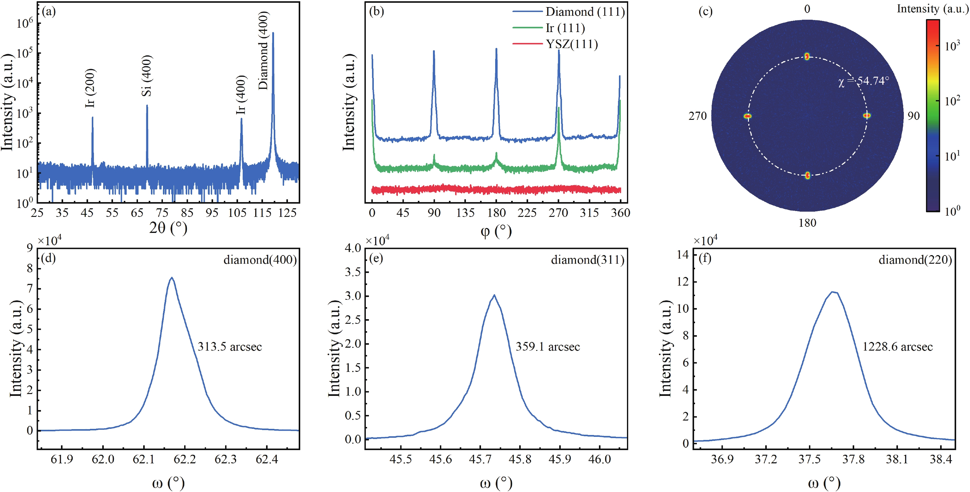
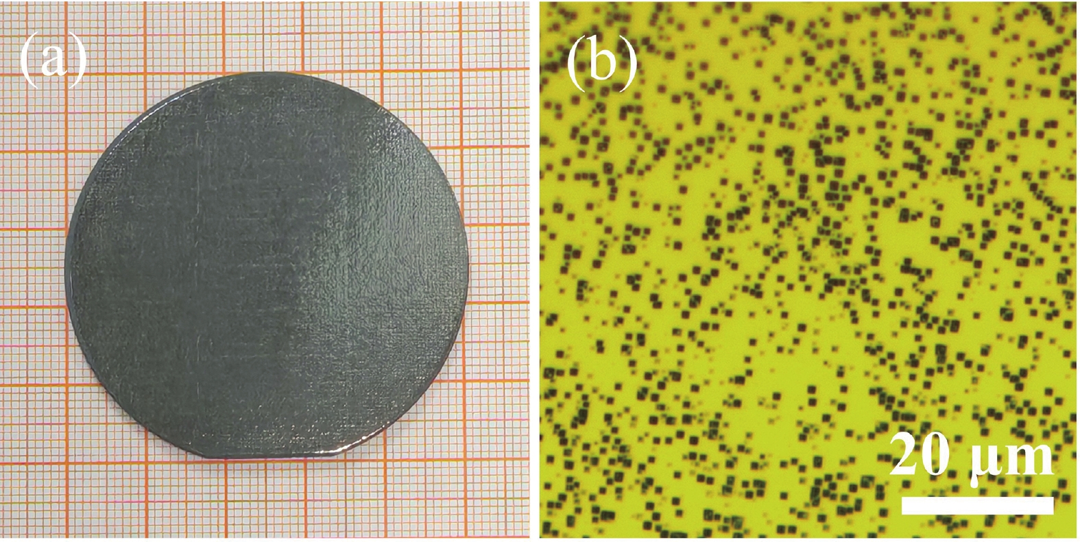
Processing math: 100%
J. Semicond. > 2024, Volume 45 > Issue 9 > 090501

SHORT COMMUNICATION

Growth of two-inch free-standing heteroepitaxial diamond on Ir/YSZ/Si (001) substrates via laser-patterned templates

Pengfei Qu1, 2, Peng Jin1, 2, , Guangdi Zhou1, 2, Zhen Wang1, 2 and Zhanguo Wang1, 2

+ Author Affiliations

 Corresponding author: Peng Jin, pengjin@semi.ac.cn

DOI: 10.1088/1674-4926/24060003

PDF

Turn off MathJax

As an ultra-wide bandgap semiconductor, diamond garners significant interest due to its exceptional physical properties[13]. These superior characteristics make diamonds highly promising for applications in power electronics[4], deep-ultraviolet detectors[5], high-energy particle detectors[6], and quantum devices based on color centers[7]. A high-quality inch-sized monocrystalline diamond wafer is fundamental for massive semiconductor device research. Nevertheless, preparing such diamond wafers constitutes one of the major technological challenges in commercializing diamond materials and devices. Over several decades of development, the heteroepitaxial growth of diamonds on Ir composite substrates, combined with bias-enhanced nucleation (BEN) process, has emerged as the most promising method for producing inch-sized monocrystalline diamonds[815]. However, achieving large-sized heteroepitaxial diamonds in practice remains challenging. The disparity in lattice parameters between hetero-substrates and diamonds leads to high threading dislocation densities, typically in the range of 107−109 cm−2 for a few hundred micrometers thickness[16]. Additionally, the complex strain control within the diamond–iridium composite system and the thermal mismatch due to differences in thermal expansion coefficients induce stress up to the GPa level in diamond thin films[17, 18]. This stress often causes cracking of the diamond epitaxial layers, hindering the growth of thick diamond wafers[19].

Significant endeavors have been dedicated to diminishing dislocation densities and releasing stress in heteroepitaxial diamonds. In 2017, Schreck et al. fabricated an around 92 mm diameter, 1.6 mm thick freestanding heteroepitaxial diamond plate on Ir/YSZ/Si (001) (with YSZ = yttria stabilized zirconia), the largest single-crystal diamond ever reported[14]. This achievement was facilitated by applying high-power conditions (915 MHz) in their microwave-plasma chemical vapor deposition (MPCVD) setup to ensure a more homogeneous growth environment. Besides, Kim et al. grew 1-inch high-quality self-supported diamonds with a thickness ranging from 500−600 μm after double-sided polishing on Ir (001)/sapphire (11ˉ20) using the microneedle method[11]. Subsequently, they accomplished 2-inch high-quality freestanding monocrystalline diamonds on A-sapphire substrates with a misoriented angle of up to 7° in a step-flow growth mode[12]. This letter presents a practical and dependable approach for growing sizable diamond single crystals. We introduce the utilization of a laser beam to create patterns on the surface of a 50 nm diamond layer grown on BEN-treated Ir/YSZ/Si (001) substrates. These laser-patterned templates effectively ease the stress within the diamond layer, thereby facilitating the growth of a robust 2-inch freestanding diamond. The resultant diamond remains intact, devoid of cracks, promising crystal quality and low dislocation density.

Fig. 1 illustrates schematically the fabrication process of the freestanding heteroepitaxial diamond grown on Ir/YSZ/Si (001) via laser-patterned templates. Firstly, a 100 nm thick YSZ epilayer and a 120 nm thick Ir epilayer were sequentially deposited on a 2-inch Si (001) single-crystal substrate using a PLD setup. Details of preparing the YSZ and Ir epilayers are described in our previous work[20, 21]. Then, BEN treatment for diamond nucleation was performed on the prepared Ir/YSZ/Si (001) substrate in a specialized apparatus (DN2106) based on microwave plasma. The bias voltage was −300 V, and the duration was 40 min. Onto the BEN-treated Ir composite substrate, a thin diamond film of around 50 nm was grown. A 355-nm ultraviolet laser with a power of 500 mW was employed to create 500 μm × 500 μm square patterns with lateral faces along <110> direction. The width treated by the laser is 20 μm. The growth of a thick diamond layer was then carried out using the MPCVD reactor under optimized growth conditions. The diamond patterns underwent an epitaxial lateral overgrowth (ELO) process to achieve a coalescence, forming a closed and continuous diamond epilayer at the first 200 μm thickness. At the latter stage of the CVD growth, nitrogen was slightly added to the ambient gas to increase the growth rate. During the cooling process, the diamond/Ir layers automatically detached from the Si substrate due to the coefficient of thermal expansion (CTE) induced thermal strain. The growth of the thick diamond lasted for 80 h, resulting in a final thickness of around 400 μm.

Fig. 1.  (Color online) Schematic diagram of fabrication procedure of heteroepitaxial diamond on Ir/YSZ/Si (001). (a) 2-inch Si (001) substrate. (b) YSZ buffer layer deposition. (c) Ir buffer layer deposition. (d) Diamond nucleation by BEN. (e) Thin diamond growth. (f) Laser patterned diamond template. (g) Thick diamond growth. (h) Diamond self-detachment.

Fig. 2 shows the X-ray diffraction (XRD) results of the heteroepitaxial diamond grown on Ir/YSZ/Si (001) for 80 h. The resultant diamond is around 400 μm thick. The XRD θ−2θ scan shown in Fig. 2(a) exhibits four prominent diffraction peaks corresponding to Ir (200) (2θ = 47.3°), Si (400) (2θ = 69.2°), Ir (400) (2θ = 106.7°), and diamond (400) (2θ = 119.3°), verifying a pure (001)-oriented alignment and an excellent crystallinity. Mutual orientations among the diamond, Ir, YSZ, and Si substrate were verified by an in-plane φ scan of the {111} diffraction peaks of each layer at χ = 54.74°. As shown in Fig. 2(b), the φ scan results of diamond and iridium layers show an exact quadruple symmetry with φ angles occurring at φ = 0°, 90°, 180°, and 270°. No diffraction peaks of the YSZ layer and silicon substrate (not shown here) were detected, probably because they exceeded the penetration depth of X-rays. It was proved that the Ir/YSZ/Si substrate has a cube-on-cube crystallographic epitaxial relationship in our previous work. Therefore, this result demonstrates the same crystallographic epitaxial relationship in the diamond/Ir/YSZ/Si system. Furthermore, the X-ray pole figure of diamond {111} diffractions from the as-grown diamond crystal is shown in Fig. 2(c). The absence of additional peaks except for four {111} diffraction peaks evidences that no twinning is found in the diamond crystal. The X-ray rocking curves (XRCs) of diamond (400), (311), and (220) diffractions are displayed in Figs. 2(d)−2(f), respectively. The full width at half maximum (FWHM) of respective XRCs are 313.5, 359.1, and 1228.6 arcsecs, respectively, confirming the good epitaxial quality of the resultant diamond.

Fig. 2.  (Color online) (a) X-ray diffractograms of θ−2θ scan of the heteroepitaxial diamond on Ir/YSZ/Si (001). (b) In-plane φ scan of diamond {111} and Ir {111} at a polar angle of χ = 54.74°. (c) X-ray pole figure of diamond {111} diffraction peaks. (d) XRCs of diamond (400), (e) diamond (311), and (f) diamond (220) diffraction peaks from the freestanding diamond.

Fig. 3(a) shows a picture of the 2-inch freestanding diamond crystal with a thickness of 400 μm. The dim color is a result of nitrogen impurities. Owing to the thermal strain and the partial attachment of the diamond to the Ir interface, the diamond/Ir layers detached from the Si substrate during the cooling process. This diamond plate was obtained without cracks and fracturing. To quantitatively evaluate dislocation density and its distribution, we subjected the diamond surface to H2/O2 plasma etching within the MPCVD setup. Under the etching conditions involving a microwave power of 3 kW, a gas pressure of 150 Torr, and a substrate temperature of 850 °C, the process was executed for 20 min. The density of these dislocation features was determined to be approximately 2.2 × 107 cm−2, a value consistent with the lowest dislocation levels observed in heteroepitaxial diamonds.

Fig. 3.  (Color online) (a) Picture of the 2-inch freestanding diamond crystal grown on Ir/YSZ/Si (001). (b) Microscope image of the as-grown diamond surface after plasma etching to reveal dislocation.

In short, 2-inch free-standing diamonds were prepared by using heteroepitaxy on composite Ir/YSZ/Si (001) substrates. To release stress, patterned templates were fabricated using laser etching after the initial growth of 50-nm-diamond. Then, the subsequent growth was completed on a patterned template. The FWHM of the diamond (400) and (311) X-ray rocking curves were 313 and 359 arcsecs, respectively. The dislocation density determined by counting etching pits was approximately 2.2 × 107 cm−2. These results evidence that the laser-patterned method can effectively release stress during the growth of large-size diamonds, offering a simpler and more cost-effective alternative to the traditional photolithography-patterned scheme.

This work is supported by the National Key Research and Development Program of China (Grant No. 2022YFB3608600), the Beijing Municipal Science and Technology Commission (Grant No. Z181100004418009) and the National Natural Science Foundation of China (Grant No. 61927806).


[1]
Wort C J H, Balmer R S. Diamond as an electronic material. Mater Today, 2008, 11, 22 doi: 10.1016/S1369-7021(07)70349-8
[2]
Isberg J, Hammersberg J, Johansson E, et al. High carrier mobility in single-crystal plasma-deposited diamond. Science, 2002, 297, 1670 doi: 10.1126/science.1074374
[3]
Inyushkin A V, Taldenkov A N, Ralchenko V G, et al. Thermal conductivity of high purity synthetic single crystal diamonds. Phys Rev B, 2018, 97, 144305 doi: 10.1103/PhysRevB.97.144305
[4]
Kwak T, Lee J, Choi U, et al. Diamond Schottky barrier diodes fabricated on sapphire-based freestanding heteroepitaxial diamond substrate. Diam Relat Mater, 2021, 114, 108335 doi: 10.1016/j.diamond.2021.108335
[5]
Feng M, Jin P, Meng X, et al. Performance of metal-semiconductor-metal structured diamond deep-ultraviolet photodetector with a large active area. J Phys D: Appl Phy, 2022, 55, 404005 doi: 10.1088/1361-6463/ac83ce
[6]
Salvadori M, Consoli F, Verona C, et al. Accurate spectra for high energy ions by advanced time-of-flight diamond-detector schemes in experiments with high energy and intensity lasers. Sci Rep, 2021, 11, 3071 doi: 10.1038/s41598-021-82655-w
[7]
Prawer S, Greentree A D. Diamond for quantum computing. Science, 2008, 320, 1601 doi: 10.1126/science.1158340
[8]
Schreck M, Asmussen J, Shikata S, et al. Large-area high-quality single crystal diamond. MRS Bull, 2014, 39, 504 doi: 10.1557/mrs.2014.96
[9]
Arnault J C, Lee K H, Delchevalrie J, et al. Epitaxial diamond on Ir/SrTiO3/Si (001): From sequential material characterizations to fabrication of lateral Schottky diodes. Diam Relat Mater, 2020, 105, 107768 doi: 10.1016/j.diamond.2020.107768
[10]
Tang Y H, Golding B. Stress engineering of high-quality single crystal diamond by heteroepitaxial lateral overgrowth. Appl Phys Lett, 2016, 108, 052101 doi: 10.1063/1.4941291
[11]
Kim S W, Kawamata Y, Takaya R, et al. Growth of high-quality one-inch free-standing heteroepitaxial (001) diamond on ( 11ˉ20) sapphire substrate. Appl Phys Lett, 2020, 117, 202102 doi: 10.1063/5.0024070
[12]
Kim S W, Takaya R, Hirano S, et al. Two-inch high-quality (001) diamond heteroepitaxial growth on sapphire ( 11ˉ20) misoriented substrate by step-flow mode. Appl Phys Express, 2021, 14, 115501 doi: 10.35848/1882-0786/ac28e7
[13]
Ichikawa K, Kurone K, Kodama H, et al. High crystalline quality heteroepitaxial diamond using grid-patterned nucleation and growth on Ir. Diam Relat Mater, 2019, 94, 92 doi: 10.1016/j.diamond.2019.01.027
[14]
Schreck M, Gsell S, Brescia R, et al. Ion bombardment induced buried lateral growth: the key mechanism for the synthesis of single crystal diamond wafers. Sci Rep, 2017, 7, 44462 doi: 10.1038/srep44462
[15]
Lebedev V, Kustermann J, Engels J, et al. Coalescence as a key process in wafer-scale diamond heteroepitaxy. J Appl Phys, 2024, 135, 145302 doi: 10.1063/5.0189631
[16]
Stehl C, Fischer M, Gsell S, et al. Efficiency of dislocation density reduction during heteroepitaxial growth of diamond for detector applications. Appl Phys Lett, 2013, 103, 151905 doi: 10.1063/1.4824330
[17]
Aida H, Ihara T, Oshima R, et al. Analysis of external surface and internal lattice curvatures of freestanding heteroepitaxial diamond grown on an Ir (001)/MgO (001) substrate. Diam Relat Mater, 2023, 136, 110026 doi: 10.1016/j.diamond.2023.110026
[18]
Kasu M, Takaya R, Kim S W. Growth of high-quality inch-diameter heteroepitaxial diamond layers on sapphire substrates in comparison to MgO substrates. Diam Relat Mater, 2022, 126, 109086 doi: 10.1016/j.diamond.2022.109086
[19]
Kimura Y, Ihara T, Ojima T, et al. Physical bending of heteroepitaxial diamond grown on an Ir/MgO substrate. Diam Relat Mater, 2023, 110055 doi: 10.1016/j.diamond.2023.110055
[20]
Qu P, Jin P, Zhou G, et al. Epitaxial growth of high-quality yttria-stabilized zirconia films with uniform thickness on silicon by the combination of PLD and RF sputtering. Surf Coat Technol, 2023, 456, 129267 doi: 10.1016/j.surfcoat.2023.129267
[21]
Zhou G, Qu P, Huo X, et al. The deposition of Ir/YSZ double-layer thin films on silicon by PLD and magnetron sputtering: Growth kinetics and the effects of oxygen. Results Phys, 2023, 47, 106357 doi: 10.1016/j.rinp.2023.106357
Fig. 1.  (Color online) Schematic diagram of fabrication procedure of heteroepitaxial diamond on Ir/YSZ/Si (001). (a) 2-inch Si (001) substrate. (b) YSZ buffer layer deposition. (c) Ir buffer layer deposition. (d) Diamond nucleation by BEN. (e) Thin diamond growth. (f) Laser patterned diamond template. (g) Thick diamond growth. (h) Diamond self-detachment.

Fig. 2.  (Color online) (a) X-ray diffractograms of θ−2θ scan of the heteroepitaxial diamond on Ir/YSZ/Si (001). (b) In-plane φ scan of diamond {111} and Ir {111} at a polar angle of χ = 54.74°. (c) X-ray pole figure of diamond {111} diffraction peaks. (d) XRCs of diamond (400), (e) diamond (311), and (f) diamond (220) diffraction peaks from the freestanding diamond.

Fig. 3.  (Color online) (a) Picture of the 2-inch freestanding diamond crystal grown on Ir/YSZ/Si (001). (b) Microscope image of the as-grown diamond surface after plasma etching to reveal dislocation.

[1]
Wort C J H, Balmer R S. Diamond as an electronic material. Mater Today, 2008, 11, 22 doi: 10.1016/S1369-7021(07)70349-8
[2]
Isberg J, Hammersberg J, Johansson E, et al. High carrier mobility in single-crystal plasma-deposited diamond. Science, 2002, 297, 1670 doi: 10.1126/science.1074374
[3]
Inyushkin A V, Taldenkov A N, Ralchenko V G, et al. Thermal conductivity of high purity synthetic single crystal diamonds. Phys Rev B, 2018, 97, 144305 doi: 10.1103/PhysRevB.97.144305
[4]
Kwak T, Lee J, Choi U, et al. Diamond Schottky barrier diodes fabricated on sapphire-based freestanding heteroepitaxial diamond substrate. Diam Relat Mater, 2021, 114, 108335 doi: 10.1016/j.diamond.2021.108335
[5]
Feng M, Jin P, Meng X, et al. Performance of metal-semiconductor-metal structured diamond deep-ultraviolet photodetector with a large active area. J Phys D: Appl Phy, 2022, 55, 404005 doi: 10.1088/1361-6463/ac83ce
[6]
Salvadori M, Consoli F, Verona C, et al. Accurate spectra for high energy ions by advanced time-of-flight diamond-detector schemes in experiments with high energy and intensity lasers. Sci Rep, 2021, 11, 3071 doi: 10.1038/s41598-021-82655-w
[7]
Prawer S, Greentree A D. Diamond for quantum computing. Science, 2008, 320, 1601 doi: 10.1126/science.1158340
[8]
Schreck M, Asmussen J, Shikata S, et al. Large-area high-quality single crystal diamond. MRS Bull, 2014, 39, 504 doi: 10.1557/mrs.2014.96
[9]
Arnault J C, Lee K H, Delchevalrie J, et al. Epitaxial diamond on Ir/SrTiO3/Si (001): From sequential material characterizations to fabrication of lateral Schottky diodes. Diam Relat Mater, 2020, 105, 107768 doi: 10.1016/j.diamond.2020.107768
[10]
Tang Y H, Golding B. Stress engineering of high-quality single crystal diamond by heteroepitaxial lateral overgrowth. Appl Phys Lett, 2016, 108, 052101 doi: 10.1063/1.4941291
[11]
Kim S W, Kawamata Y, Takaya R, et al. Growth of high-quality one-inch free-standing heteroepitaxial (001) diamond on ( 11ˉ20) sapphire substrate. Appl Phys Lett, 2020, 117, 202102 doi: 10.1063/5.0024070
[12]
Kim S W, Takaya R, Hirano S, et al. Two-inch high-quality (001) diamond heteroepitaxial growth on sapphire ( 11ˉ20) misoriented substrate by step-flow mode. Appl Phys Express, 2021, 14, 115501 doi: 10.35848/1882-0786/ac28e7
[13]
Ichikawa K, Kurone K, Kodama H, et al. High crystalline quality heteroepitaxial diamond using grid-patterned nucleation and growth on Ir. Diam Relat Mater, 2019, 94, 92 doi: 10.1016/j.diamond.2019.01.027
[14]
Schreck M, Gsell S, Brescia R, et al. Ion bombardment induced buried lateral growth: the key mechanism for the synthesis of single crystal diamond wafers. Sci Rep, 2017, 7, 44462 doi: 10.1038/srep44462
[15]
Lebedev V, Kustermann J, Engels J, et al. Coalescence as a key process in wafer-scale diamond heteroepitaxy. J Appl Phys, 2024, 135, 145302 doi: 10.1063/5.0189631
[16]
Stehl C, Fischer M, Gsell S, et al. Efficiency of dislocation density reduction during heteroepitaxial growth of diamond for detector applications. Appl Phys Lett, 2013, 103, 151905 doi: 10.1063/1.4824330
[17]
Aida H, Ihara T, Oshima R, et al. Analysis of external surface and internal lattice curvatures of freestanding heteroepitaxial diamond grown on an Ir (001)/MgO (001) substrate. Diam Relat Mater, 2023, 136, 110026 doi: 10.1016/j.diamond.2023.110026
[18]
Kasu M, Takaya R, Kim S W. Growth of high-quality inch-diameter heteroepitaxial diamond layers on sapphire substrates in comparison to MgO substrates. Diam Relat Mater, 2022, 126, 109086 doi: 10.1016/j.diamond.2022.109086
[19]
Kimura Y, Ihara T, Ojima T, et al. Physical bending of heteroepitaxial diamond grown on an Ir/MgO substrate. Diam Relat Mater, 2023, 110055 doi: 10.1016/j.diamond.2023.110055
[20]
Qu P, Jin P, Zhou G, et al. Epitaxial growth of high-quality yttria-stabilized zirconia films with uniform thickness on silicon by the combination of PLD and RF sputtering. Surf Coat Technol, 2023, 456, 129267 doi: 10.1016/j.surfcoat.2023.129267
[21]
Zhou G, Qu P, Huo X, et al. The deposition of Ir/YSZ double-layer thin films on silicon by PLD and magnetron sputtering: Growth kinetics and the effects of oxygen. Results Phys, 2023, 47, 106357 doi: 10.1016/j.rinp.2023.106357
1

Perovskite plasmonic lasers capable of mode modulation

Jingbi You

Journal of Semiconductors, 2019, 40(7): 070203. doi: 10.1088/1674-4926/40/7/070203

2

Colloidal synthesis and characterization of Cu2ZnSnS4 nanoplates

S. Ananthakumar, J. Ram Kumar, S. Moorthy Babu

Journal of Semiconductors, 2017, 38(3): 033007. doi: 10.1088/1674-4926/38/3/033007

3

Substrate temperature dependent studies on properties of chemical spray pyrolysis deposited CdS thin films for solar cell applications

Kiran Diwate, Amit Pawbake, Sachin Rondiya, Rupali Kulkarni, Ravi Waykar, et al.

Journal of Semiconductors, 2017, 38(2): 023001. doi: 10.1088/1674-4926/38/2/023001

4

Improved interfacial properties of GaAs MOS capacitor with NH3-plasma-treated ZnON as interfacial passivation layer

Jingkang Gong, Jingping Xu, Lu Liu, Hanhan Lu, Xiaoyu Liu, et al.

Journal of Semiconductors, 2017, 38(9): 094004. doi: 10.1088/1674-4926/38/9/094004

5

Catalyst-free growth of ZnO nanowires on various-oriented sapphire substrates by pulsed-laser deposition

Tetsuya Shimogaki, Masahiro Takahashi, Masaaki Yamasaki, Taichi Fukuda, Mitsuhiro Higashihata, et al.

Journal of Semiconductors, 2016, 37(2): 023001. doi: 10.1088/1674-4926/37/2/023001

6

Unstrained InAlN/GaN heterostructures grown on sapphire substrates by MOCVD

Bo Liu, Jiayun Yin, Yuanjie Lü, Shaobo Dun, Xiongwen Zhang, et al.

Journal of Semiconductors, 2014, 35(11): 113005. doi: 10.1088/1674-4926/35/11/113005

7

MOCVD epitaxy of InAlN on different templates

Yun Lijun, Wei Tongbo, Yan Jianchang, Liu Zhe, Wang Junxi, et al.

Journal of Semiconductors, 2011, 32(9): 093001. doi: 10.1088/1674-4926/32/9/093001

8

Conductivity modulation enhanced lateral IGBT with SiO2 shielded layer anode by SIMOX technology on SOI substrate

Chen Wensuo, Zhang Bo, Li Zhaoji, Fang Jian, Guan Xu, et al.

Journal of Semiconductors, 2010, 31(6): 064004. doi: 10.1088/1674-4926/31/6/064004

9

Fast patterning and dry-etch of SiNx for high resolution nanoimprint templates

Shu Zhen, Wan Jing, Lu Bingrui, Xie Shenqi, Chen Yifang, et al.

Journal of Semiconductors, 2009, 30(6): 066001. doi: 10.1088/1674-4926/30/6/066001

10

High quality AlGaN grown on a high temperature AlN template by MOCVD

Yan Jianchang, Wang Junxi, Liu Naixin, Liu Zhe, Ruan Jun, et al.

Journal of Semiconductors, 2009, 30(10): 103001. doi: 10.1088/1674-4926/30/10/103001

11

Heteroepitaxial Growth of 3C-SiC Films on Maskless Patterned Silicon Substrates

Zhao Yongmei, Sun Guosheng, Ning Jin, Liu Xingfang, Zhao Wanshun, et al.

Journal of Semiconductors, 2008, 29(7): 1254-1257.

12

Growth of p-GaN on High-Temperature AlN Templates

Liu Ting, Zou Zeya, Wang Zhen, Zhao Hong, Zhao Wenbo, et al.

Journal of Semiconductors, 2008, 29(1): 128-132.

13

Growth of Free-Standing AlN Nanocrystals on Nanorod ZnO Template

Hu Weiguo, Wei Hongyuan, Jiao Chunmei, Kang Tingting, Zhang Riqing, et al.

Chinese Journal of Semiconductors , 2007, 28(10): 1508-1512.

14

Dislocation Reduction in GaN on Sapphire by Epitaxial Lateral Overgrowth

Chen Jun, Wang Jianfeng, Wang Hui, Zhao Degang, Zhu Jianjun, et al.

Chinese Journal of Semiconductors , 2006, 27(3): 419-424.

15

Lateral Oxidation in Vertical Cavity Surface Emitting Lasers

Liu Wenli, Hao Yongqin, Wang Yuxia, Jiang Xiaoguang, Feng Yuan, et al.

Chinese Journal of Semiconductors , 2006, 27(8): 1351-1354.

16

A New Clustering-Based Partitioning Method for VLSI Mixed-Mode Placement

Lü Yongqiang, Hong Xianlong, Yang Changqi, Zhou Qiang, and Cai Yici, et al.

Chinese Journal of Semiconductors , 2005, 26(1): 22-28.

17

Simulation of a Monolithic Integrated CMOS Preamplifier for Neural Recordings

Sui Xiaohong, Liu Jinbin, Gu Ming, Pei Weihua, Chen Hongda, et al.

Chinese Journal of Semiconductors , 2005, 26(12): 2275-2280.

18

Material Growth and Device Fabrication of GaN-Based Blue-Violet Laser Diodes

Yang Hui, Chen Lianghui, Zhang Shuming, Chong Ming, Zhu Jianjun, et al.

Chinese Journal of Semiconductors , 2005, 26(2): 414-417.

19

1.55μm Laser Diode Monolithically Integrated with Spot-Size Converter Using Conventional Process

Hou Lianping, Wang Wei, and Zhu Hongliang

Chinese Journal of Semiconductors , 2005, 26(3): 443-447.

20

Growth and Characterisation of InAsSb Ternary Layers on (101) GaSb Substrates by LP-MOCVD

Li Xiaoting, Wang Tao, Wang Jingwei, Wang Yiding, Yin Jingzhi, et al.

Chinese Journal of Semiconductors , 2005, 26(12): 2298-2302.

1. Kajiyama, K., Haruyama, M., Hatano, Y. et al. Heteroepitaxial (111) Diamond Quantum Sensors with Preferentially Aligned Nitrogen-Vacancy Centers for an Electric Vehicle Battery Monitor. Advanced Quantum Technologies, 2025, 8(4): 2400400. doi:10.1002/qute.202400400
2. Zhang, X., Xu, M., Ng, Z.K. et al. Diamond: Recent Progress in Synthesis and Its Potential in Electronics. Chemistry of Materials, 2025. doi:10.1021/acs.chemmater.5c00248
  • Search

    Advanced Search >>

    GET CITATION

    Pengfei Qu, Peng Jin, Guangdi Zhou, Zhen Wang, Zhanguo Wang. Growth of two-inch free-standing heteroepitaxial diamond on Ir/YSZ/Si (001) substrates via laser-patterned templates[J]. Journal of Semiconductors, 2024, 45(9): 090501. doi: 10.1088/1674-4926/24060003
    P F Qu, P Jin, G D Zhou, Z Wang, and Z G Wang, Growth of two-inch free-standing heteroepitaxial diamond on Ir/YSZ/Si (001) substrates via laser-patterned templates[J]. J. Semicond., 2024, 45(9), 090501 doi: 10.1088/1674-4926/24060003
    shu

    Export: BibTex EndNote

    Article Metrics

    Article views: 1202 Times PDF downloads: 139 Times Cited by: 2 Times

    History

    Received: 03 June 2024 Revised: 01 July 2024 Online: Accepted Manuscript: 04 July 2024Uncorrected proof: 04 July 2024Published: 15 September 2024

    Catalog

      Email This Article

      User name:
      Email:*请输入正确邮箱
      Code:*验证码错误
      Pengfei Qu, Peng Jin, Guangdi Zhou, Zhen Wang, Zhanguo Wang. Growth of two-inch free-standing heteroepitaxial diamond on Ir/YSZ/Si (001) substrates via laser-patterned templates[J]. Journal of Semiconductors, 2024, 45(9): 090501. doi: 10.1088/1674-4926/24060003 ****P F Qu, P Jin, G D Zhou, Z Wang, and Z G Wang, Growth of two-inch free-standing heteroepitaxial diamond on Ir/YSZ/Si (001) substrates via laser-patterned templates[J]. J. Semicond., 2024, 45(9), 090501 doi: 10.1088/1674-4926/24060003
      Citation:
      Pengfei Qu, Peng Jin, Guangdi Zhou, Zhen Wang, Zhanguo Wang. Growth of two-inch free-standing heteroepitaxial diamond on Ir/YSZ/Si (001) substrates via laser-patterned templates[J]. Journal of Semiconductors, 2024, 45(9): 090501. doi: 10.1088/1674-4926/24060003 ****
      P F Qu, P Jin, G D Zhou, Z Wang, and Z G Wang, Growth of two-inch free-standing heteroepitaxial diamond on Ir/YSZ/Si (001) substrates via laser-patterned templates[J]. J. Semicond., 2024, 45(9), 090501 doi: 10.1088/1674-4926/24060003

      Growth of two-inch free-standing heteroepitaxial diamond on Ir/YSZ/Si (001) substrates via laser-patterned templates

      DOI: 10.1088/1674-4926/24060003
      More Information
      • Pengfei Qu got his Bachelor degree in 2019 from Jilin University. He is now a PhD student at Institute of Semiconductors, CAS under the supervision of Prof. Peng Jin. His current research focuses on the heteroepitaxial growth of monocrystalline diamonds
      • Peng Jin got his BS and PhD from Nankai University in 1996 and 2001, respectively. He did postdoctoral research at Institute of Semiconductors, CAS. In 2003, he joined Institute of Semiconductors, CAS as an associate professor. In 2009, he was promoted to be a professor. In 2015, he became a professor of UCAS. The current research focuses on semiconductor diamond materials and devices, low dimensional semiconductor materials and devices, scientific instruments, etc
      • Corresponding author: pengjin@semi.ac.cn
      • Received Date: 2024-06-03
      • Revised Date: 2024-07-01
      • Available Online: 2024-07-04

      Catalog

        /

        DownLoad:  Full-Size Img  PowerPoint
        Return
        Return