Just Accepted

Just Accepted manuscripts are peer-reviewed and accepted for publication. They are posted online prior to technical editing formatting for publication and author proofing.
High-speed electro-absorption modulated laser
Zhenyao Li, Chen Lyu, Xuliang Zhou, Mengqi Wang, Haotian Qiu, Yejin Zhang, Hongyan Yu, Jiaoqing Pan
, Available online  

doi: 10.1088/1674-4926/25030015

Currently, the global 5G network, cloud computing, and data center industries are experiencing rapid development. The continuous growth of data center traffic has driven the vigorous progress in high-speed optical transceivers for optical interconnection within data centers. The electro-absorption modulated laser (EML), which is widely used in optical fiber communications, data centers, and high-speed data transmission systems, represents a high-performance photoelectric conversion device. Compared to traditional directly modulated lasers (DMLs), EMLs demonstrate lower frequency chirp and higher modulation bandwidth, enabling support for higher data rates and longer transmission distances. This article introduces the composition, working principles, manufacturing processes, and applications of EMLs. It reviews the progress on advanced indium phosphide (InP)-based EML devices from research institutions worldwide, while summarizing and comparing data transmission rates and key technical approaches across various studies.

Currently, the global 5G network, cloud computing, and data center industries are experiencing rapid development. The continuous growth of data center traffic has driven the vigorous progress in high-speed optical transceivers for optical interconnection within data centers. The electro-absorption modulated laser (EML), which is widely used in optical fiber communications, data centers, and high-speed data transmission systems, represents a high-performance photoelectric conversion device. Compared to traditional directly modulated lasers (DMLs), EMLs demonstrate lower frequency chirp and higher modulation bandwidth, enabling support for higher data rates and longer transmission distances. This article introduces the composition, working principles, manufacturing processes, and applications of EMLs. It reviews the progress on advanced indium phosphide (InP)-based EML devices from research institutions worldwide, while summarizing and comparing data transmission rates and key technical approaches across various studies.
Effect of nitrogen incorporation and surface passivation on photoluminescence properties of InAs-based nanowires
Ratmir Ustimenko, Danila Karaulov, Maxim Vinnichenko, Ilya Norvatov, Andrey Kaveev, Vladimir Fedorov, Ivan Mukhin, Dmitry Firsov
, Available online  

doi: 10.1088/1674-4926/25030041

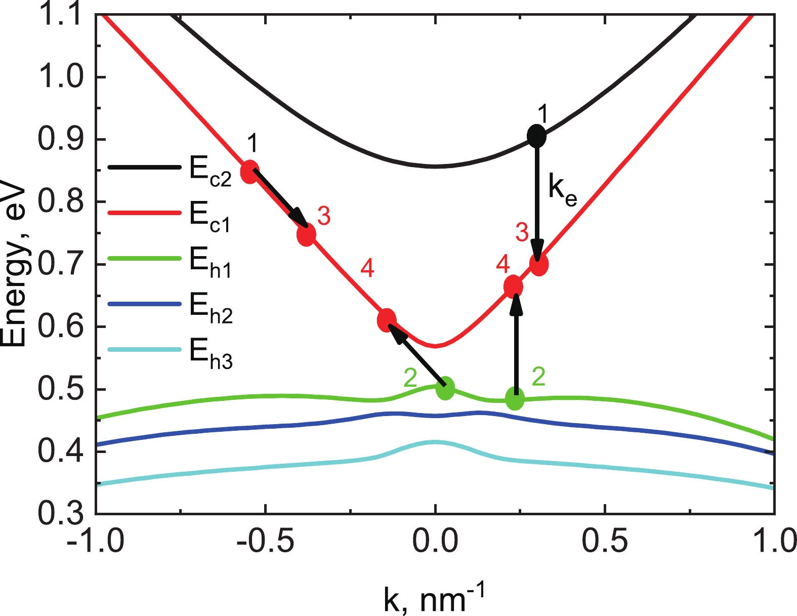
InAsN nanowires on InAs stems were obtained using plasma-assisted molecular beam epitaxy on a SiOx/Si (111) substrate. Also, heterostructured InAs/InAsN and InAsN/InP nanowires were grown in the core/shell geometry. In the low-temperature photoluminescence spectra of the grown structures, spectral features are observed that correspond to the polytypic structure of nanowires with a predominance of the wurtzite phase and parasitic islands of the sphalerite phase. It was shown that the interband photoluminescence spectral features of InAsN nanowires experience a red shift relative to the pristine InAs nanowires. The incorporation of nitrogen reduces the bandgap by splitting the conduction band into two subbands. The position of the spectral features in the photoluminescence spectra confirms the formation of a nitride solid solution with a polytypic hexagonal structure, having a concentration of nitrogen atoms of up to 0.7%. Additional passivation of the nanowire surface with InP leads to a decrease in the intensity of nonradiative recombination and an improvement in the photoluminescent response of the nanowires, which makes it possible to detect photoluminescence emission at room temperature. Thus, by changing the composition and morphology of nanowires, it is possible to control their electronic structure, which allows varying the operating range of detectors and mid-IR radiation sources based on them.

InAsN nanowires on InAs stems were obtained using plasma-assisted molecular beam epitaxy on a SiOx/Si (111) substrate. Also, heterostructured InAs/InAsN and InAsN/InP nanowires were grown in the core/shell geometry. In the low-temperature photoluminescence spectra of the grown structures, spectral features are observed that correspond to the polytypic structure of nanowires with a predominance of the wurtzite phase and parasitic islands of the sphalerite phase. It was shown that the interband photoluminescence spectral features of InAsN nanowires experience a red shift relative to the pristine InAs nanowires. The incorporation of nitrogen reduces the bandgap by splitting the conduction band into two subbands. The position of the spectral features in the photoluminescence spectra confirms the formation of a nitride solid solution with a polytypic hexagonal structure, having a concentration of nitrogen atoms of up to 0.7%. Additional passivation of the nanowire surface with InP leads to a decrease in the intensity of nonradiative recombination and an improvement in the photoluminescent response of the nanowires, which makes it possible to detect photoluminescence emission at room temperature. Thus, by changing the composition and morphology of nanowires, it is possible to control their electronic structure, which allows varying the operating range of detectors and mid-IR radiation sources based on them.
Breathable and skin-conformal electronic skin with dual-modality synchronous perception of pressure and temperature
Hao Zhu, Zhelin Jin, Tie Li, Guanggui Cheng, Jianning Ding
, Available online  

doi: 10.1088/1674-4926/25020031

The random nanofiber distribution in traditional electrospun membranes restricts the pressure sensing sensitivity and measurement range of electronic skin. Moreover, current multimodal sensing suffers from issues like overlapping signal outputs and slow response. Herein, a novel electrospinning method is proposed to prepare double-coupled microstructured nanofibrous membranes. Through the effect of high voltage electrostatic field in the electrospinning, the positively charged nanofibers are preferentially attached to the negatively charged foam surface, forming the ordered two-dimensional honeycomb porous nanofibrous membrane with three-dimensional spinous microstructure. Compared with the conventional random porous nanofibrous membrane, the bionic two-dimensional honeycomb and three-dimensional spinous dual-coupled microstructures in the ordered porous nanofibrous membrane endows the electronic skin with significantly improved mechanical properties (maximum tensile strain increased by 77% and fatigue resistance increased by 35%), air permeability (water vapor transmission rate increased by 16%) and sensing properties (pressure sensitivity increased by 276% and detection range increased by 137%). Furthermore, the electronic skin was constructed by means of a conformal composite ionic liquid functionalized nanofibrous membrane, and the real-time and interference-free dual-signal monitoring of pressure and temperature (maximum temperature coefficient of resistance: −0.918 °C−1) was realized.

The random nanofiber distribution in traditional electrospun membranes restricts the pressure sensing sensitivity and measurement range of electronic skin. Moreover, current multimodal sensing suffers from issues like overlapping signal outputs and slow response. Herein, a novel electrospinning method is proposed to prepare double-coupled microstructured nanofibrous membranes. Through the effect of high voltage electrostatic field in the electrospinning, the positively charged nanofibers are preferentially attached to the negatively charged foam surface, forming the ordered two-dimensional honeycomb porous nanofibrous membrane with three-dimensional spinous microstructure. Compared with the conventional random porous nanofibrous membrane, the bionic two-dimensional honeycomb and three-dimensional spinous dual-coupled microstructures in the ordered porous nanofibrous membrane endows the electronic skin with significantly improved mechanical properties (maximum tensile strain increased by 77% and fatigue resistance increased by 35%), air permeability (water vapor transmission rate increased by 16%) and sensing properties (pressure sensitivity increased by 276% and detection range increased by 137%). Furthermore, the electronic skin was constructed by means of a conformal composite ionic liquid functionalized nanofibrous membrane, and the real-time and interference-free dual-signal monitoring of pressure and temperature (maximum temperature coefficient of resistance: −0.918 °C−1) was realized.
Sintering and electrical characteristics of In2O3-based targets doped with multiple components for solar cells
Jianzhong Liao, Fangzhou Wu, Jiwen Xu, Guisheng Zhu, Fei Shang, Huarui Xu
, Available online  

doi: 10.1088/1674-4926/24090038

To address the escalating demand for high-mobility transparent and conductive oxide (TCO) films in heterojunction solar cells, multiple components doped In2O3 targets were proposed. The In2O3 targets incorporating 1 wt.% CeO2, Ta2O5 and TiO2 were sintered under different sintering temperatures and times. All the targets show the cubic bixbyite phase of In2O3. The microstructure illustrates densely packed fine grains and uniform elemental distribution. Notably, increasing the sintering temperature and holding time contributes to effective pore elimination within the targets. A relative density of greater than 99.5% is obtained for the targets sintered at 1500 °C for 4 and 6 h, and the corresponding optimum resistivity decreases from 1.068×10³ Ω·cm to 9.73×10⁻⁴ Ω·cm. These results provide the experimental basis of fabricating In2O3-based targets for depositing high mobility TCO films by magnetron sputtering.

To address the escalating demand for high-mobility transparent and conductive oxide (TCO) films in heterojunction solar cells, multiple components doped In2O3 targets were proposed. The In2O3 targets incorporating 1 wt.% CeO2, Ta2O5 and TiO2 were sintered under different sintering temperatures and times. All the targets show the cubic bixbyite phase of In2O3. The microstructure illustrates densely packed fine grains and uniform elemental distribution. Notably, increasing the sintering temperature and holding time contributes to effective pore elimination within the targets. A relative density of greater than 99.5% is obtained for the targets sintered at 1500 °C for 4 and 6 h, and the corresponding optimum resistivity decreases from 1.068×10³ Ω·cm to 9.73×10⁻⁴ Ω·cm. These results provide the experimental basis of fabricating In2O3-based targets for depositing high mobility TCO films by magnetron sputtering.
Fabrication, TCAD and compact model verification of TIPS-pentacene organic thin film transistor
Shubham Dadhich, Vivek Upadhyaya, Garima Mathur
, Available online  

doi: 10.1088/1674-4926/24090029

As organic thin film transistors (OTFTs) are set to play a crucial role in flexible and cost-effective electronic applications, this paper investigates a high-mobility 6,13-bis(triisopropylsilylethynyl) Pentacene (TIPS-Pentacene) OTFT for use in flexible electronics. The development of such high-mobility devices necessitates precise device modeling to support technology optimisation and circuit design. The details of numerical simulation technique is discussed, in which, the electrical behavior of the device is well captured by fine tuning basic semiconductor equations. This technology computer-aided design (TCAD) has been validated with eprimental data. In addition, we have discussed about compact model fitting of the devices as well as parameter extraction procedure employed. This includes verification of ATLAS FEM based results against experimental data gained from fabricated OTFT devices. Simulations for p-type TFT-based inverter are also performed to assess the performance of compact model in simple circuit simulation.

As organic thin film transistors (OTFTs) are set to play a crucial role in flexible and cost-effective electronic applications, this paper investigates a high-mobility 6,13-bis(triisopropylsilylethynyl) Pentacene (TIPS-Pentacene) OTFT for use in flexible electronics. The development of such high-mobility devices necessitates precise device modeling to support technology optimisation and circuit design. The details of numerical simulation technique is discussed, in which, the electrical behavior of the device is well captured by fine tuning basic semiconductor equations. This technology computer-aided design (TCAD) has been validated with eprimental data. In addition, we have discussed about compact model fitting of the devices as well as parameter extraction procedure employed. This includes verification of ATLAS FEM based results against experimental data gained from fabricated OTFT devices. Simulations for p-type TFT-based inverter are also performed to assess the performance of compact model in simple circuit simulation.
Research on optical soliton characteristics GaSb-based ~2 μm wavelength two-section integrated optical chip
Wenjun Yu, Zhongliang Qiao, Xiang Li, Jia Xu Brian Sia, Dengqun Weng, Xiaohu Hou, Zaijin Li, Lin Li, Hao Chen, Zhibin Zhao, Yi Qu, Chongyang Liu, Hong Wang, Yu Zhang, Zhichuan Niu
, Available online  

doi: 10.1088/1674-4926/25030011

The optical soliton characteristics of GaSb-based ~2 μm wavelength integrated optical chips have broad application prospects in optoelectronic fields such as optical communications, infrared countermeasures, and gas environment monitoring. In the research of two-section integrated optical chips, more attention is paid to their passive mode-locked characteristics. The ability of its structure to generate stable soliton transmission has not yet been studied, which will limit its further application in high-performance near-mid infrared optoelectronic technology. In this paper, we design and prepare a GaSb-based ~2 μm wavelength two-section integrated semiconductor laser chip structure, and test and analyze its related properties of soliton, including power−injection current−voltage (PIV), temperature and mode-locked characteristics. Experimental results show that the chip can achieve stable mode-locked operation at nearly ~2 μm wavelength and present the working characteristics of near optical soliton states and multi-peak optical soliton states. By comparing and analyzing the measured optical pulse sequence curve with the numerical fitting based on the pure fourth order soliton approximation solution, it is confirmed that the two-section integrated optical chip structure can generate stable transmission of multi-peak optical soliton. This provides a research direction for developing near-mid infrared mode-locked integrated optical chips with high-performance property of optical soliton.

The optical soliton characteristics of GaSb-based ~2 μm wavelength integrated optical chips have broad application prospects in optoelectronic fields such as optical communications, infrared countermeasures, and gas environment monitoring. In the research of two-section integrated optical chips, more attention is paid to their passive mode-locked characteristics. The ability of its structure to generate stable soliton transmission has not yet been studied, which will limit its further application in high-performance near-mid infrared optoelectronic technology. In this paper, we design and prepare a GaSb-based ~2 μm wavelength two-section integrated semiconductor laser chip structure, and test and analyze its related properties of soliton, including power−injection current−voltage (PIV), temperature and mode-locked characteristics. Experimental results show that the chip can achieve stable mode-locked operation at nearly ~2 μm wavelength and present the working characteristics of near optical soliton states and multi-peak optical soliton states. By comparing and analyzing the measured optical pulse sequence curve with the numerical fitting based on the pure fourth order soliton approximation solution, it is confirmed that the two-section integrated optical chip structure can generate stable transmission of multi-peak optical soliton. This provides a research direction for developing near-mid infrared mode-locked integrated optical chips with high-performance property of optical soliton.
Machine learning facilitates the development of interconnecting layers for perovskite/silicon heterojunction tandem solar cells with proof-of-concept efficiency > 38%
Xuejiao Wang, Guanlan Chen, Ying Liu, Guangyi Wang, Wei Han, Jin Wang, Pengfei Liu, Jilei Wang, Shaojuan Bao, Bo Yu, Xinliang Chen, Shengzhi Xu, Ying Zhao, Xiaodan Zhang
, Available online  

doi: 10.1088/1674-4926/25050011

As the development of single-junction solar cells reaches a bottleneck, tandem solar cells have emerged as a critical pathway to further enhance power conversion efficiency. Among them, monolithic perovskite/silicon heterojunction tandem solar cells are currently the fastest-growing technology, achieving the highest efficiencies at relatively low costs. The interconnecting layer, which connects the two sub-cells, plays a crucial role in tandem cell performance. It collects electrons and holes from the respective sub-cells and facilitates recombination and tunneling at the interface. Therefore, the properties of the interconnecting layer are pivotal to the overall device performance. In this work, we applied statistical analysis and machine learning algorithms to systematically analyze the interconnecting layer. A comprehensive dataset on interconnecting layer parameters was established, and predictive modeling was performed using Lasso linear regression, random forest, and multilayer perceptron (a type of neural network). The analysis revealed key feature importance for experimental parameters, providing valuable insights into the application of interconnecting layers in perovskite/silicon heterojunction tandem solar cells. The final optimized interconnecting layer can achieve a proof-of-concept efficiency of 38.17%, providing guidance and direction for the development of monolithic perovskite/silicon tandem solar cells.

As the development of single-junction solar cells reaches a bottleneck, tandem solar cells have emerged as a critical pathway to further enhance power conversion efficiency. Among them, monolithic perovskite/silicon heterojunction tandem solar cells are currently the fastest-growing technology, achieving the highest efficiencies at relatively low costs. The interconnecting layer, which connects the two sub-cells, plays a crucial role in tandem cell performance. It collects electrons and holes from the respective sub-cells and facilitates recombination and tunneling at the interface. Therefore, the properties of the interconnecting layer are pivotal to the overall device performance. In this work, we applied statistical analysis and machine learning algorithms to systematically analyze the interconnecting layer. A comprehensive dataset on interconnecting layer parameters was established, and predictive modeling was performed using Lasso linear regression, random forest, and multilayer perceptron (a type of neural network). The analysis revealed key feature importance for experimental parameters, providing valuable insights into the application of interconnecting layers in perovskite/silicon heterojunction tandem solar cells. The final optimized interconnecting layer can achieve a proof-of-concept efficiency of 38.17%, providing guidance and direction for the development of monolithic perovskite/silicon tandem solar cells.
Study of a novel SiC-based light initiated multi-gate semiconductor switch
Chongbiao Luan, Jianqiang Yuan, Hongwei Liu, Longfei Xiao, Huiru Sha, Le Xu, Yang He, Lingyun Wang, Hongtao Li, Yupeng Huang
, Available online  

doi: 10.1088/1674-4926/25020033

To optimize turn on velocity of the SiC LIMS, we proposed a new structure for the LIMS that incorporates an optimized n+ layer and a multi-light triggered electrode design for the anode. The chip size is 5.5 mm × 5.5 mm in dimension. The experiment results indicate that the saturation laser energy required to trigger the prepared SiC LIMS has been decreased from 1.8 mJ to 40 μJ, with the forward blocking voltage of the prepared SiC LIMSs capable of withstanding over 7000 V. The leakage current is about 0.3 μA at room temperature, and the output current density achieves 4.25 kA/cm2 (with di/dt larger than 20 kA/μs).

To optimize turn on velocity of the SiC LIMS, we proposed a new structure for the LIMS that incorporates an optimized n+ layer and a multi-light triggered electrode design for the anode. The chip size is 5.5 mm × 5.5 mm in dimension. The experiment results indicate that the saturation laser energy required to trigger the prepared SiC LIMS has been decreased from 1.8 mJ to 40 μJ, with the forward blocking voltage of the prepared SiC LIMSs capable of withstanding over 7000 V. The leakage current is about 0.3 μA at room temperature, and the output current density achieves 4.25 kA/cm2 (with di/dt larger than 20 kA/μs).