


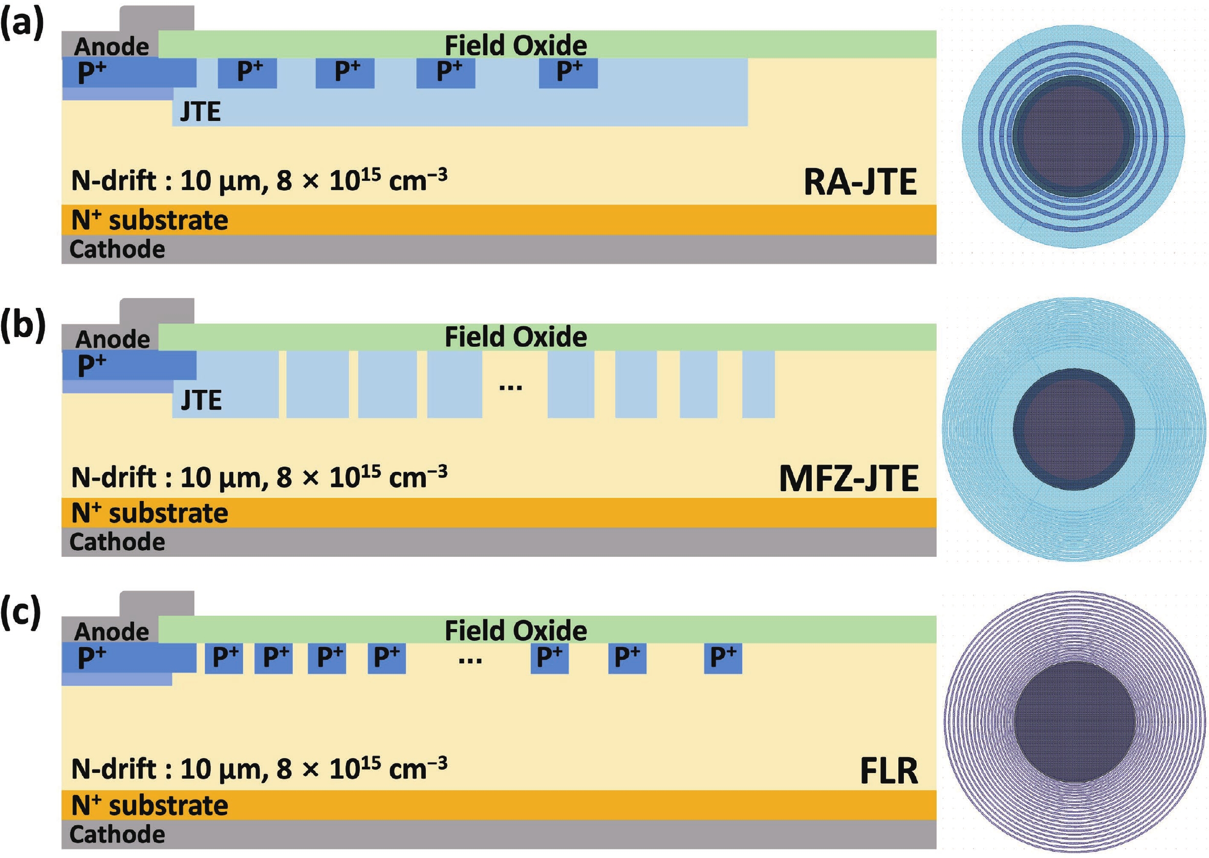
Fig. 1.
(Color online) Schematic cross-section and layouts of 1.2 kV BV-TEG consisting of (a) RA-JTE, (b) MFZ-JTE, and (c) FLR.
ARTICLES
Sangyeob Kim1, Jeongtae Kim2, 4, Dong-Seok Kim2, Hyuncheol Bae3, Min-Woo Ha5 and Ogyun Seok1,
Corresponding author: Ogyun Seok, ogseok@pusan.ac.kr
Abstract: This work presents a systematic analysis of proton-induced total ionizing dose (TID) effects in 1.2 kV silicon carbide (SiC) power devices with various edge termination structures. Three edge terminations including ring-assisted junction termination extension (RA-JTE), multiple floating zone JTE (MFZ-JTE), and field limiting rings (FLR) were fabricated and irradiated with 45 MeV protons at fluences ranging from 1 × 10¹² to 1 × 1014 cm−2. Experimental results, supported by TCAD simulations, show that the RA-JTE structure maintained stable breakdown performance with less than 1% variation due to its effective electric field redistribution by multiple P+ rings. In contrast, MFZ-JTE and FLR exhibit breakdown voltage shifts of 6.1% and 15.2%, respectively, under the highest fluence. These results demonstrate the superior radiation tolerance of the RA-JTE structure under TID conditions and provide practical design guidance for radiation-hardened SiC power devices in space and other high-radiation environments.
Keywords: SiC, proton irradiation, edge termination, radiation hardness, TID effects
| [1] |
Fard M T, He J B, Huang H, et al. Aircraft distributed electric propulsion technologies: A review. IEEE Trans Transp Electrif, 2022, 8(4): 4067 doi: 10.1109/TTE.2022.3197332
|
| [2] |
Felgemacher C, Araújo S V, Zacharias P, et al. Cosmic radiation ruggedness of Si and SiC power semiconductors. 2016 28th International Symposium on Power Semiconductor Devices and ICs (ISPSD), 2016: 51 doi: 10.1109/ISPSD.2016.7520775
|
| [3] |
Wang D, Hemming S, Yang Y H, et al. Multilevel inverters for electric aircraft applications: Current status and future trends. IEEE Trans Transp Electrif, 2024, 10(2): 3258 doi: 10.1109/TTE.2023.3296284
|
| [4] |
Dobynde M, Harikumaran J, Guo J N, et al. Cosmic radiation reliability analysis for aircraft power electronics. IEEE Trans Transp Electrif, 2024, 10(1): 344 doi: 10.1109/TTE.2023.3278319
|
| [5] |
Harikumaran J, Buticchi G, Migliazza G, et al. Failure modes and reliability oriented system design for aerospace power electronic converters. IEEE Open J Ind Electron Soc, 2020, 2: 53 doi: 10.1109/OJIES.2020.3047201
|
| [6] |
Yu Q K, Ali W, Cao S, et al. Application of total ionizing dose radiation test standards to SiC MOSFETs. IEEE Trans Nucl Sci, 2022, 69(5): 1127 doi: 10.1109/TNS.2021.3135123
|
| [7] |
Baba T, Ahmed Siddiqui N, Bte Saidin N, et al. Radiation-induced degradation of silicon carbide MOSFETs–A review. Mater Sci Eng B, 2024, 300: 117096 doi: 10.1016/j.mseb.2023.117096
|
| [8] |
Peng C, Lei Z F, Zhang Z G, et al. Bias and temperature dependence of radiation-induced degradation for SiC MOSFETs. IEEE Trans Nucl Sci, 2024, 71(5): 1186 doi: 10.1109/TNS.2024.3384767
|
| [9] |
Liang S W, Wu Z Y, Shu L, et al. Observations on ruggedness degradation of planar-gate SiC MOSFETs after total ionizing dose radiation. 2023 IEEE Energy Conversion Congress and Exposition (ECCE), 2023: 5379 doi: 10.1109/ECCE53617.2023.10362840
|
| [10] |
Feng H N, Liang X W, Pu X J, et al. Special degradation effects of 60Co γ-rays irradiation on electrical parameters of SiC MOSFETs. IEEE Trans Nucl Sci, 2023, 70(9): 2165 doi: 10.1109/TNS.2023.3298063
|
| [11] |
Yang S, Liang X W, Cui J W, et al. Impact of switching frequencies on the TID response of SiC power MOSFETs. J Semicond, 2021, 42(8): 082802 doi: 10.1088/1674-4926/42/8/082802
|
| [12] |
Liu T, Ma R Y, Li S H, et al. Comparative investigation on ionizing irradiation- induced threshold voltage degradation for 1200-V DT SiC MOSFET by experiment and simulation. IEEE Trans Nucl Sci, 2024, 71(11): 2386 doi: 10.1109/TNS.2024.3479201
|
| [13] |
Liang X W, Wei Y, Zhang D, et al. Impact of total ionizing dose effects on the threshold voltage hysteresis of SiC MOSFETs. IEEE Trans Electron Devices, 2024, 71(11): 6889 doi: 10.1109/TED.2024.3457572
|
| [14] |
Hazdra P, Popelka S. Displacement damage and total ionisation dose effects on 4H-SiC power devices. IET Power Electron, 2019, 12(15): 3910 doi: 10.1049/iet-pel.2019.0049
|
| [15] |
Siddiqui A, Hallén A, Usman M. Proton Irradiation-Induced Displacement Damage in 650 V Si and SiC Power Diodes. Phys Status Solidi A, 2023, 220(21): 2300300 doi: 10.1002/pssa.202300300
|
| [16] |
Lin Y X, Chao D S, Liang J H, et al. Electrical deterioration of 4H-SiC MOS capacitors due to bulk and interface traps induced by proton irradiation. Microelectron Reliab, 2023, 142: 114927 doi: 10.1016/j.microrel.2023.114927
|
| [17] |
Sozzi G, Sapienza S, Chiorboli G, et al. Carrier lifetime dependence on temperature and proton irradiation in 4H-SiC device: An experimental law. IEEE Access, 2024, 12: 74230 doi: 10.1109/ACCESS.2024.3405382
|
| [18] |
Chao D S, Shih H Y, Jiang J Y, et al. Influence of displacement damage induced by neutron irradiation on effective carrier density in 4H-SiC SBDs and MOSFETs. Jpn J Appl Phys, 2019, 58: SBBD08 doi: 10.7567/1347-4065/aafc9b
|
| [19] |
Grome C A, Ji W. A brief review of single-event burnout failure mechanisms and design tolerances of silicon carbide power MOSFETs. Electronics, 2024, 13(8): 1414 doi: 10.3390/electronics13081414
|
| [20] |
Witulski A F, Ball D R, Galloway K F, et al. Single-event burnout mechanisms in SiC power MOSFETs. IEEE Trans Nucl Sci, 2018, 65(8): 1951 doi: 10.1109/TNS.2018.2849405
|
| [21] |
Ball D R, Galloway K F, Johnson R A, et al. Effects of breakdown voltage on single-event burnout tolerance of high-voltage SiC power MOSFETs. IEEE Trans Nucl Sci, 2021, 68(7): 1430 doi: 10.1109/TNS.2021.3079846
|
| [22] |
Peng C, Lei Z F, Zhang Z G, et al. Influence of temperature on atmospheric neutron-induced SEB failure rate for SiC MOSFETs. IEEE Trans Nucl Sci, 2024, 71(2): 160 doi: 10.1109/TNS.2023.3348108
|
| [23] |
Wang Y, Zhou J C, Lin M, et al. A comparative study of single-event-burnout for 4H-SiC UMOSFET. IEEE J Electron Devices Soc, 2022, 10: 373 doi: 10.1109/JEDS.2022.3158810
|
| [24] |
Iannaccone G, Sbrana C, Morelli I, et al. Power electronics based on wide-bandgap semiconductors: Opportunities and challenges. IEEE Access, 2021, 9: 139446 doi: 10.1109/ACCESS.2021.3118897
|
| [25] |
Spaziani L, Lu L. Silicon, GaN and SiC: There’s room for all: An application space overview of device considerations. 2018 IEEE 30th International Symposium on Power Semiconductor Devices and ICs (ISPSD), 2018: 8 doi: 10.1109/ISPSD.2018.8393590
|
| [26] |
Casady J B, Johnson R W. Status of silicon carbide (SiC) as a wide-bandgap semiconductor for high-temperature applications: A review. Solid State Electron, 1996, 39(10): 1409 doi: 10.1016/0038-1101(96)00045-7
|
| [27] |
Lauenstein J M, Casey M C, Ladbury R L, et al. Space radiation effects on SiC power device reliability. 2021 IEEE International Reliability Physics Symposium (IRPS), 2021: 1 doi: 10.1109/IRPS46558.2021.9405180
|
| [28] |
Pearton S J, Aitkaliyeva A, Xian M H, et al. Review: Radiation damage in wide and ultra-wide bandgap semiconductors. ECS J Solid State Sci Technol, 2021, 10(5): 055008 doi: 10.1149/2162-8777/abfc23
|
| [29] |
Rafí J M, Pellegrini G, Godignon P, et al. Electron, neutron, and proton irradiation effects on SiC radiation detectors. IEEE Trans Nucl Sci, 2020, 67(12): 2481 doi: 10.1109/TNS.2020.3029730
|
| [30] |
Witczak S C, Martin W A, Palko J W, et al. Displacement damage in an irradiated 4H-SiC MESFET. IEEE Trans Nucl Sci, 2025, 72(5): 1755 doi: 10.1109/TNS.2025.3550298
|
| [31] |
Zeng Q, Yang Z C, Wang X F, et al. Research progress on radiation damage mechanism of SiC MOSFETs under various irradiation conditions. IEEE Trans Electron Devices, 2024, 71(3): 1718 doi: 10.1109/TED.2024.3359172
|
| [32] |
Pérez R, Mestres N, Blanqué S, et al. A highly effective edge termination design for SiC planar high power devices. Mater Sci Forum, 2004, 457/458/459/460: 1253 doi: 10.4028/www.scientific.net/MSF.457-460.1253
|
| [33] |
Sung W, Van Brunt E, Baliga B J, et al. A new edge termination technique for high-voltage devices in 4H-SiC–multiple-floating-zone junction termination extension. IEEE Electron Device Lett, 2011, 32(7): 880 doi: 10.1109/LED.2011.2144561
|
| [34] |
Hirao T, Onose H, Kan Y S, et al. Edge termination with enhanced field-limiting rings insensitive to surface charge for high-voltage SiC power devices. IEEE Trans Electron Devices, 2020, 67(7): 2850 doi: 10.1109/TED.2020.2992577
|
| [35] |
Tan B, Tian X L, Lu J, et al. Design and optimization of four-region multistep field limiting rings for 10kV 4H-SiC IGBTs. 2018 14th IEEE International Conference on Solid-State and Integrated Circuit Technology (ICSICT), 2018: 1 doi: 10.1109/ICSICT.2018.8565661
|
| [36] |
Deng X C, Xu S D, Zhang B, et al. A near ideal edge termination technique for ultrahigh-voltage 4H-SiC devices with multi-zone gradient field limiting ring. 2018 1st Workshop on Wide Bandgap Power Devices and Applications in Asia (WiPDA Asia), 2018: 144 doi: 10.1109/WiPDAAsia.2018.8734553
|
| [37] |
Broderick L Z, Moult J, Rusch O, et al. Highly efficient floating field rings for SiC power electronic devices-A systematic experimental study. Key Eng Mater, 2023, 946: 103 doi: 10.4028/p-0z5887
|
| [38] |
Wen Y, Xu X J, Zhu H, et al. Design and characteristics of an etching field limiting ring for 10kV SiC power device. 2019 16th China International Forum on Solid State Lighting & 2019 International Forum on Wide Bandgap Semiconductors China (SSLChina: IFWS), 2019: 37 doi: 10.1109/SSLChinaIFWS49075.2019.9019780
|
| [39] |
Kim C, Yoon H, Kim D S, et al. Comparison analysis of radiation effects on 1.2 kV SiC metal-oxide-semiconductor field-effect transistors with gamma-ray and proton irradiation. Electronics, 2024, 13(7): 1352 doi: 10.3390/electronics13071352
|
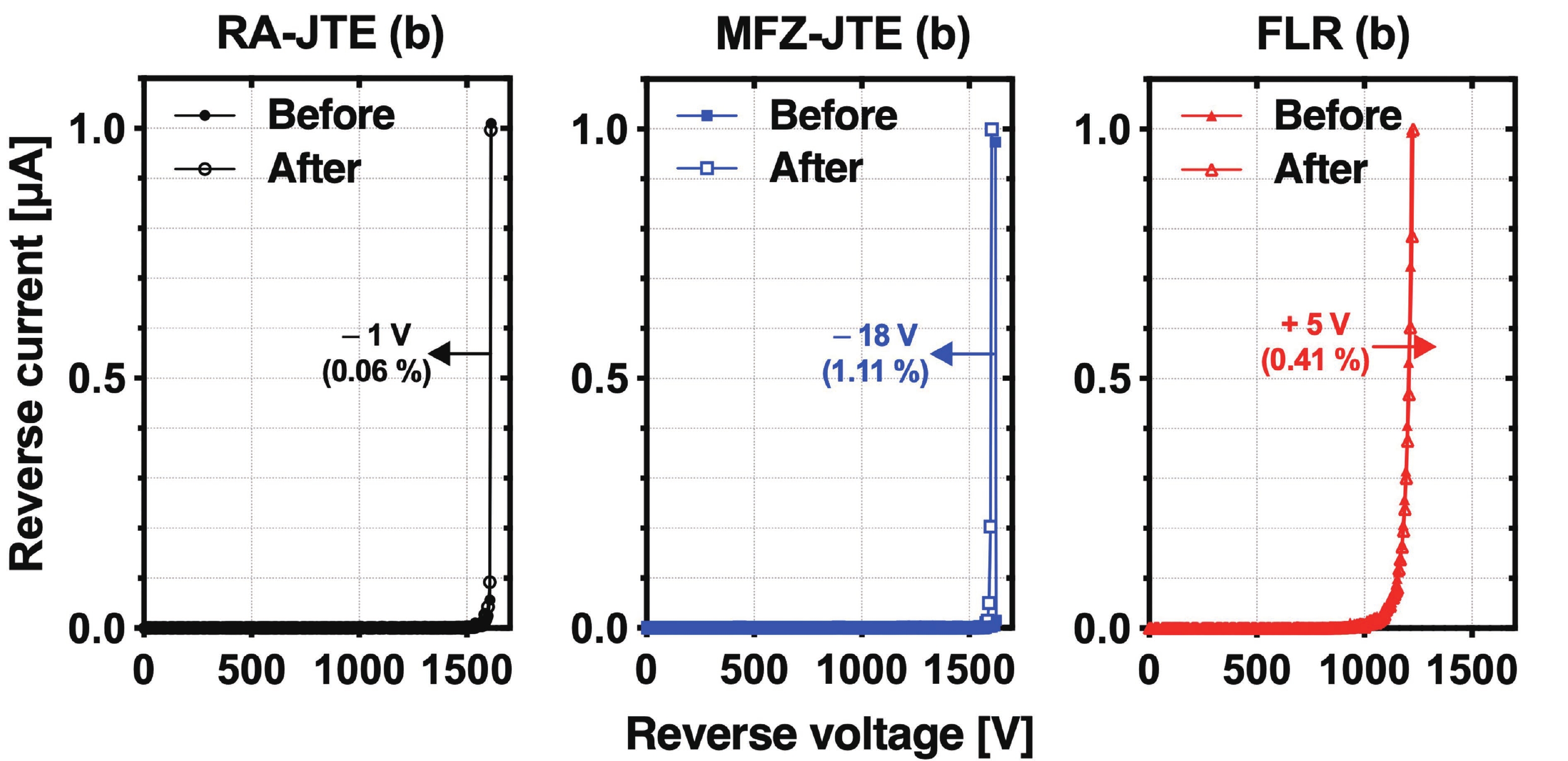
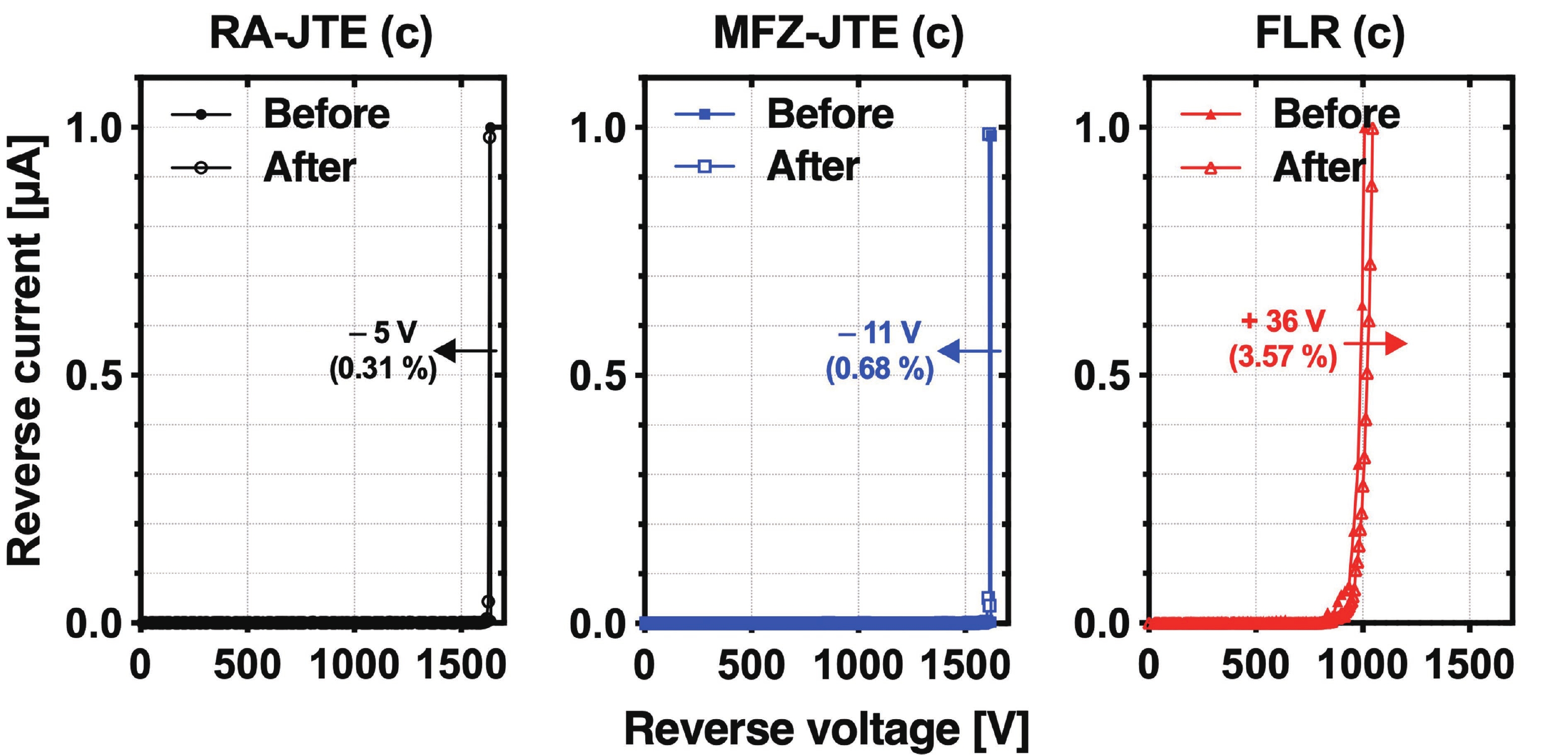
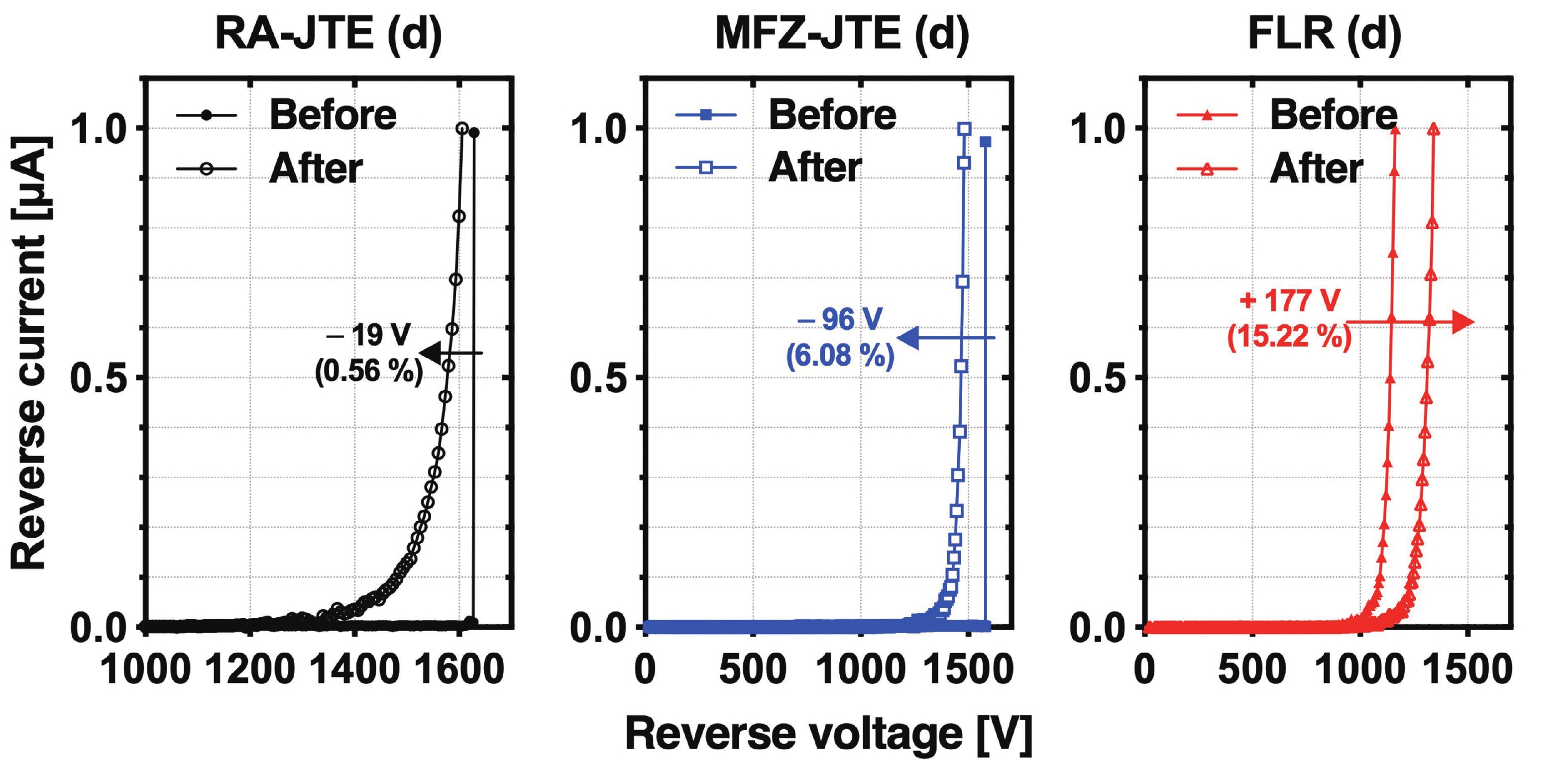
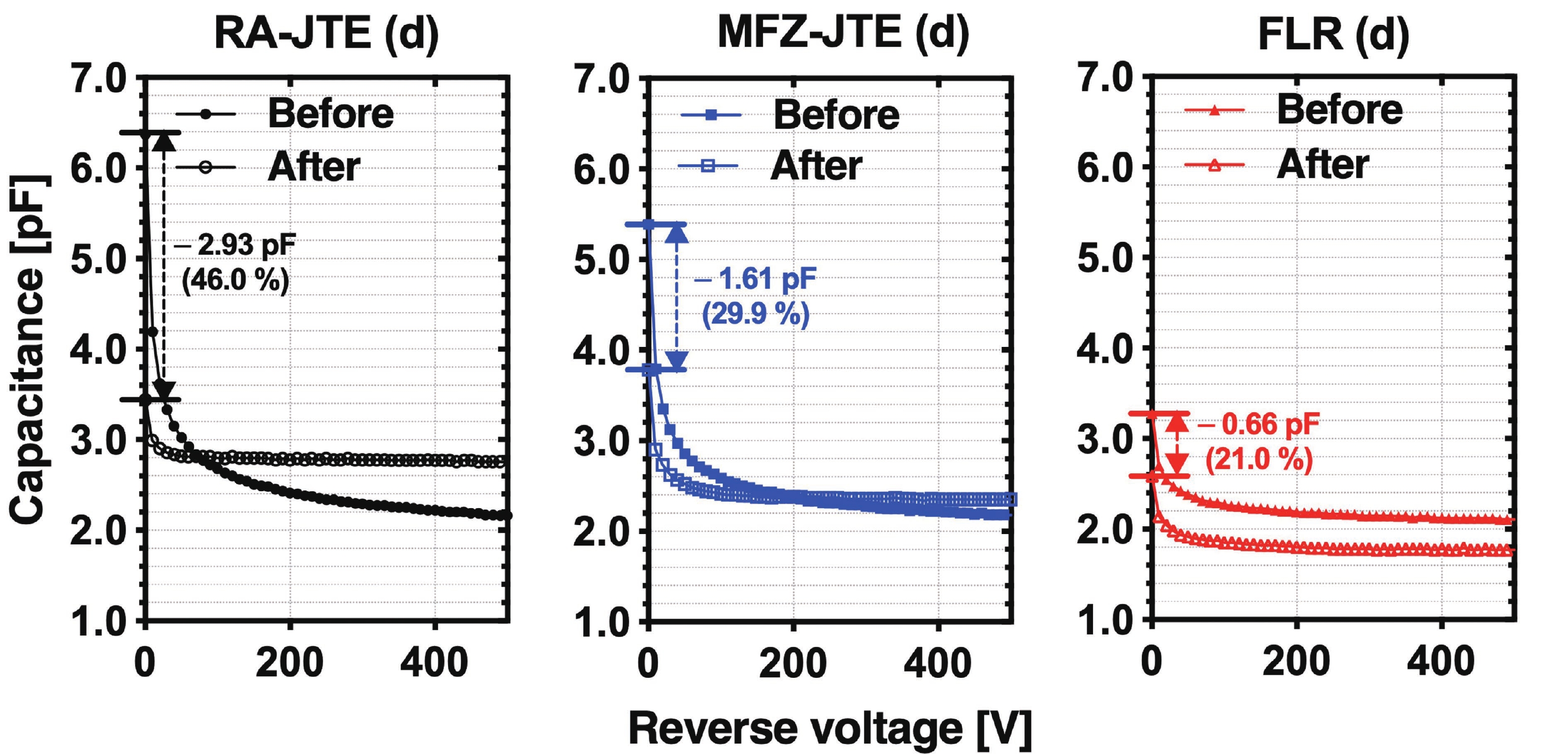
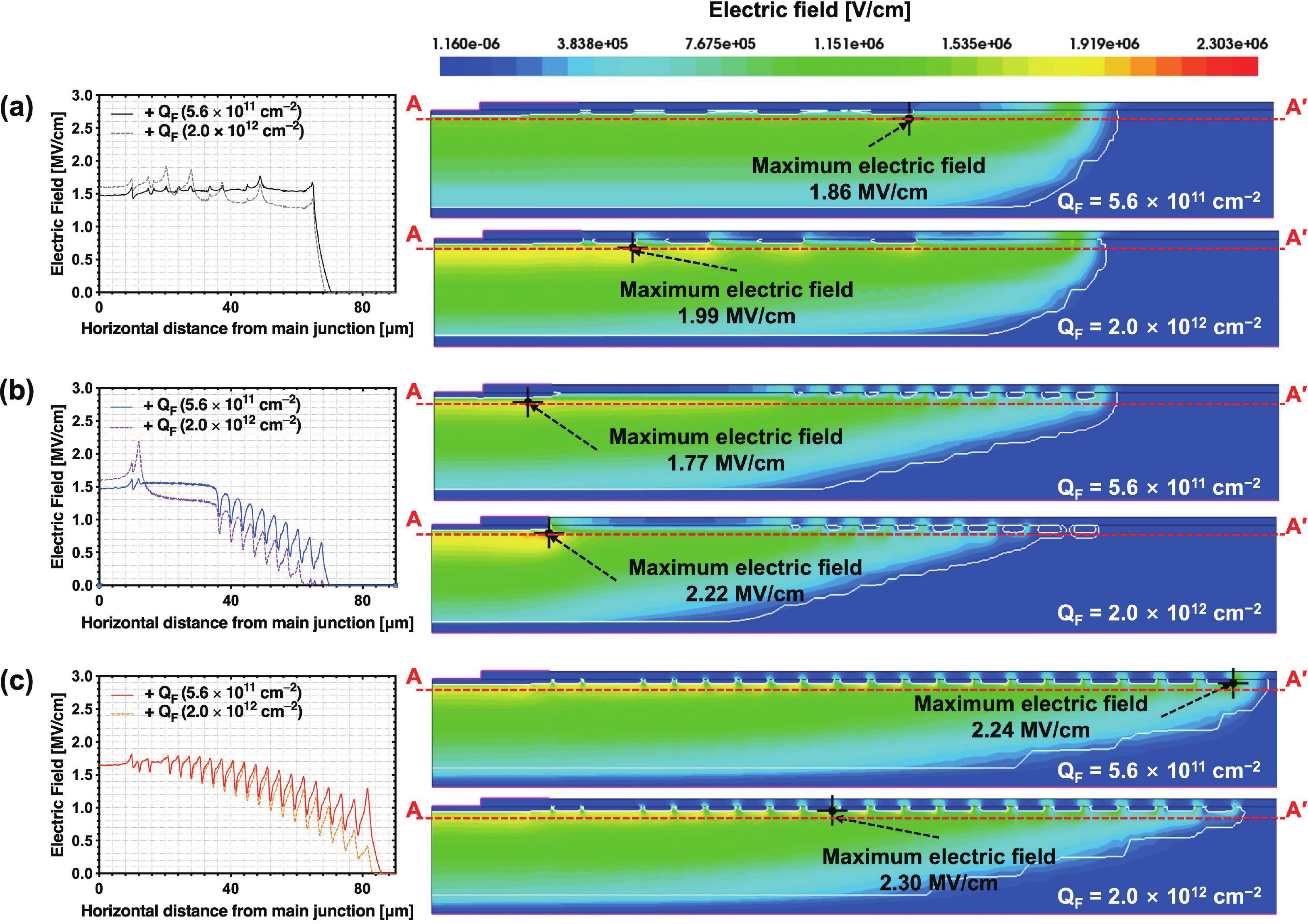
Table 1. Optimized specifications for each edge termination.
| Structures | Wtotal [μm] |
Wring [μm] |
Wd [μm] |
S1 [μm] |
Si [μm] |
Nring |
| RA-JTE | 50 | 4 | − | 1.5 | 2 | 4 |
| MFZ-JTE | 60 | 2.9−1.6 | 0.1 | 0.5 | 0.1 | 14 |
| FLR | 70 | 1.5 | − | 1 | 2 | 20 |
 DownLoad: CSV
Table 2. Sample name and conditions of irradiation.
| Sample | Energy [MeV] | Fluence [cm−2] |
| RA-JTE (a) | 45 | 1 × 10¹² |
| MFZ-JTE (a) | 45 | 1 × 10¹² |
| FLR(a) | 45 | 1 × 10¹² |
| RA-JTE (b) | 45 | 1 × 10¹³ |
| MFZ-JTE (b) | 45 | 1 × 10¹³ |
| FLR (b) | 45 | 1 × 10¹³ |
| RA-JTE (c) | 45 | 1 × 10¹⁴ |
| MFZ-JTE (c) | 45 | 1 × 10¹⁴ |
| FLR (c) | 45 | 1 × 10¹⁴ |
DownLoad: CSV
| [1] |
Fard M T, He J B, Huang H, et al. Aircraft distributed electric propulsion technologies: A review. IEEE Trans Transp Electrif, 2022, 8(4): 4067 doi: 10.1109/TTE.2022.3197332
|
| [2] |
Felgemacher C, Araújo S V, Zacharias P, et al. Cosmic radiation ruggedness of Si and SiC power semiconductors. 2016 28th International Symposium on Power Semiconductor Devices and ICs (ISPSD), 2016: 51 doi: 10.1109/ISPSD.2016.7520775
|
| [3] |
Wang D, Hemming S, Yang Y H, et al. Multilevel inverters for electric aircraft applications: Current status and future trends. IEEE Trans Transp Electrif, 2024, 10(2): 3258 doi: 10.1109/TTE.2023.3296284
|
| [4] |
Dobynde M, Harikumaran J, Guo J N, et al. Cosmic radiation reliability analysis for aircraft power electronics. IEEE Trans Transp Electrif, 2024, 10(1): 344 doi: 10.1109/TTE.2023.3278319
|
| [5] |
Harikumaran J, Buticchi G, Migliazza G, et al. Failure modes and reliability oriented system design for aerospace power electronic converters. IEEE Open J Ind Electron Soc, 2020, 2: 53 doi: 10.1109/OJIES.2020.3047201
|
| [6] |
Yu Q K, Ali W, Cao S, et al. Application of total ionizing dose radiation test standards to SiC MOSFETs. IEEE Trans Nucl Sci, 2022, 69(5): 1127 doi: 10.1109/TNS.2021.3135123
|
| [7] |
Baba T, Ahmed Siddiqui N, Bte Saidin N, et al. Radiation-induced degradation of silicon carbide MOSFETs–A review. Mater Sci Eng B, 2024, 300: 117096 doi: 10.1016/j.mseb.2023.117096
|
| [8] |
Peng C, Lei Z F, Zhang Z G, et al. Bias and temperature dependence of radiation-induced degradation for SiC MOSFETs. IEEE Trans Nucl Sci, 2024, 71(5): 1186 doi: 10.1109/TNS.2024.3384767
|
| [9] |
Liang S W, Wu Z Y, Shu L, et al. Observations on ruggedness degradation of planar-gate SiC MOSFETs after total ionizing dose radiation. 2023 IEEE Energy Conversion Congress and Exposition (ECCE), 2023: 5379 doi: 10.1109/ECCE53617.2023.10362840
|
| [10] |
Feng H N, Liang X W, Pu X J, et al. Special degradation effects of 60Co γ-rays irradiation on electrical parameters of SiC MOSFETs. IEEE Trans Nucl Sci, 2023, 70(9): 2165 doi: 10.1109/TNS.2023.3298063
|
| [11] |
Yang S, Liang X W, Cui J W, et al. Impact of switching frequencies on the TID response of SiC power MOSFETs. J Semicond, 2021, 42(8): 082802 doi: 10.1088/1674-4926/42/8/082802
|
| [12] |
Liu T, Ma R Y, Li S H, et al. Comparative investigation on ionizing irradiation- induced threshold voltage degradation for 1200-V DT SiC MOSFET by experiment and simulation. IEEE Trans Nucl Sci, 2024, 71(11): 2386 doi: 10.1109/TNS.2024.3479201
|
| [13] |
Liang X W, Wei Y, Zhang D, et al. Impact of total ionizing dose effects on the threshold voltage hysteresis of SiC MOSFETs. IEEE Trans Electron Devices, 2024, 71(11): 6889 doi: 10.1109/TED.2024.3457572
|
| [14] |
Hazdra P, Popelka S. Displacement damage and total ionisation dose effects on 4H-SiC power devices. IET Power Electron, 2019, 12(15): 3910 doi: 10.1049/iet-pel.2019.0049
|
| [15] |
Siddiqui A, Hallén A, Usman M. Proton Irradiation-Induced Displacement Damage in 650 V Si and SiC Power Diodes. Phys Status Solidi A, 2023, 220(21): 2300300 doi: 10.1002/pssa.202300300
|
| [16] |
Lin Y X, Chao D S, Liang J H, et al. Electrical deterioration of 4H-SiC MOS capacitors due to bulk and interface traps induced by proton irradiation. Microelectron Reliab, 2023, 142: 114927 doi: 10.1016/j.microrel.2023.114927
|
| [17] |
Sozzi G, Sapienza S, Chiorboli G, et al. Carrier lifetime dependence on temperature and proton irradiation in 4H-SiC device: An experimental law. IEEE Access, 2024, 12: 74230 doi: 10.1109/ACCESS.2024.3405382
|
| [18] |
Chao D S, Shih H Y, Jiang J Y, et al. Influence of displacement damage induced by neutron irradiation on effective carrier density in 4H-SiC SBDs and MOSFETs. Jpn J Appl Phys, 2019, 58: SBBD08 doi: 10.7567/1347-4065/aafc9b
|
| [19] |
Grome C A, Ji W. A brief review of single-event burnout failure mechanisms and design tolerances of silicon carbide power MOSFETs. Electronics, 2024, 13(8): 1414 doi: 10.3390/electronics13081414
|
| [20] |
Witulski A F, Ball D R, Galloway K F, et al. Single-event burnout mechanisms in SiC power MOSFETs. IEEE Trans Nucl Sci, 2018, 65(8): 1951 doi: 10.1109/TNS.2018.2849405
|
| [21] |
Ball D R, Galloway K F, Johnson R A, et al. Effects of breakdown voltage on single-event burnout tolerance of high-voltage SiC power MOSFETs. IEEE Trans Nucl Sci, 2021, 68(7): 1430 doi: 10.1109/TNS.2021.3079846
|
| [22] |
Peng C, Lei Z F, Zhang Z G, et al. Influence of temperature on atmospheric neutron-induced SEB failure rate for SiC MOSFETs. IEEE Trans Nucl Sci, 2024, 71(2): 160 doi: 10.1109/TNS.2023.3348108
|
| [23] |
Wang Y, Zhou J C, Lin M, et al. A comparative study of single-event-burnout for 4H-SiC UMOSFET. IEEE J Electron Devices Soc, 2022, 10: 373 doi: 10.1109/JEDS.2022.3158810
|
| [24] |
Iannaccone G, Sbrana C, Morelli I, et al. Power electronics based on wide-bandgap semiconductors: Opportunities and challenges. IEEE Access, 2021, 9: 139446 doi: 10.1109/ACCESS.2021.3118897
|
| [25] |
Spaziani L, Lu L. Silicon, GaN and SiC: There’s room for all: An application space overview of device considerations. 2018 IEEE 30th International Symposium on Power Semiconductor Devices and ICs (ISPSD), 2018: 8 doi: 10.1109/ISPSD.2018.8393590
|
| [26] |
Casady J B, Johnson R W. Status of silicon carbide (SiC) as a wide-bandgap semiconductor for high-temperature applications: A review. Solid State Electron, 1996, 39(10): 1409 doi: 10.1016/0038-1101(96)00045-7
|
| [27] |
Lauenstein J M, Casey M C, Ladbury R L, et al. Space radiation effects on SiC power device reliability. 2021 IEEE International Reliability Physics Symposium (IRPS), 2021: 1 doi: 10.1109/IRPS46558.2021.9405180
|
| [28] |
Pearton S J, Aitkaliyeva A, Xian M H, et al. Review: Radiation damage in wide and ultra-wide bandgap semiconductors. ECS J Solid State Sci Technol, 2021, 10(5): 055008 doi: 10.1149/2162-8777/abfc23
|
| [29] |
Rafí J M, Pellegrini G, Godignon P, et al. Electron, neutron, and proton irradiation effects on SiC radiation detectors. IEEE Trans Nucl Sci, 2020, 67(12): 2481 doi: 10.1109/TNS.2020.3029730
|
| [30] |
Witczak S C, Martin W A, Palko J W, et al. Displacement damage in an irradiated 4H-SiC MESFET. IEEE Trans Nucl Sci, 2025, 72(5): 1755 doi: 10.1109/TNS.2025.3550298
|
| [31] |
Zeng Q, Yang Z C, Wang X F, et al. Research progress on radiation damage mechanism of SiC MOSFETs under various irradiation conditions. IEEE Trans Electron Devices, 2024, 71(3): 1718 doi: 10.1109/TED.2024.3359172
|
| [32] |
Pérez R, Mestres N, Blanqué S, et al. A highly effective edge termination design for SiC planar high power devices. Mater Sci Forum, 2004, 457/458/459/460: 1253 doi: 10.4028/www.scientific.net/MSF.457-460.1253
|
| [33] |
Sung W, Van Brunt E, Baliga B J, et al. A new edge termination technique for high-voltage devices in 4H-SiC–multiple-floating-zone junction termination extension. IEEE Electron Device Lett, 2011, 32(7): 880 doi: 10.1109/LED.2011.2144561
|
| [34] |
Hirao T, Onose H, Kan Y S, et al. Edge termination with enhanced field-limiting rings insensitive to surface charge for high-voltage SiC power devices. IEEE Trans Electron Devices, 2020, 67(7): 2850 doi: 10.1109/TED.2020.2992577
|
| [35] |
Tan B, Tian X L, Lu J, et al. Design and optimization of four-region multistep field limiting rings for 10kV 4H-SiC IGBTs. 2018 14th IEEE International Conference on Solid-State and Integrated Circuit Technology (ICSICT), 2018: 1 doi: 10.1109/ICSICT.2018.8565661
|
| [36] |
Deng X C, Xu S D, Zhang B, et al. A near ideal edge termination technique for ultrahigh-voltage 4H-SiC devices with multi-zone gradient field limiting ring. 2018 1st Workshop on Wide Bandgap Power Devices and Applications in Asia (WiPDA Asia), 2018: 144 doi: 10.1109/WiPDAAsia.2018.8734553
|
| [37] |
Broderick L Z, Moult J, Rusch O, et al. Highly efficient floating field rings for SiC power electronic devices-A systematic experimental study. Key Eng Mater, 2023, 946: 103 doi: 10.4028/p-0z5887
|
| [38] |
Wen Y, Xu X J, Zhu H, et al. Design and characteristics of an etching field limiting ring for 10kV SiC power device. 2019 16th China International Forum on Solid State Lighting & 2019 International Forum on Wide Bandgap Semiconductors China (SSLChina: IFWS), 2019: 37 doi: 10.1109/SSLChinaIFWS49075.2019.9019780
|
| [39] |
Kim C, Yoon H, Kim D S, et al. Comparison analysis of radiation effects on 1.2 kV SiC metal-oxide-semiconductor field-effect transistors with gamma-ray and proton irradiation. Electronics, 2024, 13(7): 1352 doi: 10.3390/electronics13071352
|


Article views: 1611 Times PDF downloads: 309 Times Cited by: 0 Times
Received: 21 April 2025 Revised: 04 August 2025 Online: Accepted Manuscript: 18 August 2025Uncorrected proof: 19 August 2025Published: 15 January 2026
| Citation: |
Sangyeob Kim, Jeongtae Kim, Dong-Seok Kim, Hyuncheol Bae, Min-Woo Ha, Ogyun Seok. Radiation hardness of 1.2 kV SiC power devices with advanced edge termination structures under proton irradiation[J]. Journal of Semiconductors, 2026, 47(1): 012501. doi: 10.1088/1674-4926/25040023
****
S Kim, J Kim, D S Kim, H Bae, M W Ha, and O Seok, Radiation hardness of 1.2 kV SiC power devices with advanced edge termination structures under proton irradiation[J]. J. Semicond., 2026, 47(1): 012501 doi: 10.1088/1674-4926/25040023

|
 Sangyeob Kim received the B.S. degree in Electronic Engineering in 2023 and the M.S. degree in Semiconductor System Engineering in 2025 from Kumoh National Institute of Technology, Gumi, Korea. Since 2025, he has been pursuing a Ph.D. degree in Department of Electrical and Electronic Engineering at Pusan National University, Busan, Korea. His research interests include the design and fabrication of high-voltage power semiconductor devices based on silicon carbide (SiC)
 Jeongtae Kim received the B.S. degree (2024) in School of Electronic Engineering from Kumoh National Institute of Technology, Gumi, Korea. Since 2024, He is a master’s degree candidate in the Department of Semiconductor System Engineering from Kumoh National Institute of Technology. His research interests include radiation effect on semiconductor devices
 Dong-Seok Kim received the B.S., the M.S., and the Ph.D degrees in electronics engineering from Kyungpook National University (KNU), Republic of Korea, in 2008, 2010, and 2015, respectively. His doctoral research concerned the growth of Ⅲ-nitride epitaxial structure and the fabrication of GaN-based devices. He is currently a senior researcher of Korea Atomic Energy Research Insitute (KAERI). His current research is focused on the radiation effect on semiconductor devices such as HEMT, MOSFET, TFT, etc., and the radiation-utilized applications such as nuclear battery and sensors
 Hyuncheol Bae received the B.S. and M.S. degrees in electrical engineering from Dongguk University, Seoul, Republic of Korea, in 1999 and 2001, respectively, and the Ph.D. degree in electrical engineering from Chungnam National University, Daejeon, Republic of Korea, in 2009. He has been with the Electronics and Telecommunications Research Institute (ETRI), Daejeon, Republic of Korea, since 2001, where he is currently serving as a Principal Researcher. From 2018 to 2024, he also served as a Professor in the Department of Advanced Device Engineering at the University of Science and Technology (UST), Daejeon, Republic of Korea. His research has focused on semiconductor device packaging. His current research interests include power module packaging for electric vehicles (xEV), RF packaging for 5G/6G communication systems, and hermetic packaging for aerospace applications
 Min-Woo Ha received the B.S. degree (2001) from Korea Advanced Institute of Science and Technology, Daejon, Korea and the Ph.D. degree (2007) from Seoul National University, Seoul, Korea. He was a Senior Engineer with System LSI division at Samsung Electronics, Yongin, Korea from 2007 to 2009. He worked for Korea Electronics Technology Institute, Korea from 2009 to 2013. In 2013, he joined the University of Texas at Dallas, Richardson, U.S.A as a Research Scientist. Since 2014, he has been with Myongji University, Yongin, Korea, where he is a Professor in Department of Electrical Engineering. He has published 70 papers in international journals. His research interests include Si power transistors, Ⅲ−Ⅴ devices, SiC MOSFETs, and multilayer ceramic capacitors
 Ogyun Seok received his Ph.D. degree (2013) in Electrical and Computer Engineering from Seoul National University, Seoul, Republic of Korea. From 2013 to 2014, he was a Postdoctoral Researcher in the Department of Electrical and Computer Engineering at University of Illinois at Urbana-Champaign, Champaign, IL, United States. From 2014 to 2020, he joined the Power Semiconductor Research Center at the Korea Electrotechnology Research Institute, Changwon, Republic of Korea as a Senior Researcher. From 2020 to 2024, he was an Assistant Professor in the School of Electronic Engineering in Kumoh National Institute of Technology, Gumi, Republic of Korea. Since 2024, he has been with Pusan National University, Busan, Republic of Korea, as an assistant professor in the School of Electrical & Electronic Engineering. He currently develops power semiconductor devices including SiC planar MOSFETs, SiC P−i−N diodes, SiC super-junction diodes, and GaN HEMTs
| [1] |
Fard M T, He J B, Huang H, et al. Aircraft distributed electric propulsion technologies: A review. IEEE Trans Transp Electrif, 2022, 8(4): 4067 doi: 10.1109/TTE.2022.3197332
|
| [2] |
Felgemacher C, Araújo S V, Zacharias P, et al. Cosmic radiation ruggedness of Si and SiC power semiconductors. 2016 28th International Symposium on Power Semiconductor Devices and ICs (ISPSD), 2016: 51 doi: 10.1109/ISPSD.2016.7520775
|
| [3] |
Wang D, Hemming S, Yang Y H, et al. Multilevel inverters for electric aircraft applications: Current status and future trends. IEEE Trans Transp Electrif, 2024, 10(2): 3258 doi: 10.1109/TTE.2023.3296284
|
| [4] |
Dobynde M, Harikumaran J, Guo J N, et al. Cosmic radiation reliability analysis for aircraft power electronics. IEEE Trans Transp Electrif, 2024, 10(1): 344 doi: 10.1109/TTE.2023.3278319
|
| [5] |
Harikumaran J, Buticchi G, Migliazza G, et al. Failure modes and reliability oriented system design for aerospace power electronic converters. IEEE Open J Ind Electron Soc, 2020, 2: 53 doi: 10.1109/OJIES.2020.3047201
|
| [6] |
Yu Q K, Ali W, Cao S, et al. Application of total ionizing dose radiation test standards to SiC MOSFETs. IEEE Trans Nucl Sci, 2022, 69(5): 1127 doi: 10.1109/TNS.2021.3135123
|
| [7] |
Baba T, Ahmed Siddiqui N, Bte Saidin N, et al. Radiation-induced degradation of silicon carbide MOSFETs–A review. Mater Sci Eng B, 2024, 300: 117096 doi: 10.1016/j.mseb.2023.117096
|
| [8] |
Peng C, Lei Z F, Zhang Z G, et al. Bias and temperature dependence of radiation-induced degradation for SiC MOSFETs. IEEE Trans Nucl Sci, 2024, 71(5): 1186 doi: 10.1109/TNS.2024.3384767
|
| [9] |
Liang S W, Wu Z Y, Shu L, et al. Observations on ruggedness degradation of planar-gate SiC MOSFETs after total ionizing dose radiation. 2023 IEEE Energy Conversion Congress and Exposition (ECCE), 2023: 5379 doi: 10.1109/ECCE53617.2023.10362840
|
| [10] |
Feng H N, Liang X W, Pu X J, et al. Special degradation effects of 60Co γ-rays irradiation on electrical parameters of SiC MOSFETs. IEEE Trans Nucl Sci, 2023, 70(9): 2165 doi: 10.1109/TNS.2023.3298063
|
| [11] |
Yang S, Liang X W, Cui J W, et al. Impact of switching frequencies on the TID response of SiC power MOSFETs. J Semicond, 2021, 42(8): 082802 doi: 10.1088/1674-4926/42/8/082802
|
| [12] |
Liu T, Ma R Y, Li S H, et al. Comparative investigation on ionizing irradiation- induced threshold voltage degradation for 1200-V DT SiC MOSFET by experiment and simulation. IEEE Trans Nucl Sci, 2024, 71(11): 2386 doi: 10.1109/TNS.2024.3479201
|
| [13] |
Liang X W, Wei Y, Zhang D, et al. Impact of total ionizing dose effects on the threshold voltage hysteresis of SiC MOSFETs. IEEE Trans Electron Devices, 2024, 71(11): 6889 doi: 10.1109/TED.2024.3457572
|
| [14] |
Hazdra P, Popelka S. Displacement damage and total ionisation dose effects on 4H-SiC power devices. IET Power Electron, 2019, 12(15): 3910 doi: 10.1049/iet-pel.2019.0049
|
| [15] |
Siddiqui A, Hallén A, Usman M. Proton Irradiation-Induced Displacement Damage in 650 V Si and SiC Power Diodes. Phys Status Solidi A, 2023, 220(21): 2300300 doi: 10.1002/pssa.202300300
|
| [16] |
Lin Y X, Chao D S, Liang J H, et al. Electrical deterioration of 4H-SiC MOS capacitors due to bulk and interface traps induced by proton irradiation. Microelectron Reliab, 2023, 142: 114927 doi: 10.1016/j.microrel.2023.114927
|
| [17] |
Sozzi G, Sapienza S, Chiorboli G, et al. Carrier lifetime dependence on temperature and proton irradiation in 4H-SiC device: An experimental law. IEEE Access, 2024, 12: 74230 doi: 10.1109/ACCESS.2024.3405382
|
| [18] |
Chao D S, Shih H Y, Jiang J Y, et al. Influence of displacement damage induced by neutron irradiation on effective carrier density in 4H-SiC SBDs and MOSFETs. Jpn J Appl Phys, 2019, 58: SBBD08 doi: 10.7567/1347-4065/aafc9b
|
| [19] |
Grome C A, Ji W. A brief review of single-event burnout failure mechanisms and design tolerances of silicon carbide power MOSFETs. Electronics, 2024, 13(8): 1414 doi: 10.3390/electronics13081414
|
| [20] |
Witulski A F, Ball D R, Galloway K F, et al. Single-event burnout mechanisms in SiC power MOSFETs. IEEE Trans Nucl Sci, 2018, 65(8): 1951 doi: 10.1109/TNS.2018.2849405
|
| [21] |
Ball D R, Galloway K F, Johnson R A, et al. Effects of breakdown voltage on single-event burnout tolerance of high-voltage SiC power MOSFETs. IEEE Trans Nucl Sci, 2021, 68(7): 1430 doi: 10.1109/TNS.2021.3079846
|
| [22] |
Peng C, Lei Z F, Zhang Z G, et al. Influence of temperature on atmospheric neutron-induced SEB failure rate for SiC MOSFETs. IEEE Trans Nucl Sci, 2024, 71(2): 160 doi: 10.1109/TNS.2023.3348108
|
| [23] |
Wang Y, Zhou J C, Lin M, et al. A comparative study of single-event-burnout for 4H-SiC UMOSFET. IEEE J Electron Devices Soc, 2022, 10: 373 doi: 10.1109/JEDS.2022.3158810
|
| [24] |
Iannaccone G, Sbrana C, Morelli I, et al. Power electronics based on wide-bandgap semiconductors: Opportunities and challenges. IEEE Access, 2021, 9: 139446 doi: 10.1109/ACCESS.2021.3118897
|
| [25] |
Spaziani L, Lu L. Silicon, GaN and SiC: There’s room for all: An application space overview of device considerations. 2018 IEEE 30th International Symposium on Power Semiconductor Devices and ICs (ISPSD), 2018: 8 doi: 10.1109/ISPSD.2018.8393590
|
| [26] |
Casady J B, Johnson R W. Status of silicon carbide (SiC) as a wide-bandgap semiconductor for high-temperature applications: A review. Solid State Electron, 1996, 39(10): 1409 doi: 10.1016/0038-1101(96)00045-7
|
| [27] |
Lauenstein J M, Casey M C, Ladbury R L, et al. Space radiation effects on SiC power device reliability. 2021 IEEE International Reliability Physics Symposium (IRPS), 2021: 1 doi: 10.1109/IRPS46558.2021.9405180
|
| [28] |
Pearton S J, Aitkaliyeva A, Xian M H, et al. Review: Radiation damage in wide and ultra-wide bandgap semiconductors. ECS J Solid State Sci Technol, 2021, 10(5): 055008 doi: 10.1149/2162-8777/abfc23
|
| [29] |
Rafí J M, Pellegrini G, Godignon P, et al. Electron, neutron, and proton irradiation effects on SiC radiation detectors. IEEE Trans Nucl Sci, 2020, 67(12): 2481 doi: 10.1109/TNS.2020.3029730
|
| [30] |
Witczak S C, Martin W A, Palko J W, et al. Displacement damage in an irradiated 4H-SiC MESFET. IEEE Trans Nucl Sci, 2025, 72(5): 1755 doi: 10.1109/TNS.2025.3550298
|
| [31] |
Zeng Q, Yang Z C, Wang X F, et al. Research progress on radiation damage mechanism of SiC MOSFETs under various irradiation conditions. IEEE Trans Electron Devices, 2024, 71(3): 1718 doi: 10.1109/TED.2024.3359172
|
| [32] |
Pérez R, Mestres N, Blanqué S, et al. A highly effective edge termination design for SiC planar high power devices. Mater Sci Forum, 2004, 457/458/459/460: 1253 doi: 10.4028/www.scientific.net/MSF.457-460.1253
|
| [33] |
Sung W, Van Brunt E, Baliga B J, et al. A new edge termination technique for high-voltage devices in 4H-SiC–multiple-floating-zone junction termination extension. IEEE Electron Device Lett, 2011, 32(7): 880 doi: 10.1109/LED.2011.2144561
|
| [34] |
Hirao T, Onose H, Kan Y S, et al. Edge termination with enhanced field-limiting rings insensitive to surface charge for high-voltage SiC power devices. IEEE Trans Electron Devices, 2020, 67(7): 2850 doi: 10.1109/TED.2020.2992577
|
| [35] |
Tan B, Tian X L, Lu J, et al. Design and optimization of four-region multistep field limiting rings for 10kV 4H-SiC IGBTs. 2018 14th IEEE International Conference on Solid-State and Integrated Circuit Technology (ICSICT), 2018: 1 doi: 10.1109/ICSICT.2018.8565661
|
| [36] |
Deng X C, Xu S D, Zhang B, et al. A near ideal edge termination technique for ultrahigh-voltage 4H-SiC devices with multi-zone gradient field limiting ring. 2018 1st Workshop on Wide Bandgap Power Devices and Applications in Asia (WiPDA Asia), 2018: 144 doi: 10.1109/WiPDAAsia.2018.8734553
|
| [37] |
Broderick L Z, Moult J, Rusch O, et al. Highly efficient floating field rings for SiC power electronic devices-A systematic experimental study. Key Eng Mater, 2023, 946: 103 doi: 10.4028/p-0z5887
|
| [38] |
Wen Y, Xu X J, Zhu H, et al. Design and characteristics of an etching field limiting ring for 10kV SiC power device. 2019 16th China International Forum on Solid State Lighting & 2019 International Forum on Wide Bandgap Semiconductors China (SSLChina: IFWS), 2019: 37 doi: 10.1109/SSLChinaIFWS49075.2019.9019780
|
| [39] |
Kim C, Yoon H, Kim D S, et al. Comparison analysis of radiation effects on 1.2 kV SiC metal-oxide-semiconductor field-effect transistors with gamma-ray and proton irradiation. Electronics, 2024, 13(7): 1352 doi: 10.3390/electronics13071352
|

 WeChat ID
Journal of Semiconductors © 2017 All Rights Reserved 京ICP备05085259号-2


