- • Uncorrected proofs: articles that have been copy edited and formatted, but have not been finalized yet. They still need to be proof-read and corrected by the author(s) and the text could still change before final publication.
- • Corrected proofs: articles that contain the authors' corrections. Final citation details, e.g. volume and/or issue number, publication year and page numbers, still need to be added and the text might change before final publication.
There are two types in Press articles:
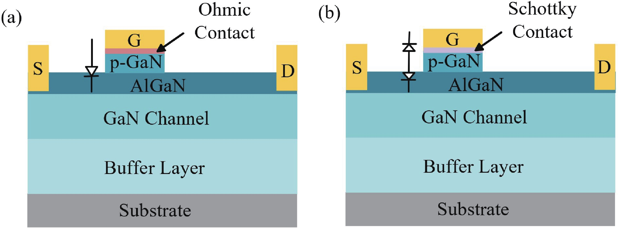
In this paper, a novel gate-series-diode structure for the Schottky-type p-GaN HEMTs is proposed, and the impact of the proposed structure on gate−source voltage oscillation is investigated when the device is turned on. The proposed structure is capable of effectively mitigating the gate−source voltage overshoot problem of GaN device, and has little effect on the switching characteristics. The gate voltage oscillations can be greatly stabilized at the steady-state turn-on voltage level when the turn-on voltage is 5 V. Compared with the conventional structure, the overshoots of the proposed structure reduce by 31.4%−71.4% and 40.6%−80.4% respectively under the two pulses, as drain−source voltage rises. The proposed structure is proved to be a potential method on improving gate reliability of the most GaN power devices.
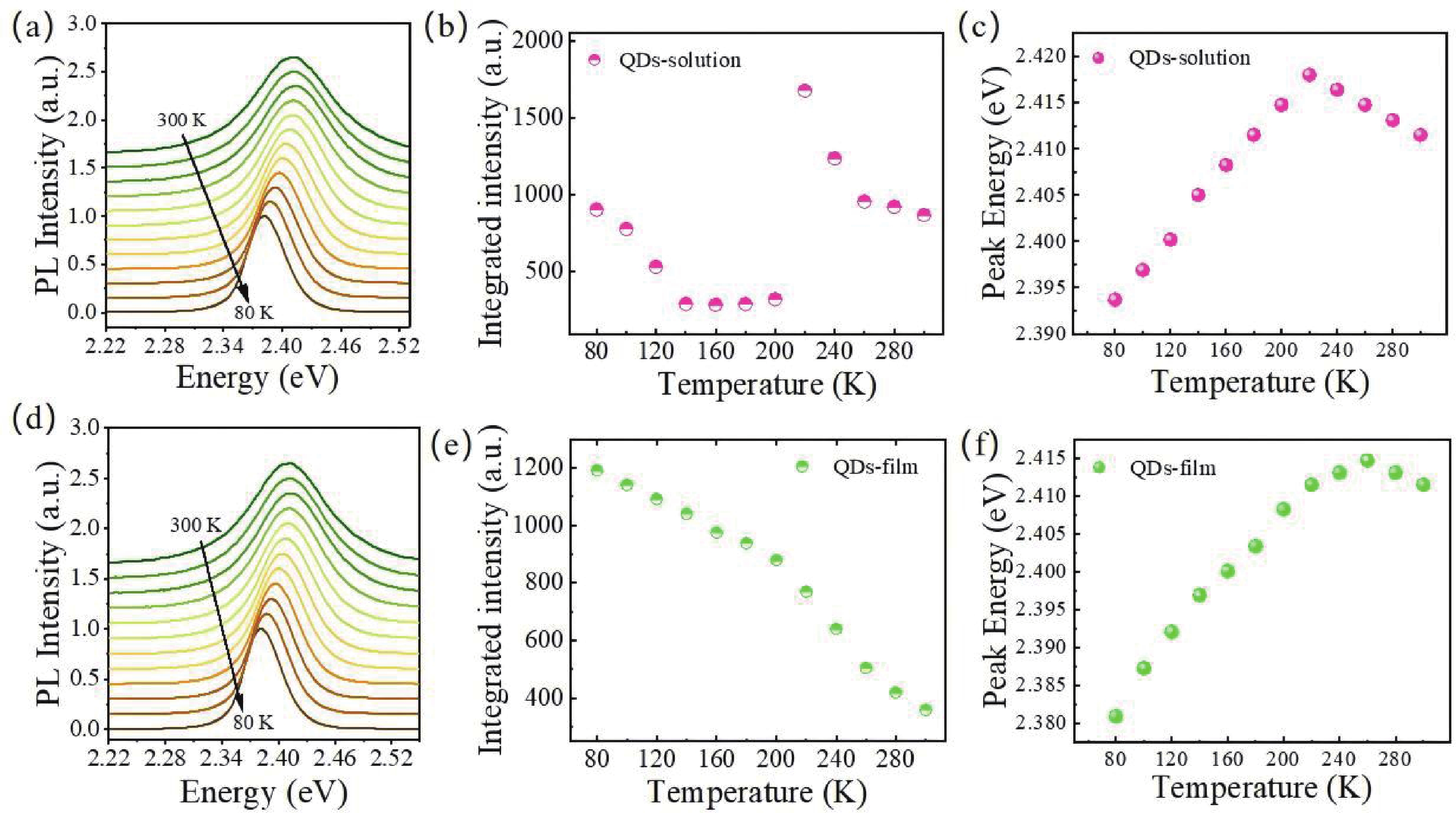
Temperature dependent photoluminescence (PL) and time-resolved PL (TRPL) of CsPbBr3 quantum dots (QDs) in solution and film are investigated. The electron−phonon coupling strength of quantum dots in solution is found two times larger than that of thin films. The averaged phonon energy involved in luminescence is also significantly higher than that of thin films, indicating that ligands’ phonons are involved in optical processes in solution but not in film. TRPL shows that the luminescence lifetime of the solution (22.5 ns) is longer than that of the thin film (5 ns) at room temperature, and both decrease abnormally with decreasing temperature, ascribing to the thermally activated trap states for PL, the further analysis shows that the trap energy levels in the thin film are deeper (~20 meV) compared to ~4 meV in solution. Our work proves that the morphology of organic ligands can regulate electron−phonon interactions and optoelectronic properties in CsPbBr3 QDs, providing fundamental insights into its photophysics.
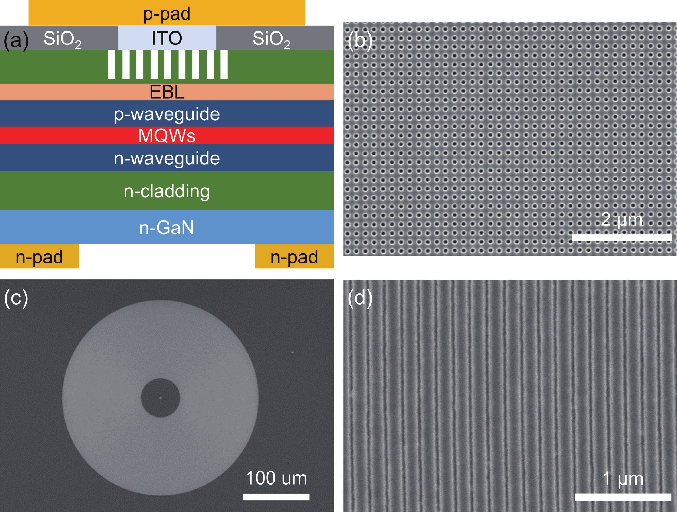
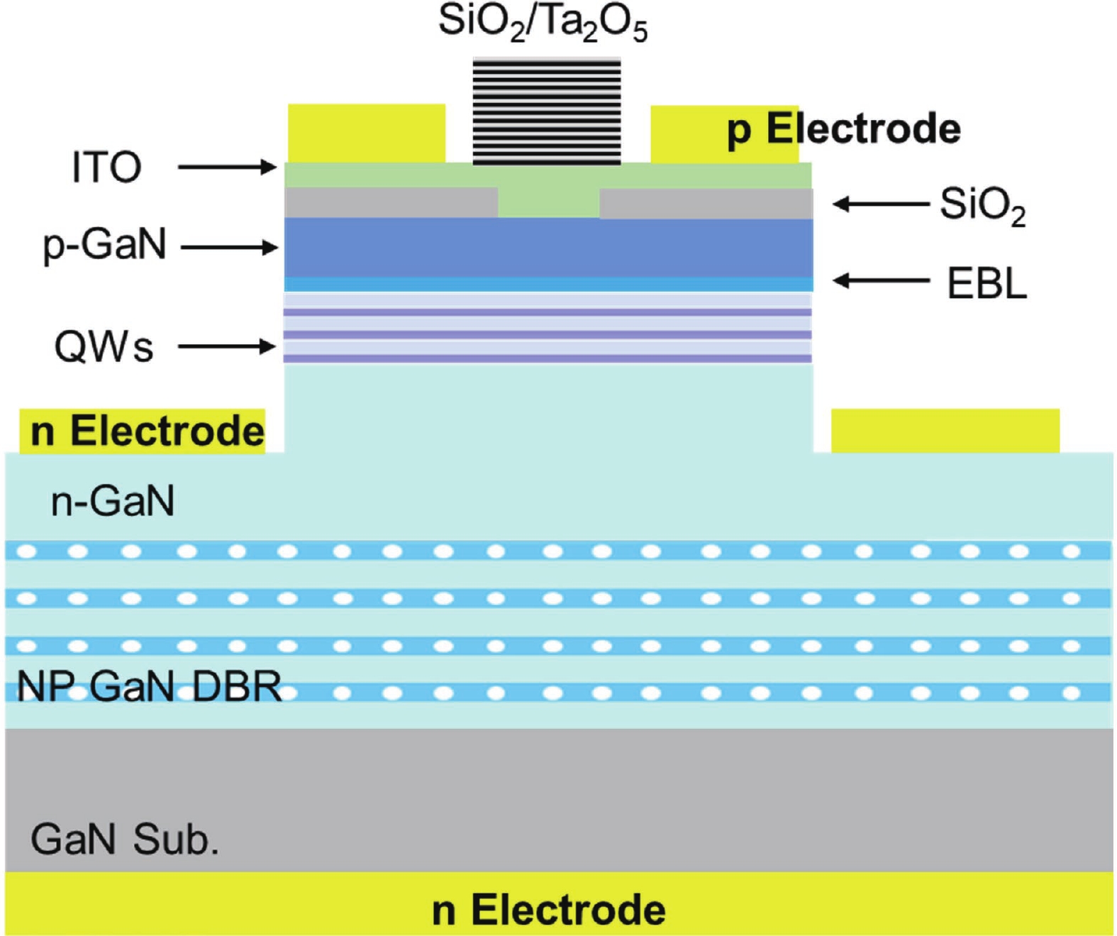
We demonstrate room-temperature pulsed lasing of two types of GaN-based surface emitting lasers (SEL) fabricated without epitaxial regrowth. We present a direct comparison between a circular grating (CGSEL) and a photonic crystal (PCSEL) design. The devices are realized by etching the photonic structures directly into the p-GaN cladding, and utilizing a patterned indium tin oxide (ITO) top contact. Both designs exhibit lasing near 438 nm under pulsed current injection. The CGSEL, incorporating a central defect, achieves a low threshold current density (<1 kA/cm2) and a small divergence angle (≈0.15°) by coupling to a bandgap defect mode. In contrast, the PCSEL shows a higher threshold current density and lases on a 1D band-edge mode, resulting in a cross-shaped far-field pattern. These results confirm the regrowth-free method as a viable route for manufacturable GaN SELs. Crucially, the comparative study identifies the CGSEL defect-mode design as a more robust path toward high-performance lasing in low-confinement epitaxial structures.
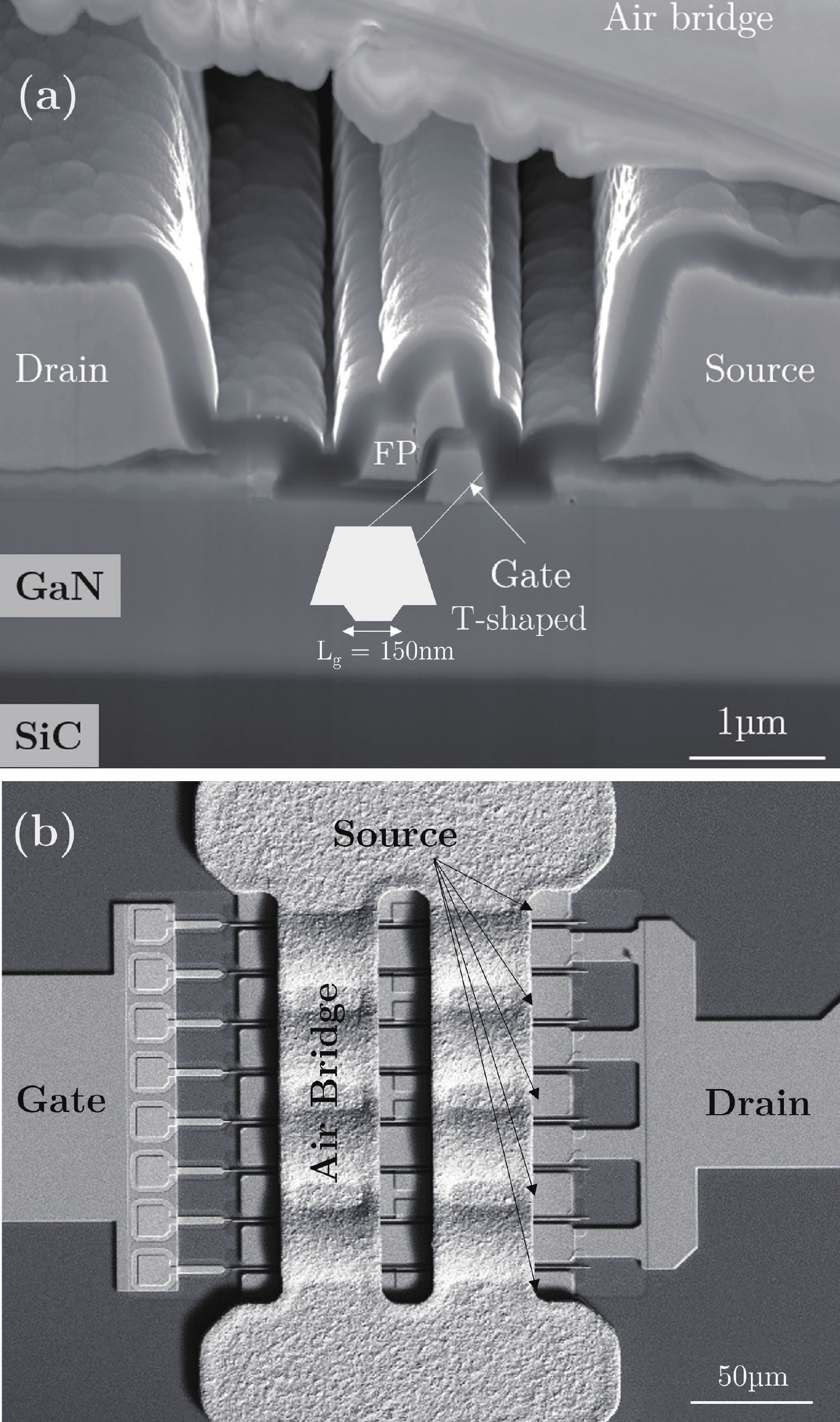
This work focuses on the early-life drift mechanisms in 150 nm AlGaN/GaN HEMTs on SiC under RF-HTOL stress at 9 GHz and 130 °C. Electrical measurements during the first hours of stress reveal significant shifts in threshold voltage, transconductance, and drain lag, indicating the activation of deep traps located in the buffer. A transient increase in gate leakage current is also observed under reverse gate bias, suggesting additional trapping or conduction paths at the AlGaN/SiN or cap/passivation interface. These electrical instabilities coincide with a progressive degradation of RF performance, notably in gain and power-added efficiency. Electroluminescence measurements further support the presence of electrically active defects, with distinct spatial patterns depending on the bias configuration.
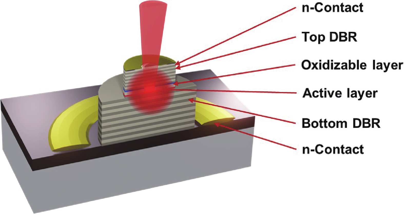
A high-speed single-mode vertical-cavity surface-emitting laser (VCSEL) is one of the most important light sources for optical interconnects in data centers. Single-mode VCSEL can improve the transmission distance. In this letter, we demonstrate a single-mode 850 nm VCSEL with a bit rate of 60 Gb/s under NRZ modulation and 104 Gb/s under PAM4 modulation across a 100 m length of OM5 fiber, without the need for equalization or a filter. In addition, by using optical injection locking, the 3 dB bandwidth is enhanced to 68.5 GHz.
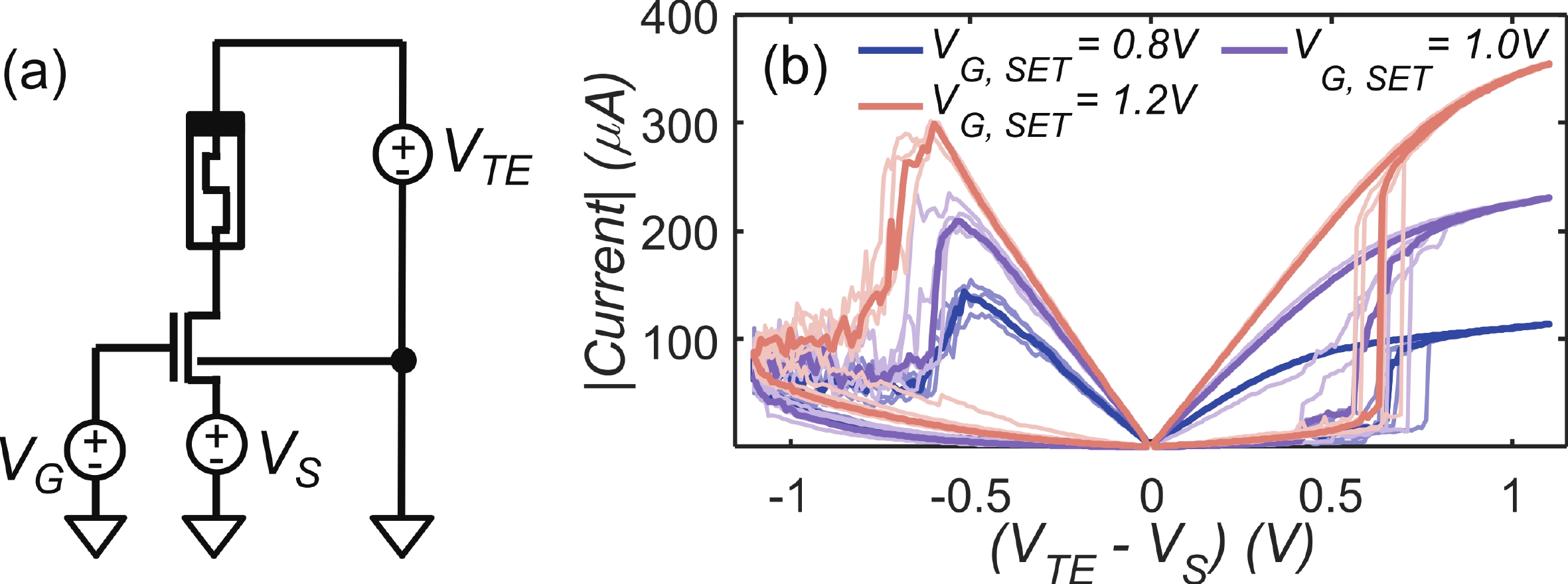
Resistive random access memories (RRAMs) are emerging as a key enabling technology for cost-effective, energy-efficient and secure chips, especially in the framework of edge computing. In particular, their electrically programmable resistance has been widely exploited in several in-memory computing and neuromorphic architectures. By adjusting the applied voltages and compliance currents (IC), RRAM devices can be programmed to multiple resistance states during set and reset procedures, enabling multilevel functionality. While the multilevel behavior of the reset phase is generally well captured by existing compact models, only a few account for the multilevel characteristics of the set operations. Moreover, such models are rarely validated against comprehensive experimental datasets capturing device dynamics across multiple timescales. In this work, we present a physics-based compact model that enhances the UniMORE RRAM framework by incorporating the dynamic lateral evolution of the conductive filament (CF), thereby enabling accurate simulation of set operations at varying IC values. The model is calibrated to experimental data from IHP 130 nm 1T1R RRAM technology and reproduces device behavior across several operating conditions using a single set of parameters. The results highlight the potential of the proposed compact model in design optimization workflows of RRAM-based circuits.
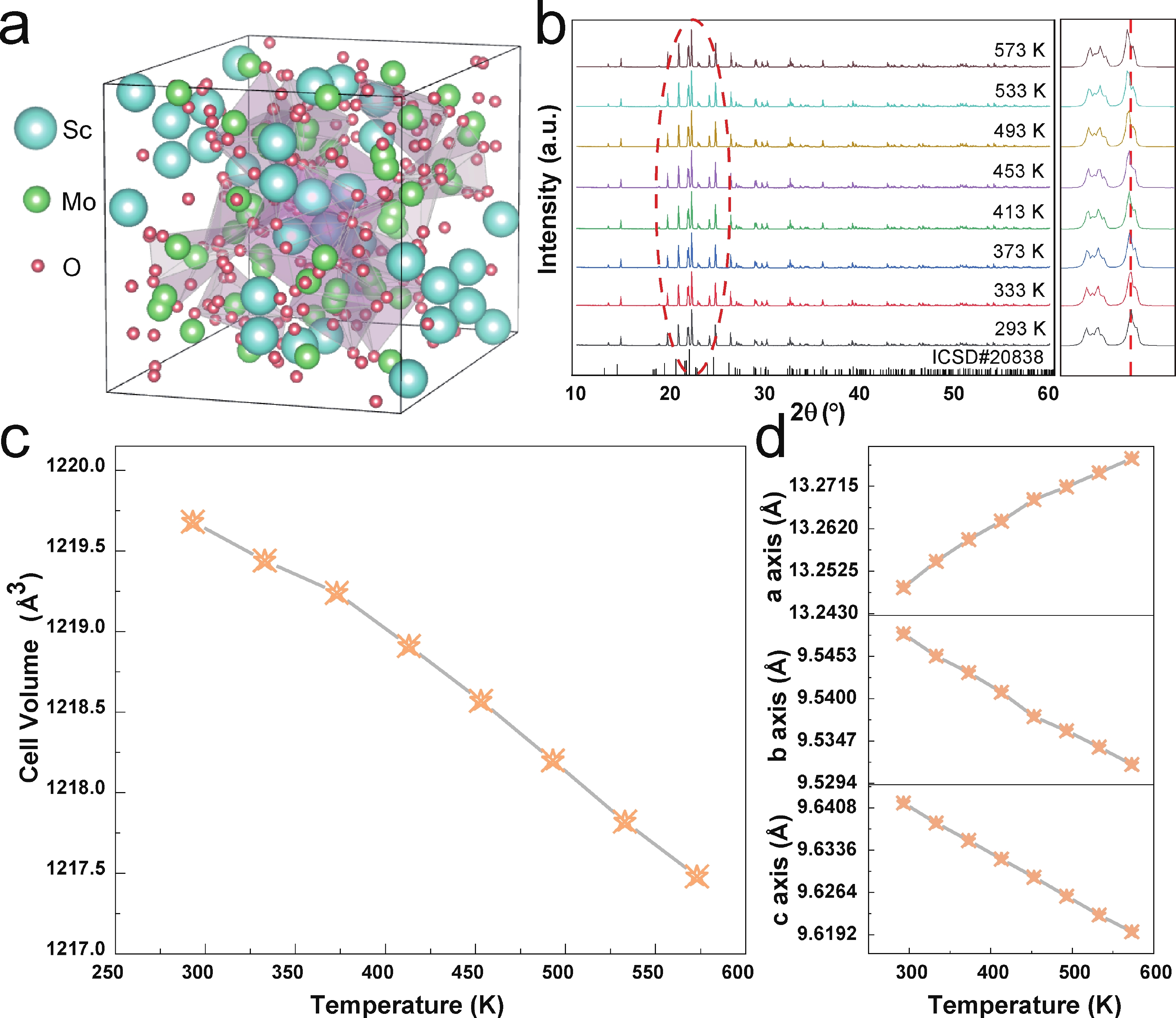
Fluorescence temperature sensing technology has become a research direction in the field of temperature measurement with its significant advantages of non-contact measurement, high spatial resolution, fast response and anti-electromagnetic interference. Although the double rare earth ion doping ratio fluorescent temperature sensing materials have made significant progress, the thermal quenching phenomenon is still the key bottleneck restricting its performance improvement. In this study, we propose to construct a flexible Sc2Mo3O12:Eu3+/Tb3+ film with negative thermal expansion characteristics, and systematically study its visual temperature sensing characteristics. The negative thermal expansion characteristics of Sc2Mo3O12 matrix effectively inhibited the thermal quenching rate of Tb3+ luminescence, and enhanced the thermal enhanced luminescence effect of Eu3+. This two-way regulation mechanism improves the intensity comparison of the two light-emitting channels, and provides an innovative strategy for improving the sensitivity of temperature sensing. The flexible film based on Eu3+/Tb3+ codoped system realizes intuitive temperature perception through the significant change of fluorescent color, and can complete the temperature interpretation without complex spectral equipment. This greatly expands its application prospect in the field of rapid field detection and real-time monitoring, and shows its broad potential in the fields of wearable devices, biomedical diagnosis, and real-time monitoring of surface temperature field.
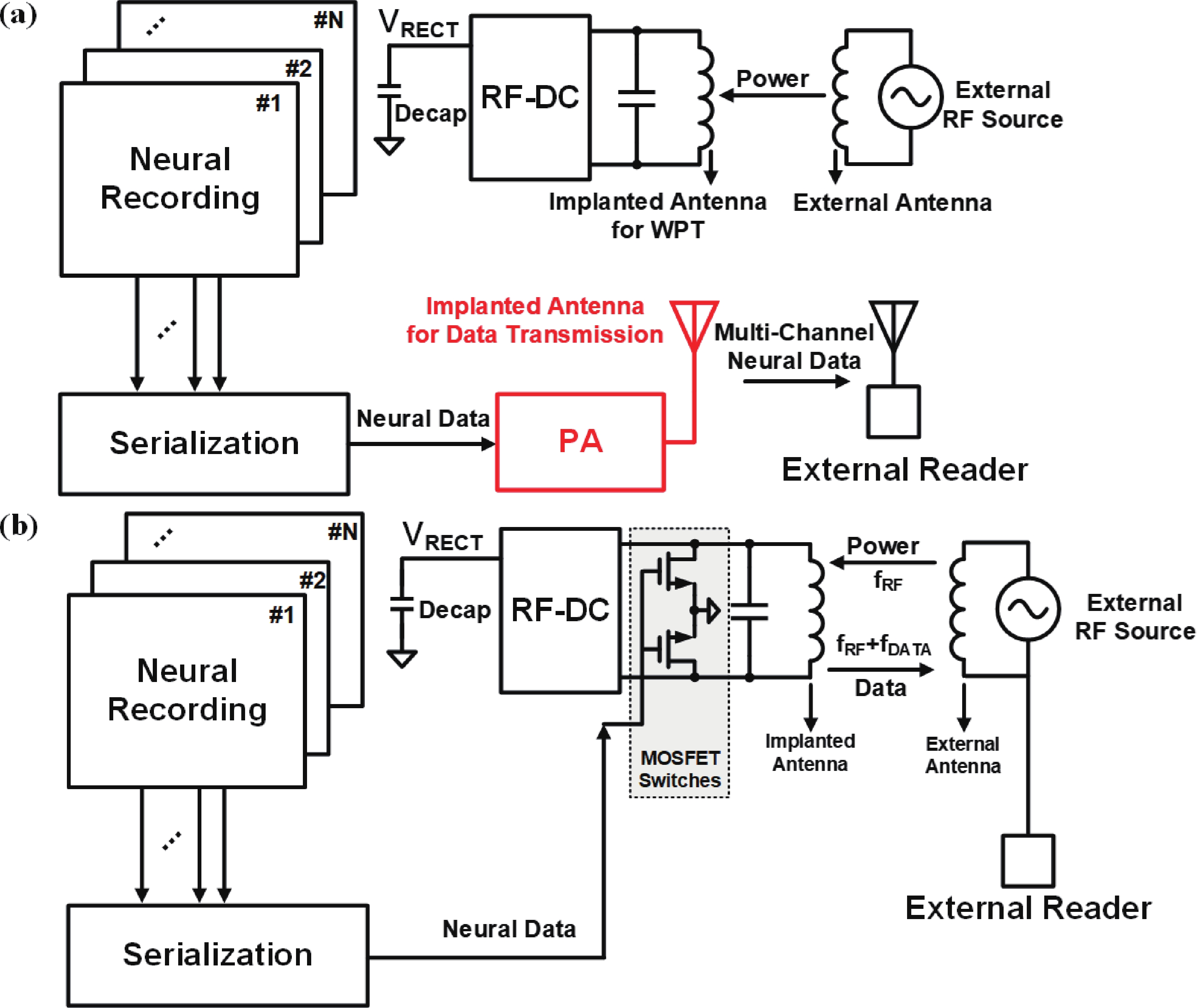
Battery-free radio systems utilizing wireless power transfer (WPT) further facilitate the miniaturization of neural implants. However, simultaneous monitoring of multiple neuronal activities is required to obtain high-fidelity neural signals. Consequently, the integration of numerous channels on a single chip and the wireless transmission of massive multi-channel data pose significant challenges for implantable battery-free neural interfaces. This work introduces dual overlapped on-chip antennas to eliminate the need for a battery in the neural implants and enable high-data-rate backscatter for transmitting the massive data acquired simultaneously from 72 channels. Additionally, an orthogonal coding and sampling technique is employed to reduce both power consumption and area per channel. Fabricated in a 65 nm CMOS process, the proposed chip integrates 72 neural recording channels within a 2 mm × 2 mm area and achieves a backscatter data rate of 18 Mbps.
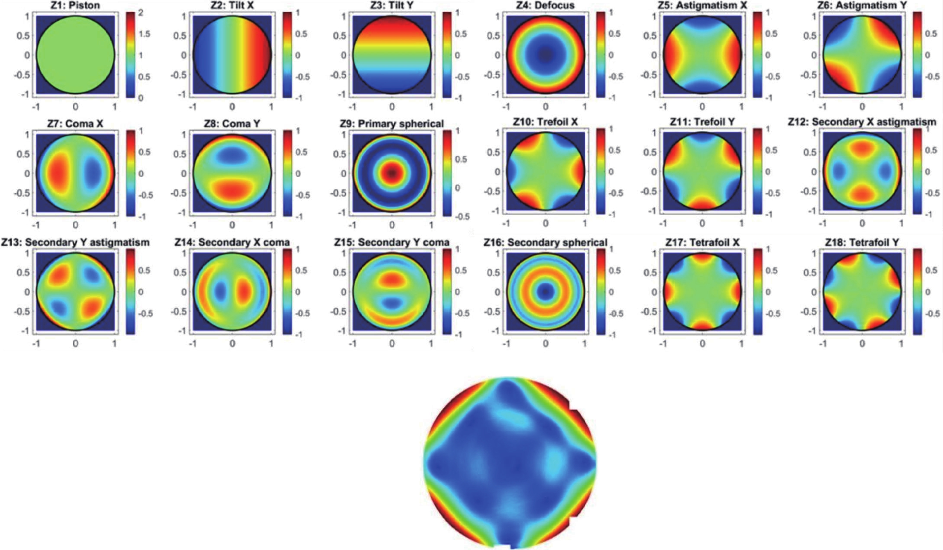
To address the urgent demand for sub-100-nm overlay accuracy in wafer bonding for three-dimensional integration, this study systematically investigates and proposes an extended overlay assessment model that integrates physical mechanisms with data-driven approaches, along with a methodology for analyzing its correlation with process parameters. Conventional rigid-body transformation models fail to effectively characterize systematic deformations induced by crystalline anisotropy and process stresses. To overcome this limitation, this paper constructs an extended overlay model based on Zernike polynomials. By incorporating systematic deformation terms with clear physical significance, the model achieves precise description of non-uniform wafer deformation. Furthermore, an innovative Zernike term selection strategy is proposed, which combines physics-guided pre-screening with stepwise regression optimized by the Akaike Information Criterion (AIC). This strategy effectively resolves issues of model overfitting and underfitting, significantly enhancing the model's generalizability and interpretability while maintaining accuracy. Experimental validation using Patterned Wafer Geometry (PWG) data demonstrates that the proposed model achieves a goodness-of-fit R2 greater than 0.70 for both the net deformation introduced by the bonding process and the lithography-compensable component, showcasing excellent deformation decomposition capability. Further correlation analysis based on multiple sets of process experimental data quantitatively reveals strong correlations (|r| > 0.85) between key process parameters, such as the peak bonding head force, and specific Zernike deformation modes. This provides direct evidence for actively suppressing detrimental deformations through process optimization. This research establishes a complete technical framework encompassing theory, algorithm, experimental verification, and process traceability, laying a crucial theoretical and technical foundation for mechanism diagnosis, predictive compensation, and closed-loop control in high-precision wafer bonding.
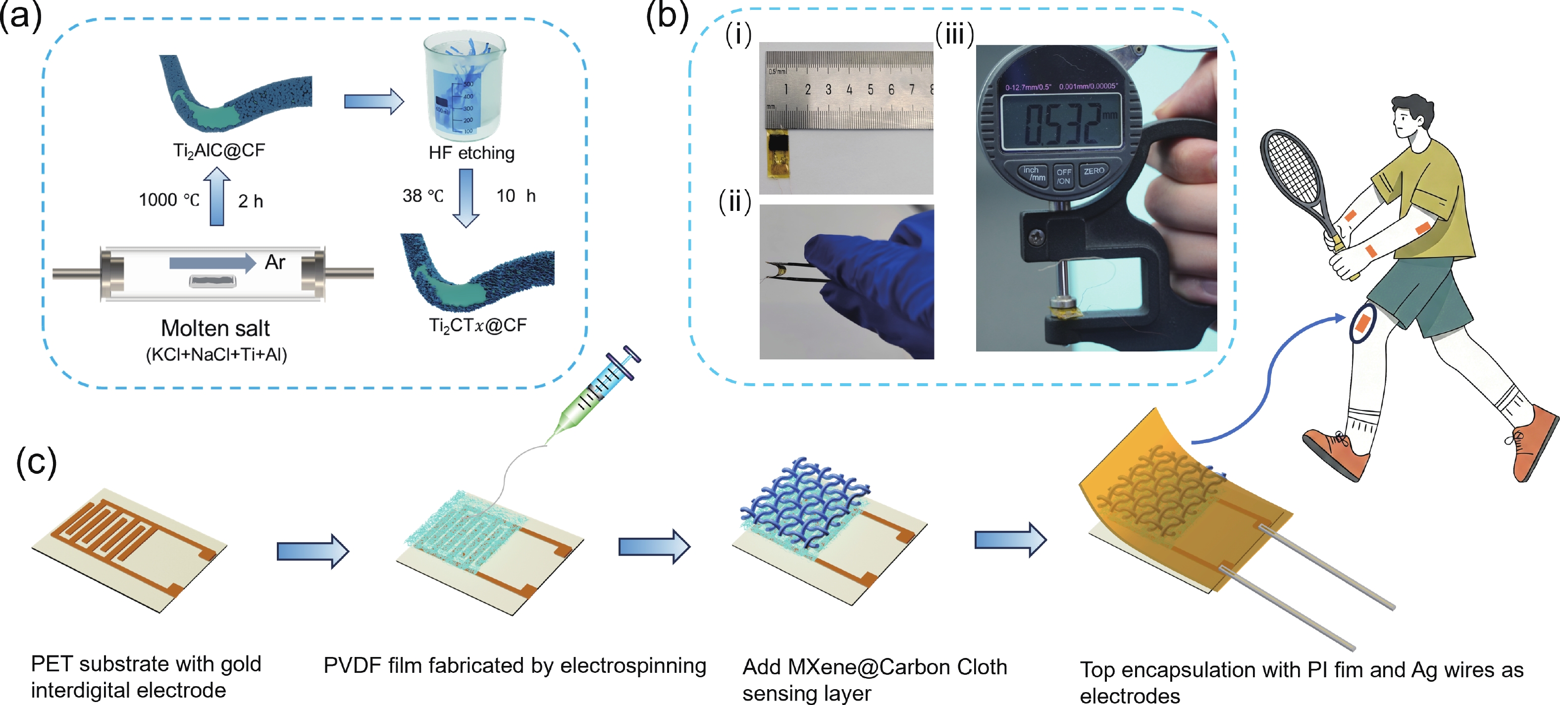
High performance flexible pressure sensors, as a very important group of electronic component for information transmission and collection, have gained widespread attention. Herein, Ti2CTx MXene nanosheets were vertically grown on carbon cloth substrate (Ti2CTx@CC) via the simple sintering and subsequent etching process. Flexible pressure sensors featuring the Ti2CTx MXene nanosheets as the sensitive material were then fabricated using polyvinylidene fluoride (PVDF) film weaved by the electrospinning route between the sensitive material and the interdigital electrodes to improve the sensitivity. As-fabricated flexible sensor exhibited superior performances including high sensitivity up to 3109.2 kPa−1, good response and recovery time of 80/80 ms, and favorable stability over 8000 loading/unloading cycles. Boasting the high sensitivity across a broad range, the sensor can in real-time capture a spectrum of human activities—from the faint pulse signal to the large pressure of joint activities and shows promising capability for mapping spatial pressure distribution.

In fractional-N phase-locked loops, minimizing the integral nonlinearity (INL) of the digital-to-time converter (DTC) is crucial since it directly limits PLL performance. Considering the trade-off between DTC delay range and linearity, this paper presents a fractional-N dual-path SPD/PFD PLL (DP-SPFDPLL) with a complementary DTC pair. Controlled by the complementary control words, two DTCs are introduced before the two inputs of the phase detector for DTC range reduction and INL cancellation. The required DTC range is further halved by using differential VCO outputs to retime the frequency divider output. The overall design collectively achieves a 4× reduction in DTC range requirement. Fabricated in 7 nm FinFET, the DP-SPFDPLL achieves 118 fs RMS jitter and −247.5 dB figure-of-merit.
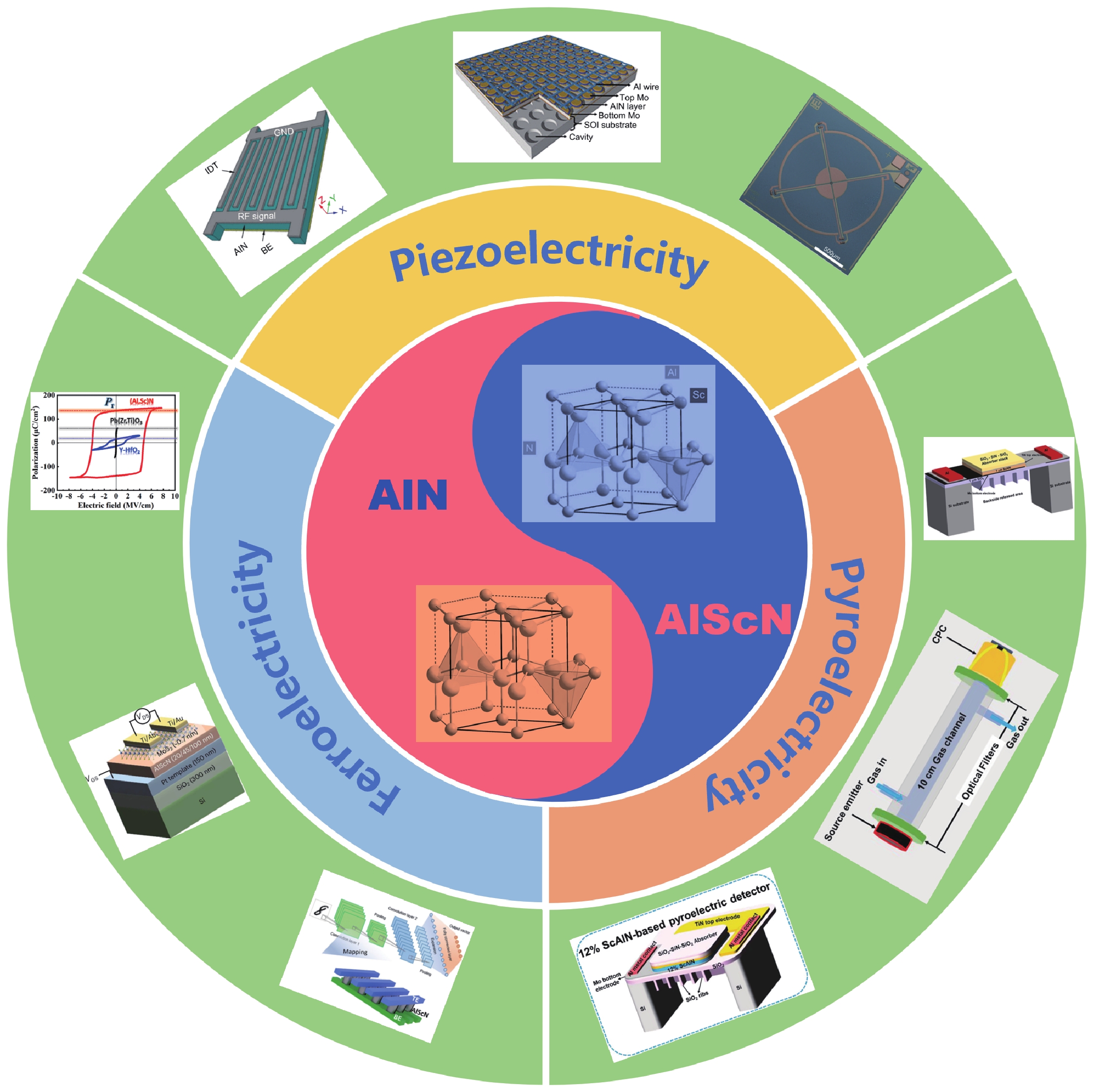
Aluminum scandium nitride (AlScN), an emerging Ⅲ-nitride semiconductor material, has attracted significant attention in recent years due to its exceptional piezoelectric properties, high thermal stability, tunable bandgap, and excellent compatibility with micro/nano fabrication. This paper systematically reviews the crystal structure, fundamental properties, and property modulation mechanisms of AlScN. It also summarizes recent progress in micro/nano fabrication technologies, including deposition, etching, and device integration. Furthermore, the applications of AlScN in diverse fields such as micro-electromechanical systems (MEMS), RF communications, energy conversion, optoelectronics and sensors are discussed. Finally, current challenges and promising future research directions for AlScN are outlined.
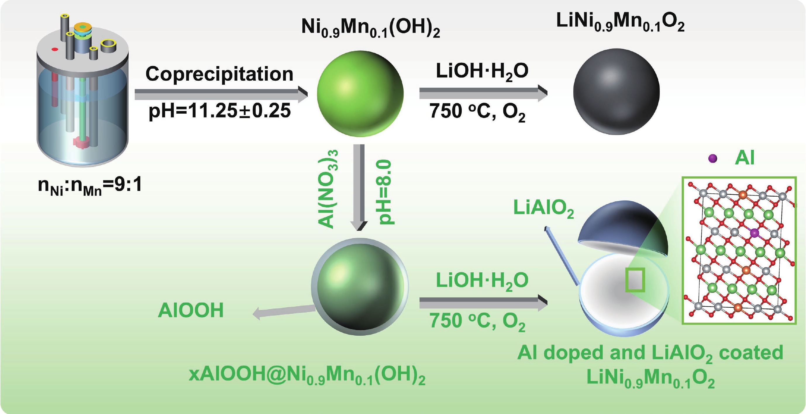
LiNi0.9Mn0.1O2 (LNM91) is a promising cobalt-free, high-energy cathode material for next-generation lithium-ion batteries, but its commercialization is challenged by rapid capacity fading resulting from bulk and interfacial structural degradation. Herein, an in situ surface-to-bulk dual-modification strategy is developed to synthesize 6Al-LNM91 (6 mol% Al modified LNM91) via a one-step calcination process based on Al diffusion chemistry. This method concurrently constructs a protective LiAlO2 coating and incorporates Al3+ into the bulk lattice, effectively enhancing the structural integrity of the cathode during cycling. The optimized 6Al-LNM91 cathode delivers a remarkable rate capability of 165 mA∙h∙g−1 at 10 C and maintains 94.03% capacity retention after 120 cycles at 0.5 C (2.8 − 4.4 V), substantially outperforming the pristine material (76.82% of LNM91). This organic solvent-free, single-step modification approach offers a scalable and efficient route for improving high-nickel layered oxide cathodes.
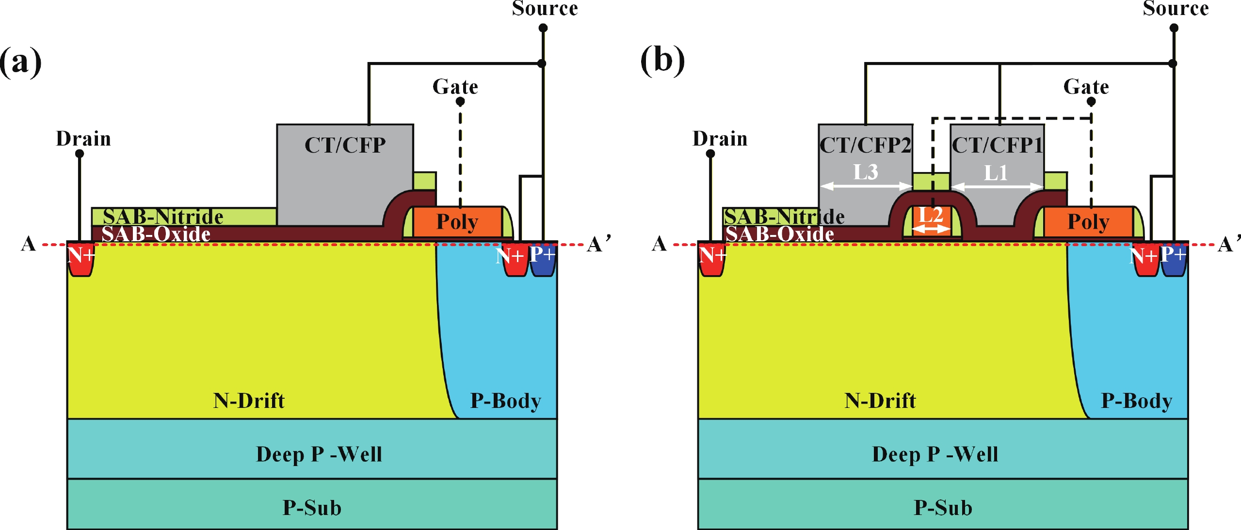
To improve the breakdown voltage (BV)−specific on-resistance (Ron,sp) trade-off and enhance manufacturability, this article proposes a novel lateral diffused metal−oxide−semiconductor (LDMOS) structure that features a split gate and split contact field plate (CFP). This novel structure requires no additional bias voltages, masks, or process steps, making it fully compatible with the bipolar-CMOS-DMOS (BCD) process flow. The physical mechanisms are elucidated through Technology computer-aided design (TCAD) simulations. In the on-state, the positively biased split gate forms an accumulation layer at the drift region surface, thereby reducing Ron,sp. In the off-state, both the split gate and split CFP introduce additional electric-field peaks that smooth the lateral electric field, thus preserving a high BV. Compared with the conventional CFP-LDMOS, the proposed CFP-LDMOS achieves an 8.52% reduction in Ron,sp without compromising BV, leading to an 8.07% improvement in the figure of merit (FOM). Notably, the proposed structure can be extended to LDMOS devices across different voltage levels within BCD platforms, demonstrating its broad applicability.
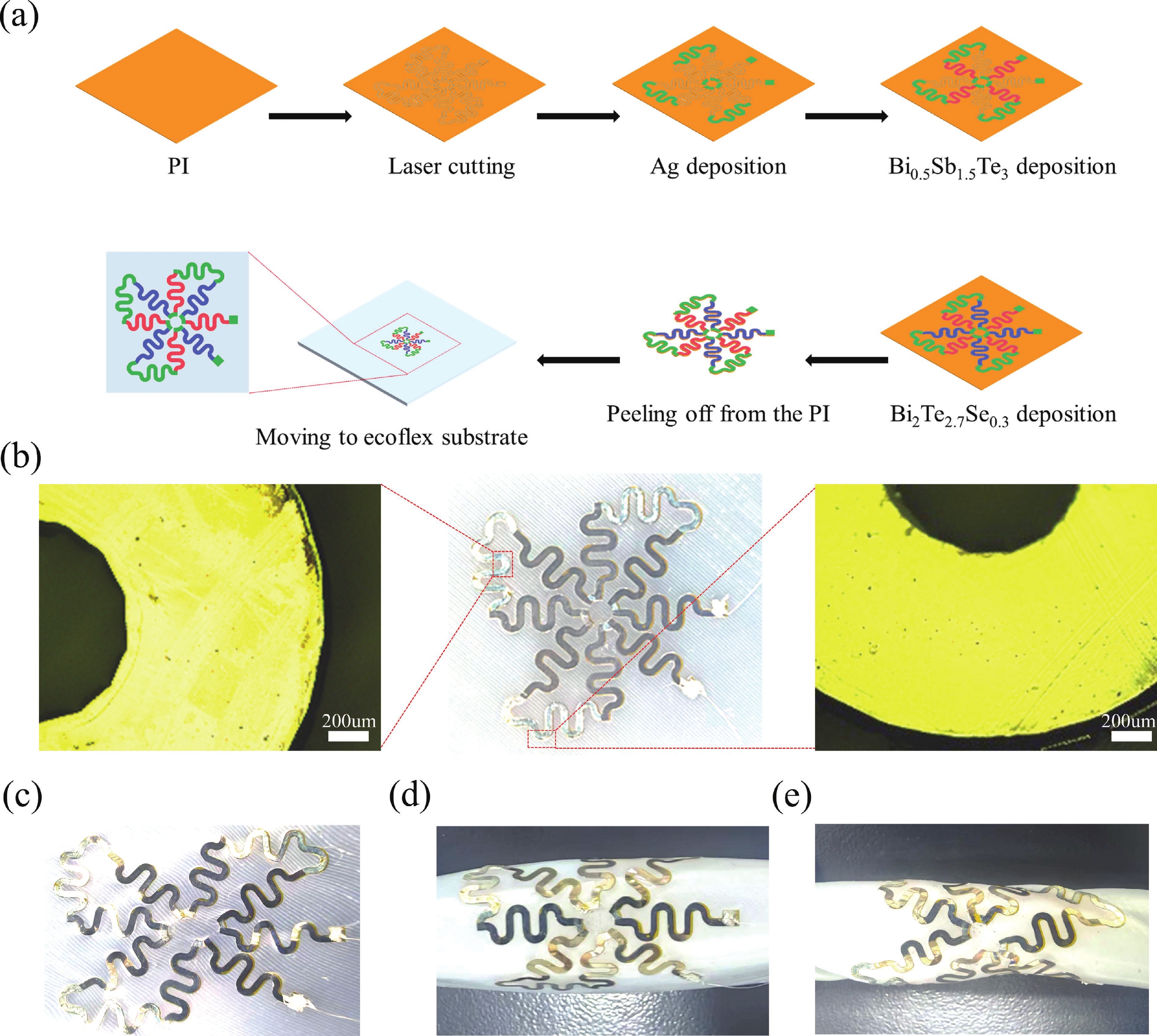
Thermoelectric power generation has attracted significant interest for its capability to directly convert thermal energy into electricity. Among various configurations, thin-film thermoelectric generators (TEGs) stand out due to their lightweight nature and facile integration, offering promising applications in waste heat recovery and wearable electronics. However, the performance of such devices under complex mechanical conditions, particularly under biaxial tensile strain, remains underexplored. In this work, we designed and fabricated a thin-film TEG insensitive to tensile strain and performed a parametric analysis using validated 3D numerical simulations to evaluate the effects of environmental conditions, material properties, and geometric parameters. Notably, the designed device maintained stable electrical performance under various biaxial tensile strains. Owing to its miniature and thin profile, variations in any component of the generator significantly affected its electrical performance. The results indicated that reduced thermal conductivity of the substrate and Ecoflex layer, as well as a thinner substrate, enhance the output voltage. Furthermore, longer thermoelectric legs within a certain range contributed to higher output voltage. Higher output voltage was more readily achieved when the inner radius length was close to the radius of the heat source. This work provides valuable insights for the development of high-performance compliant TEGs applicable in dynamic mechanical environments, such as complex stretching in the back and shoulder–elbow regions induced by human motion.
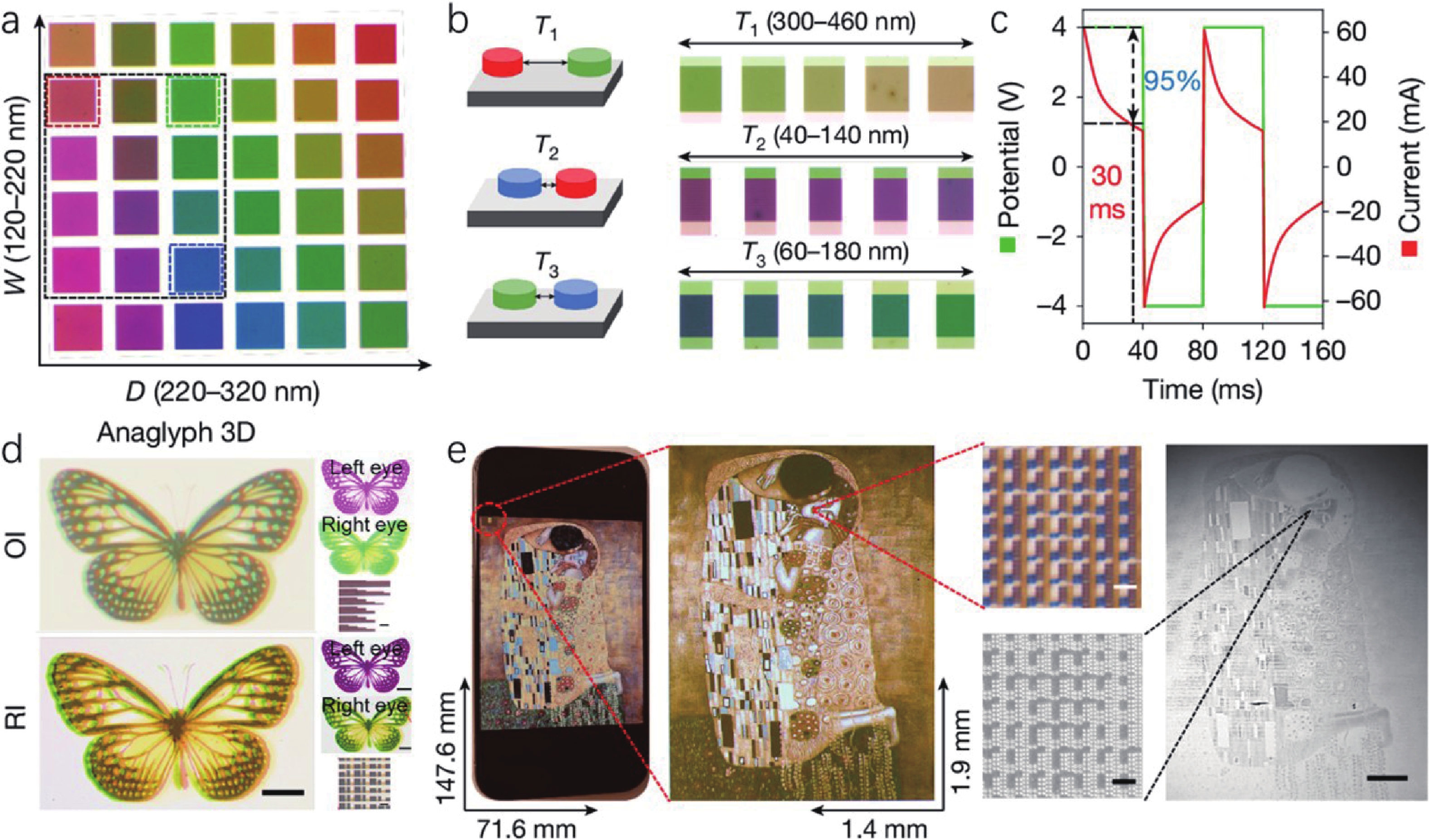

The introduction of high-k/metal gate (HK/MG) technology enables independent tuning of N-type metal−oxide−semiconductor (NMOS) and P-type metal−oxide−semiconductor (PMOS) threshold voltages, facilitating advanced nodes and improving overall chip performance. However, severe pattern loading effects during PMOS device fabrication pose challenges in dummy poly removal. This work reports the optimization of the photoresist etch back (PREB) process, providing a wider process window for subsequent AL CMP. By tuning the PR coating uniformity to 1.6% and applying four-zone electrostatic chuck (ESC) temperature control, the wafer-level uniformities of PR, SiN, and SiO2 were reduced to 6.3%, 2.3%, and 5.1%, respectively. An optimized over etch (OE) recipe with a high selectivity of PR : SiN : SiO2 ≈ 1 : 1 : 6 effectively balanced gate height loading between N- and PMOS regions. Furthermore, precise EB1 time tuning enabled defect removal, while advanced KLA inspection ensured early detection of critical failure modes. Collectively, these measures establish a robust and stable PREB process for advanced logic device fabrication.
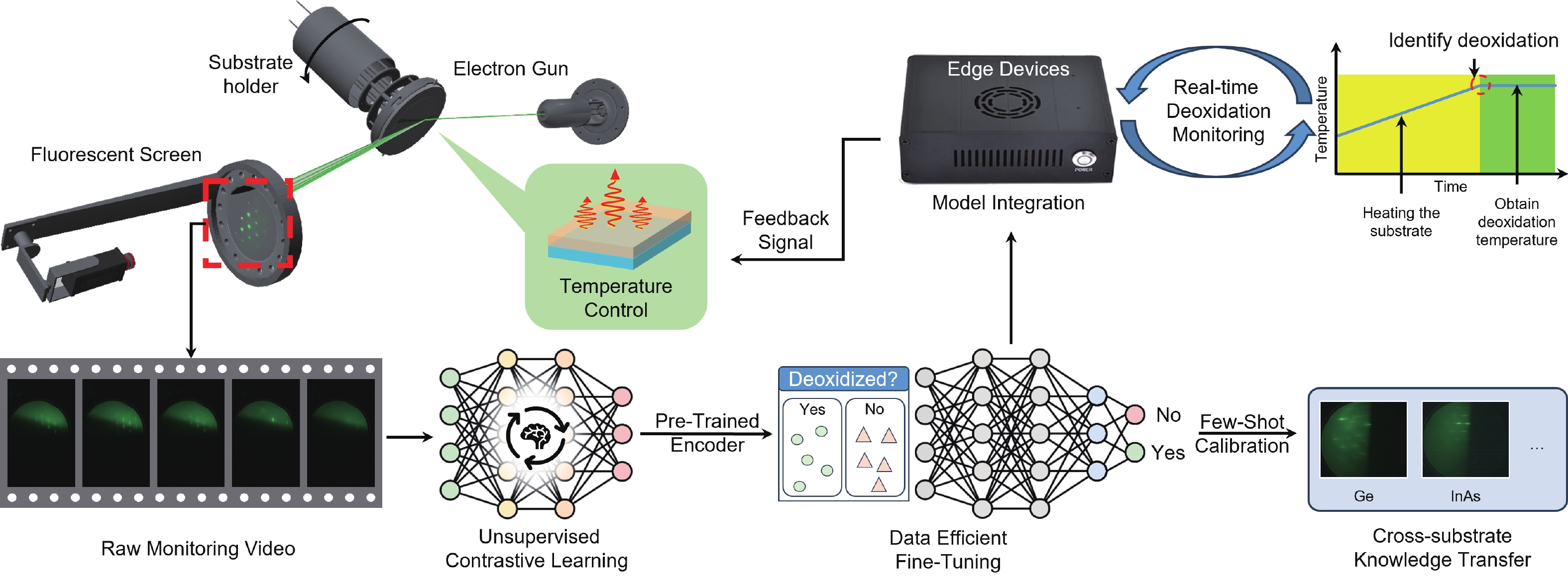
Accurate temperature control and effective oxide removal are essential for achieving high-quality epitaxial growth in molecular beam epitaxy (MBE). However, traditional methods often rely on manual identification of reflection high-energy electron diffraction (RHEED) patterns. This process is heavily influenced by the grower’s experience, leading to issues with reproducibility and limiting the potential for automation. In this report, we propose an unsupervised learning framework for real-time RHEED analysis during the deoxidation process. By incorporating temporal similarity constraints into contrastive learning, our model generates smooth and interpretable feature trajectories that illustrate transitions in the deoxidation state, thus eliminating the need for manual labeling. The model, pre-trained using grouped contrastive loss, shows significant improvement in RHEED feature boundary discrimination and localization of critical regions. We evaluated its generalizability through two transfer learning strategies: calibration-free clustering and few-shot fine-tuning. The pre-trained model achieved a clustering accuracy of 88.1% for GaAs deoxidation samples without additional labels and reached an accuracy of 94.3% to 95.5% after fine-tuning with just five sample pairs across GaAs, Ge, and InAs substrates. This framework is optimized for resource-constrained edge devices, allowing for real-time, plug-and-play integration with existing MBE systems and swift adaptation across various materials and equipment. This work paves the way for greater automation and improved reproducibility in semiconductor manufacturing.
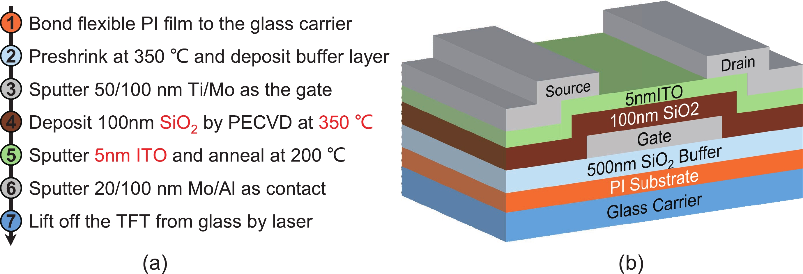
The increasing pursuit of ultra-high resolution displays has driven the demand for thin film transistors (TFTs) with higher mobility, especially on flexible substrates. In this work, we developed indium tin oxide (ITO) TFTs on flexible substrates for the first time and achieved a remarkable average mobility of 39.1 cm2·V−1·s−1, via mass-production compatible processes utilizing SiO2 gate dielectric. Benefiting from the ultra-flat surface and extremely low coefficient of thermal expansion (CTE) of our PI substrate, the ITO TFTs exhibit excellent large-scale uniformity. Additionally, the TFTs generate minor variations of −5.5% and +0.45 V in mobility and threshold voltage under a bending radius of 7 mm, respectively. They stay fully functional even after a dynamic bending test up to 13 000 cycles, observing no obvious degradation in mobility and threshold voltage. The reliable mechanical flexibility and robust bending durability demonstrate their great potential for ultra-high resolution flexible displays in the future.

The escalating need for high-performance artificial intelligence (AI) computing intensifies the "memory bottleneck" of the von Neumann architecture, prompting extensive exploration of computation-in-memory (CIM) solutions. This study is centered on the optimization of a high-efficiency, low-power "L"-shaped split-gate floating-gate (FG) memory for CIM applications. Fabricated on a 55 nm CMOS platform, the memory devices were systematically investigated through wafer acceptance test (WAT), Sentaurus™ simulations and comprehensive evaluations with the DNN + NeuroSim Framework V2.0. Among devices with diverse FG lengths, the 95-nm FG variant exhibits outstanding performance: it achieves a 5.35 V memory window, reaches a maximum conductance of 16.7 μS with excellent linearity under the varying voltage and width pulse scheme (VWPS), realizes 32-state multi-level storage, and attains a 92% training accuracy on the CIFAR-10 dataset using the VGG8 neural network.
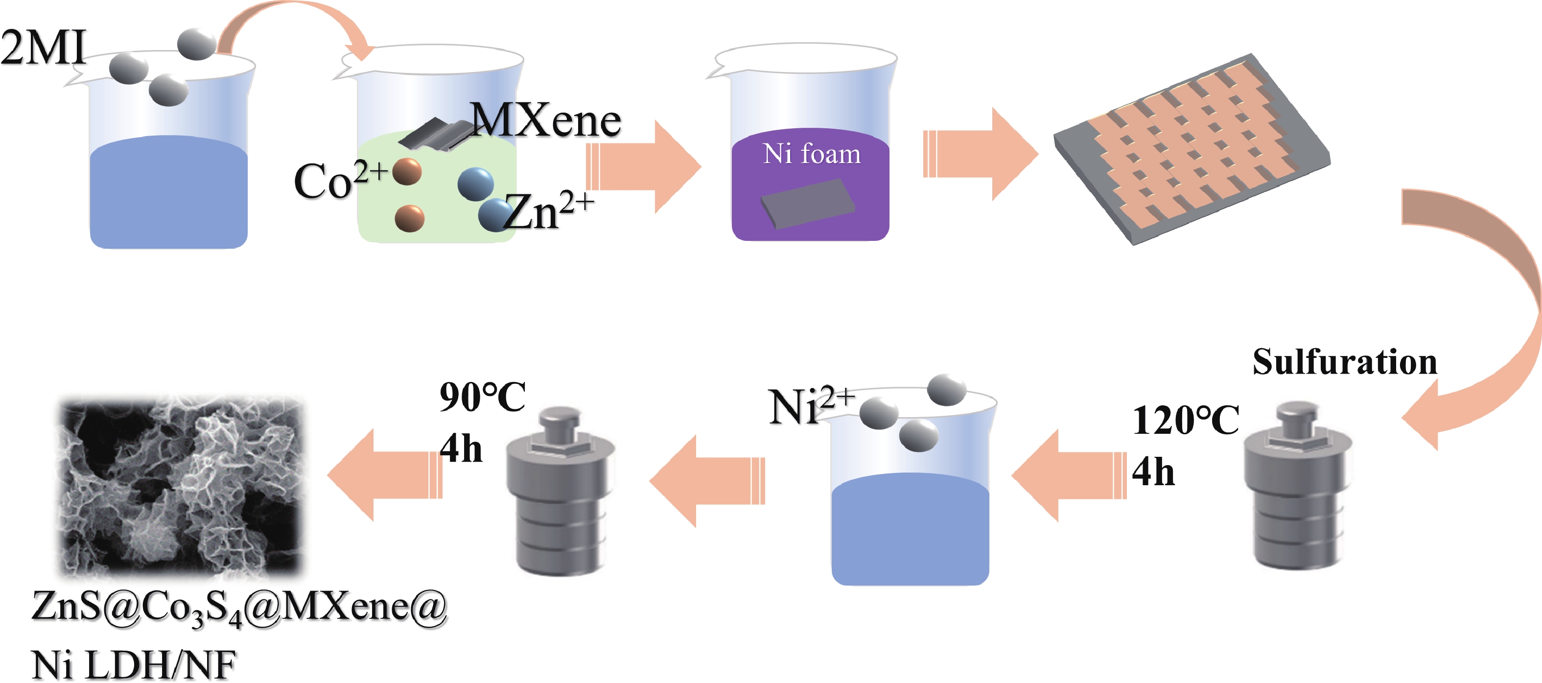
Zeolite imidazolate framework (ZIF)-derived bimetallic sulfides and layered double hydroxides (LDHs) have emerged as promising electrode materials for supercapacitors, owing to their porous layered structures, high electrochemical activity, tunable molecular architectures, low cost, and high specific capacitance. In this study, a unique composite material comprising ZIF-derived ZnCo bimetallic sulfide and LDH with a honeycomb-like structure was in situ grown on nickel foil (NF) via a controlled self-sacrificial template strategy. In contrast to previous reports, the resulting ZnS@Co3S4@MXene@Ni-LDH/NF composite integrates the advantages of MXene, LDH, and sulfides, leading to significantly enhanced conductivity, structural stability, and catalytic activity. The ZnS@Co3S4@MXene@Ni-LDH/NF electrode exhibits a uniform network structure with a thickness of approximately 1 µm coated on NF, and delivers a high specific capacitance of 1356.1 F·g−1 at a current density of 2 A·g−1. Furthermore, an asymmetric supercapacitor assembled with ZnS@Co3S4@MXene@Ni-LDH/NF as the positive electrode and activated carbon as the negative electrode achieves a high energy density of 34.08 Wh·kg−1 and a power density of 742.3 W·kg−1 at 1 A·g−1. This device successfully powers LED lights for 5 min, demonstrating its practical applicability. These results underscore the outstanding electrochemical performance of the ZnS@Co3S4@MXene@Ni-LDH/NF electrode, highlighting its potential for applications in supercapacitors and related energy storage fields.
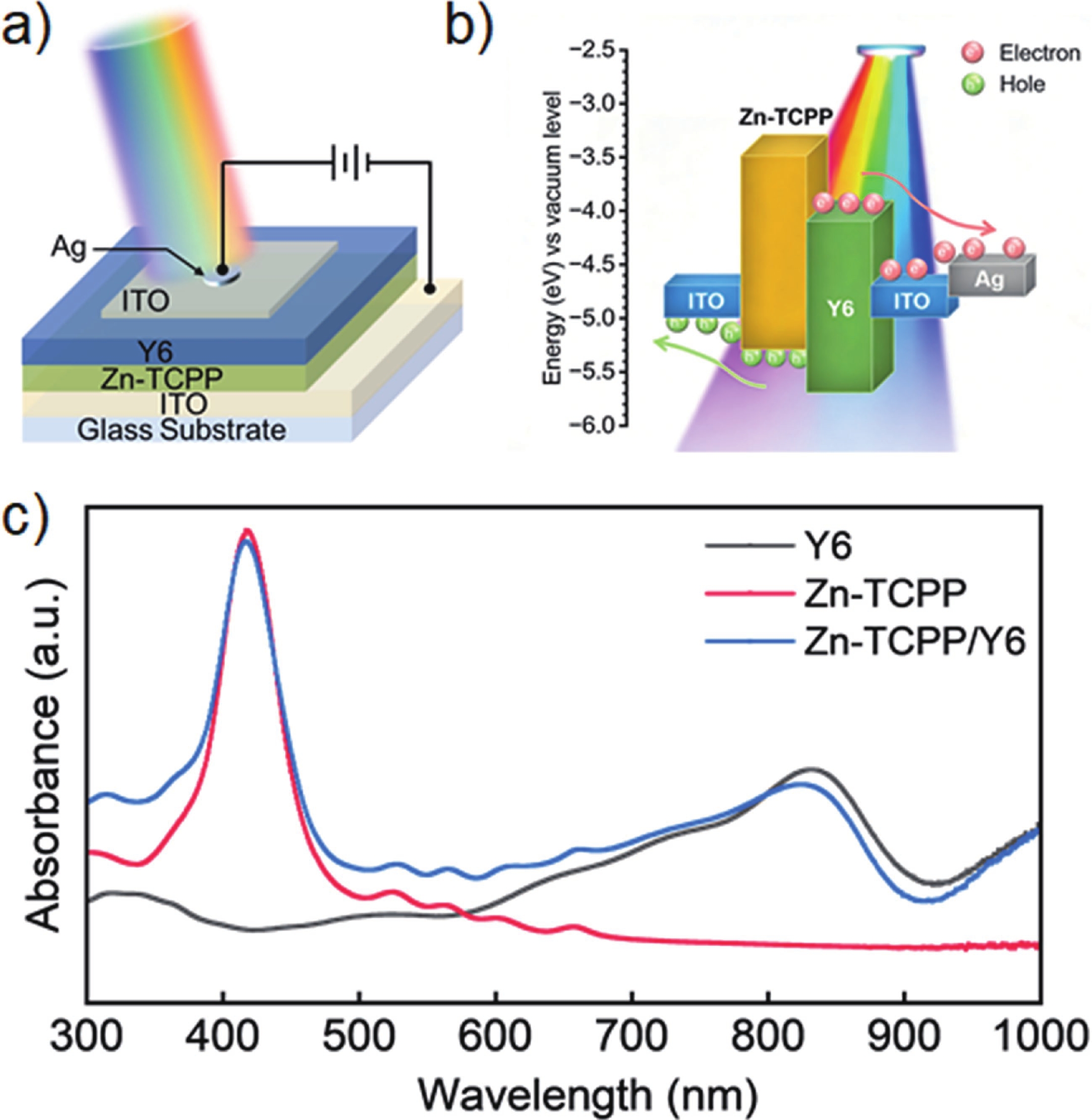
Broadband, low-power, and solution-processable organic photodetectors are essential for next-generation optoelectronic sensing. Two-dimensional conductive metal−organic frameworks (2D cMOFs) based on zinc tetracarboxyphenyl porphyrin (Zn-TCPP) offer strong light absorption and efficient charge transport, yet their photoresponse remains confined to the ultraviolet−visible (UV−Vis) region. To address this limitation, this study develops a solution-compatible strategy for constructing a well-defined MOF/organic semiconductor type-Ⅱ heterojunction by spin-coating a high-performance Y6 layer onto Zn-TCPP films. The resulting heterostructure provides complementary spectral absorption, promotes efficient exciton dissociation, and enables directional charge carrier transport, thereby achieving self-powered broadband photodetection spanning the ultraviolet to near-infrared (UV−NIR) range. The device demonstrates outstanding performance, including an ultra-low dark current (down to 3.40 × 10⁻¹³ A), high responsivity, and an ultrafast transient response with a rise time of 4.4 ms. This work establishes a generalizable approach for engineering high-efficiency MOF/organic semiconductor heterojunctions and offers a promising platform for low-cost, broadband, and self-powered photodetectors for biomedical and advanced sensing applications.
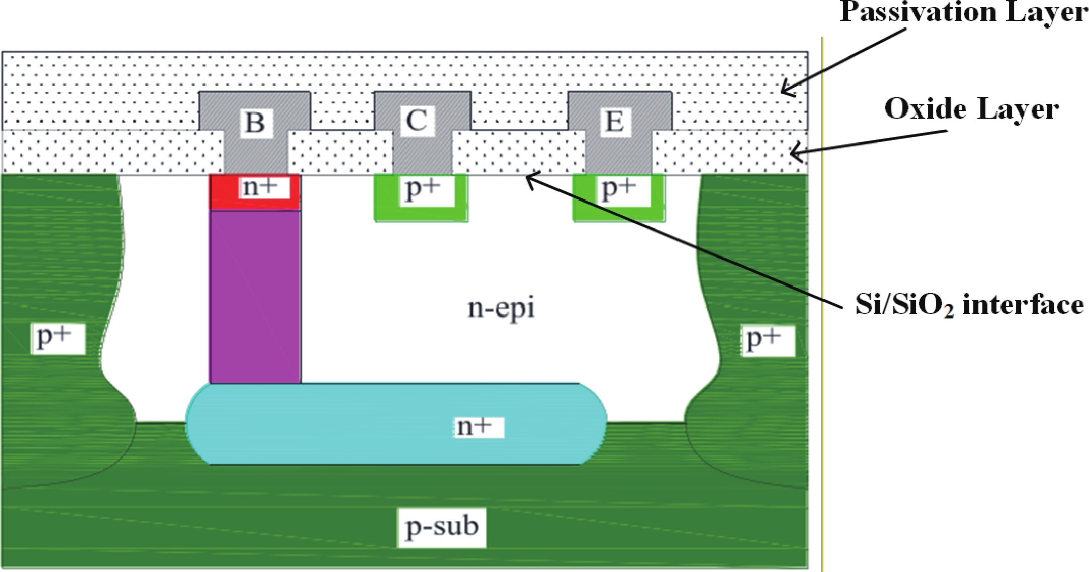
Enhanced low dose rate sensitivity (ELDRS) experiments were carried out on four commercial bipolar integrated circuits at dose rates ranging from 0.002 to 50 rad(Si)/s. Additionally, pre-irradiation elevated-temperature stress (PETS) experiments were conducted on the same devices at temperatures of 250 and 400 °C. The results show that for some devices, the radiation degradation when irradiated at an ultra-low dose rate of 0.002 rad(Si)/s is more than three times greater than that at a common low dose rate of 0.01 rad(Si)/s. Moreover, the maximum enhancement factor of the PETS effects reaches 20.3. It was also discovered that for devices exhibiting PETS effects, the saturation dose rate of ELDRS is less than 0.01 rad(Si)/s. A comprehensive analysis of the composition of the passivation layers indicated that the type and concentration of hydrogen bonds in these layers are the main factors contributing to the experimental outcomes.
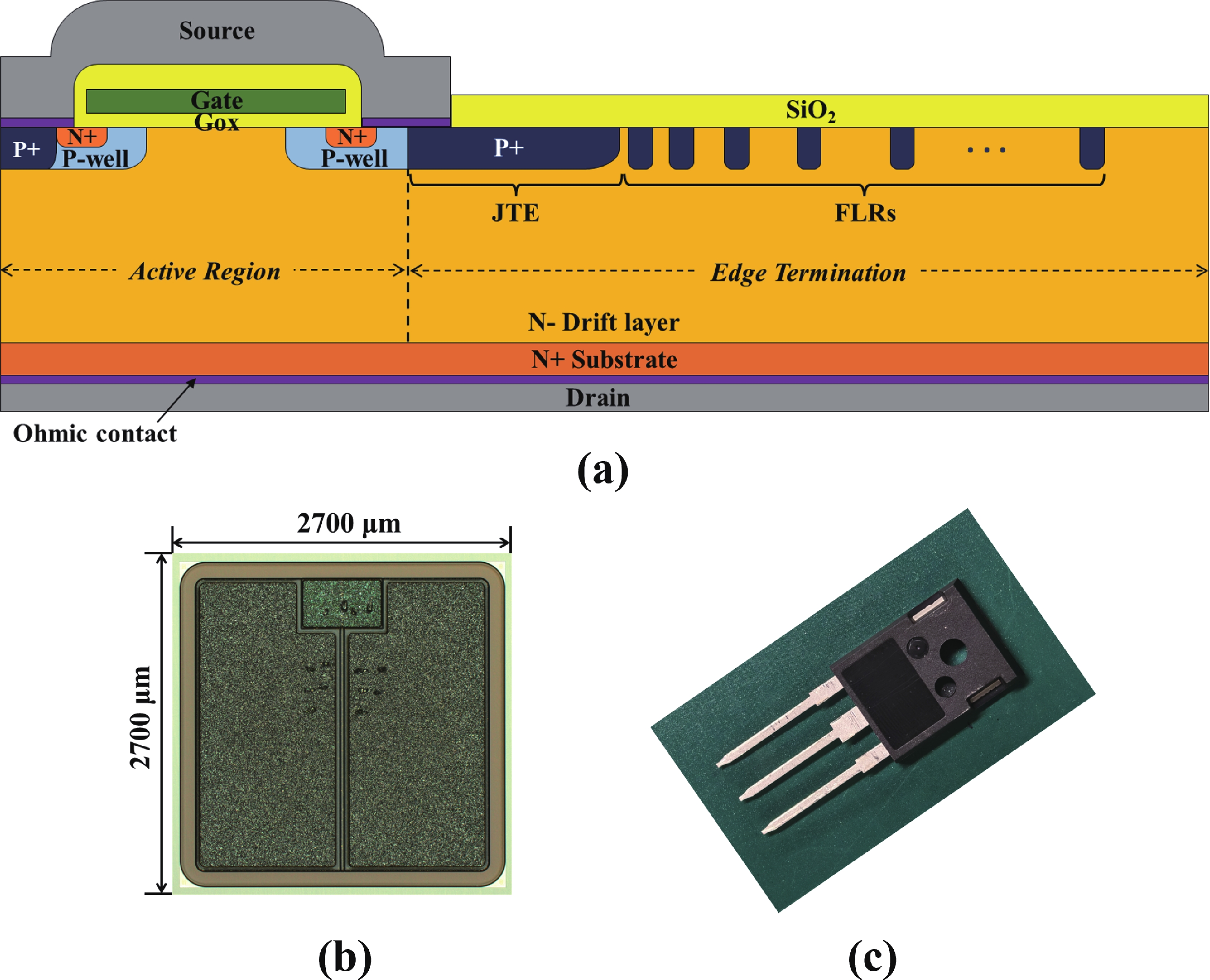
High-temperature reverse bias (HTRB) is one of the most critical reliability for SiC MOSFET, and the termination region is widely regarded as the sensitive area under HTRB stress. Interestingly, through systematically monitoring of the degradation behavior of static electrical parameters under different voltage, this study reveals that the elevated reverse bias (ERB) stress can also induce damage in the gate oxide, which results in the hole trapping and a negative shift of the threshold voltage. Deep level transient spectroscopy (DLTS) measurements were performed and showed that the interface trap density in the gate oxide is promoted after ERB stress. Surprisingly, the reverse leakage current after ERB stress is significantly deteriorated at a gate bias of 0 V, while effectively suppressed by applying a negative gate bias (−5 V), which point to the synergistic effects of channel region on the breakdown voltage. Based on the gate oxide degradations and TCAD simulations, it is elucidated that the trapped positive interface charges in gate oxide cause band bending, leading to the formation of an electron accumulation layer in the channel region at 0 V gate bias and thus resulting in a dominant leakage path. This work reveals the impact and mechanism of the ERB stress induced gate oxide damage on the breakdown voltage and highlights the importance of gate oxide protection, which is of great significance for improving the reliability of SiC MOSFETs in elevated voltage applications.
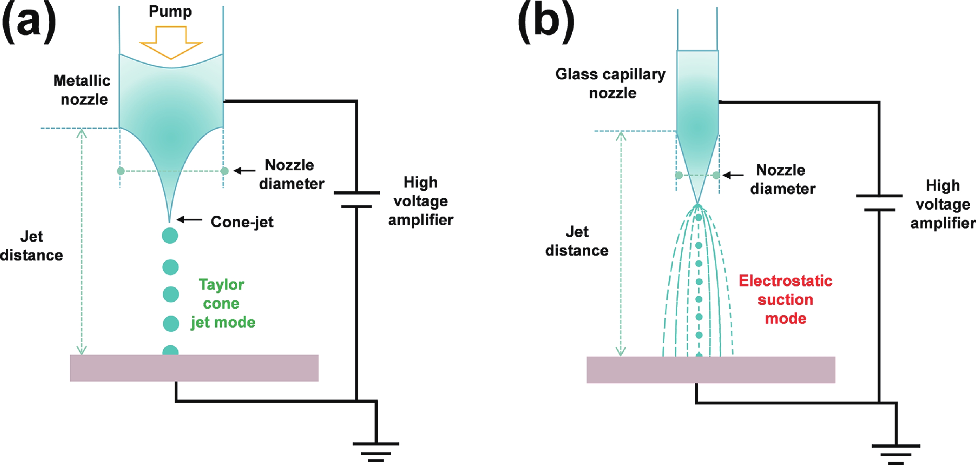
Electrohydrodynamic (EHD) inkjet printing has emerged as a powerful micro-/nanofabrication technique for high-resolution perovskite quantum dot (PeQD) color-conversion layers, offering precise control over pixel morphology, dimensions, and composition. This review systematically examines the mechanisms of cone-jet and electrostatic-attraction modes in EHD printing, highlighting recent advances in PeQD ink design, solvent and ligand engineering, and printing parameter optimization. Perovskite precursor and colloidal inks are discussed in detail, emphasizing strategies to enhance droplet ejection stability, suppress coffee-ring effects, and achieve uniform, high-luminescence pixels. Ligand exchange, dual-ligand passivation, and core−shell or polymer encapsulation are shown to effectively mitigate ion migration, surface defects, and environmental degradation, thereby improving photoluminescence efficiency and stability. Multi-channel and multi-nozzle EHD printing systems enable dynamic halide composition control and parallel RGB pixel deposition, facilitating ultrahigh-resolution patterning down to submicron feature sizes. Finally, the review highlights future directions, including synergistic PeQD material synthesis, advanced ink formulation, scalable high-throughput printing, and integration of PeQD color-conversion pixels into full-color micro-LED displays with minimal crosstalk and robust operational stability. These developments collectively demonstrate the immense potential of EHD inkjet printing for next-generation high-performance display technologies.

AlN/GaN high-electron-mobility transistor (HEMT) equipped with ultra-thin AlN barrier epitaxial structures were grown on 6-inch and 8-inch Si-based GaN templates via plasma-assisted molecular beam epitaxy (PAMBE). The AlN barrier thickness was systematically optimized to improve the properties of two-dimensional electron gas (2DEG). Structural and electrical characterizations were performed by atomic force microscopy (AFM), transmission electron microscopy (TEM), contact and non-contact Hall measurements. At an optimal AlN barrier thickness, an extremely low sheet resistance of 159.9 Ω/□ by contact Hall and 143.8 Ω/□ by non-contact Hall was achieved on the 6-inch HEMT wafer, marking a significant improvement over state-of-the-art Si-based GaN HEMTs. The epitaxial surface exhibited excellent morphology with a root-mean-square (RMS) roughness of 0.45 nm. Moreover, cross-sectional TEM analysis of PAMBE-grown AlN/GaN HEMT revealed an atomically sharp and structurally coherent heterointerface, whch is critical for achieving high electron mobility and reduced scattering loss. In addition, the 8-inch HEMT demonstrated a sheet resistance (Rs) as low as 115 Ω/□ by non-contact Hall with a uniformity is 2.13%, outperforming competing technologies than other companies on the market.
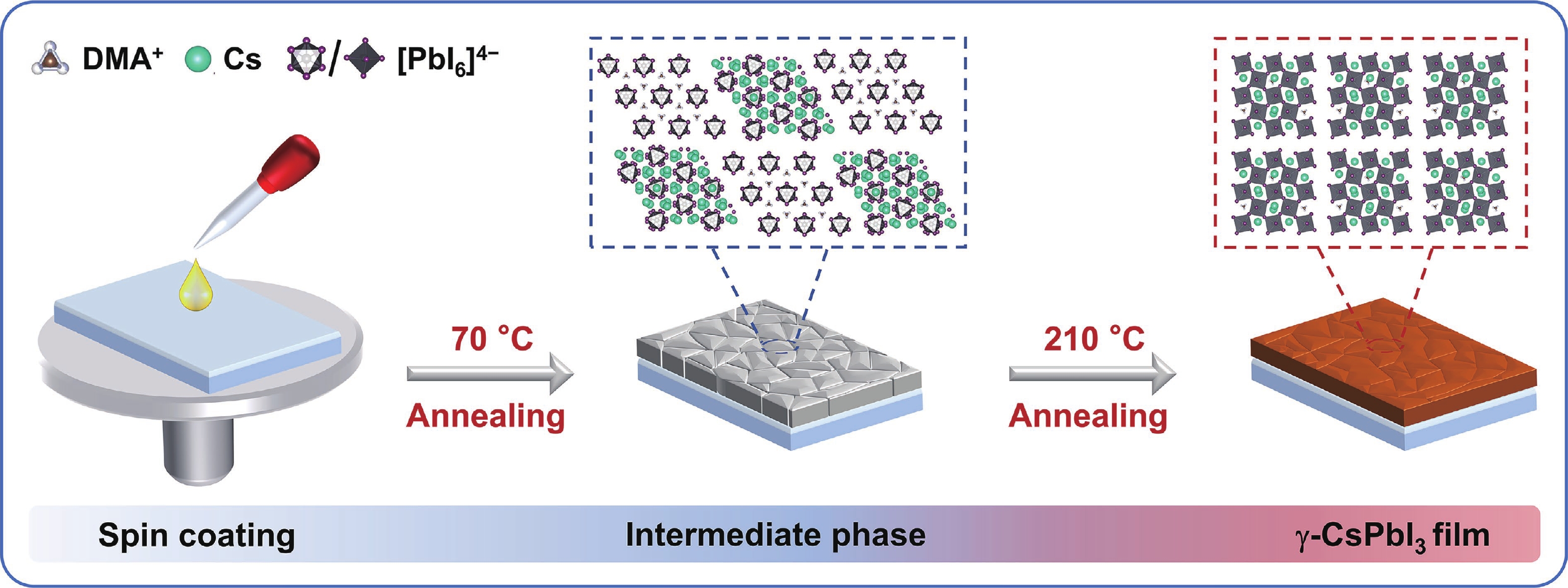
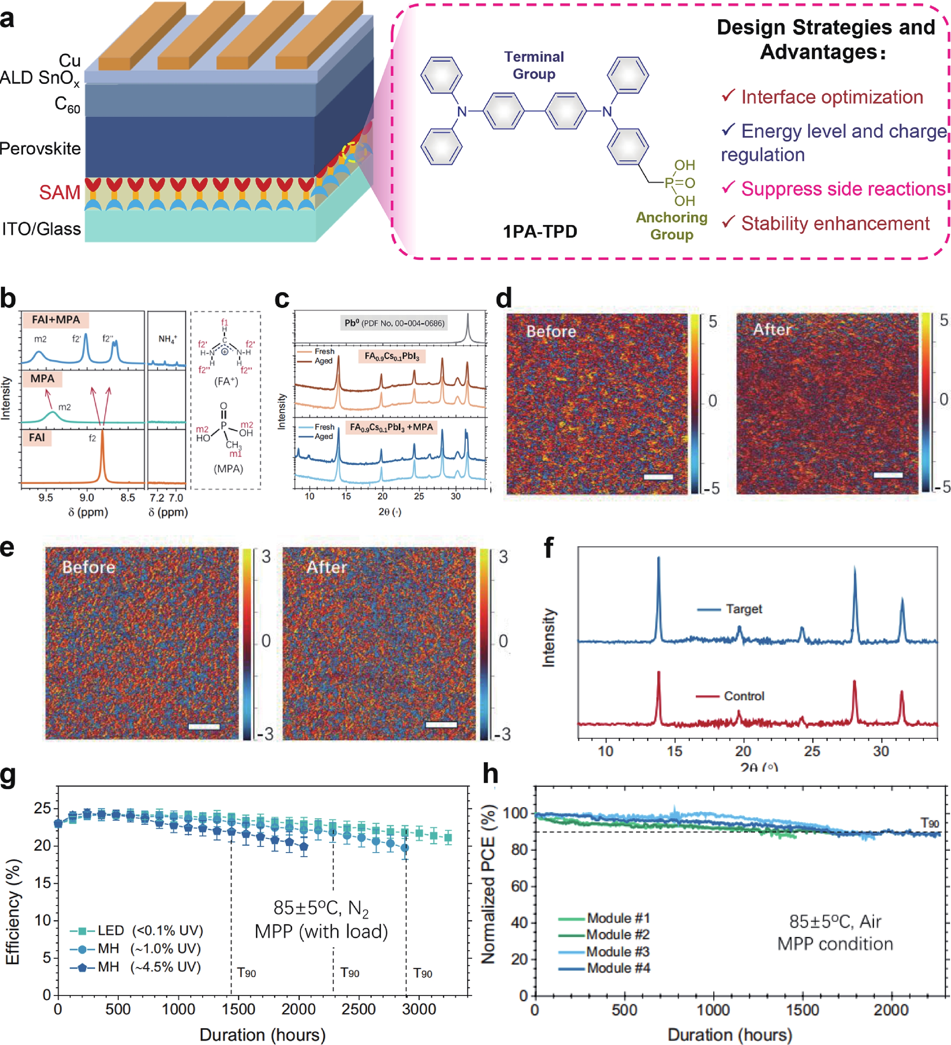
Inorganic cesium lead iodide (CsPbI3) perovskites are promising photovoltaic materials owing to their excellent thermal stability and optoelectronic properties. However, CsPbI3 film fabricated via solution processing typically suffers from high defect densities and detrimental residual tensile stress due to uncontrolled crystallization and thermal expansion mismatch with the substrate, which impedes its practical application. Herein, we introduce ammonium benzenesulfonate (ABS) as a bifunctional additive to modulate crystallization, thereby passivating defects and regulating residual stress. The sulfonate group of ABS coordinates with undercoordinated Pb2+ ions, while its ammonium group forms hydrogen bonds with iodide ions. The molecular structure of ABS bridges adjacent [PbI6]4− octahedra at grain boundaries. This dual interaction effectively enhanced crystallinity, suppressed non-radiative recombination, and improved structural stability. As a result, ABS-modified CsPbI3-based perovskite solar cells achieve an impressive power conversion efficiency (PCE) of 21.21% under standard illumination. Remarkably, they deliver a PCE of 40.85% under indoor lighting conditions. Moreover, unencapsulated devices retains 91% of their initial PCE after 800 h of storage in ambient air at a relative humidity of 5%.
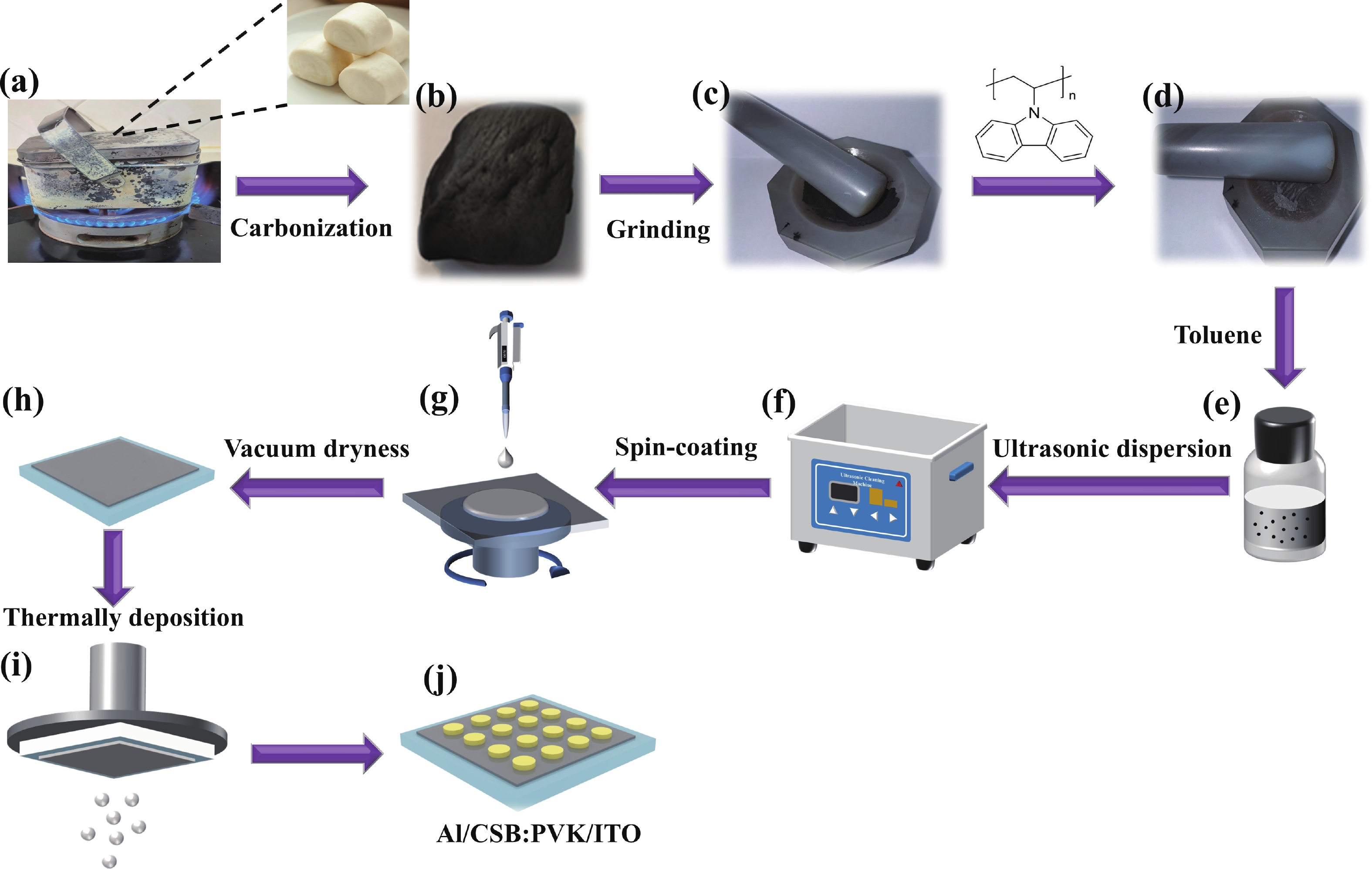
The development of new n-type semiconductors is crucial for the further advancement of electronic and optoelectronic devices. Steamed buns, anciently known as "man tou", mainly made of wheat flour and are one of the staple foods for Chinese people. After being subjected to high-temperature treatment, the steamed buns transformed into carbonized steamed buns (CSB) with porous nanostructures, which exhibit a Hall mobility of up to 1.62 cm2/(V·s), far greater than C60(1.5 × 10⁻³−2.5 × 10⁻² cm2/(V·s)), PCBM (2.0 × 10⁻⁷ cm2/(V·s)) and many polymer semiconductors (~10−6−10−2 cm2/(V·s)). A CSB-based bulk heterojunction memristor with a configuration of ITO/the CSB: PVK blends/Al is successfully fabricated. The device shows outstanding history dependent memristive switching performance, with 35 distinguishable conductance states, at a small sweep voltage range of ±1 V. An achieved production yield reaches up to 89%. Upon being subjected to consecutive positive or negative voltage sweeps, the current flowing through the device can be modulated continuously. When the 15 consecutive pulse voltages (pulse amplitude: 0.1 V; pulse width:10 μs, pulse period: 20 μs) were applied to the device, the observed total power consumption was about 7.63 nJ, suggesting a potential in low-energy neuromorphic computing applications. As expected, both the CSB and PVK do not exhibit any memristive effect under the same experimental condition. Utilizing the characteristic that the device can linearly adjust the weights, a simple convolutional neural network for traffic sign recognition was successfully constructed. After 300 rounds of training, the achieved recognition accuracy rate reached 88.77%. This work not only provides a new approach for developing low-cost and readily available organic semiconductors with high Hall mobility, but also offers a new idea for the subsequent development of high-performance artificial synapses and optoelectronic devices using carbonized steamed buns.
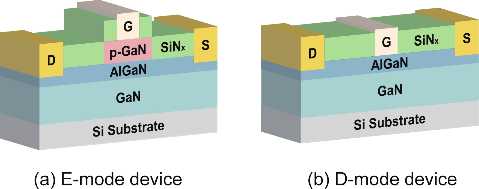
This paper demonstrates a monolithically integrated current reference and current mirror based on p-GaN gate HEMT technology, designed for high-temperature applications. The p-GaN current reference is composed of one D-mode and two E-mode devices. The generated reference current is independent of supply voltage since the proposed circuit incorporates a bias circuit capable of providing a supply-voltage-insensitive bias voltage. Moreover, under the zero-temperature coefficient (ZTC) bias voltage condition, the variation in the generated reference current at 200 °C is reduced by 15.4%, compared to a conventional p-GaN current reference with a bias voltage of 5 V. Experimental results indicate that the generated reference current slightly reduced from 2.53 to 1.70 mA over a broad temperature range of 25−200 °C. In addition, a current mirror circuit based on p-GaN HEMT technology was designed to imitate a reference current. The influence of temperature on the output current of the current mirror is mitigated, which could be realised by biasing the gate-to-source voltage at the zero-temperature coefficient voltage. This design sustains the current mirror mismatch error with small variation across a temperature range from room temperature to 200 °C. These results indicate that the GaN current reference and current mirror under zero-temperature coefficient bias voltage can ensure stable output current across different temperatures, facilitating the application of fully GaN integrated circuits in high-temperature environments.
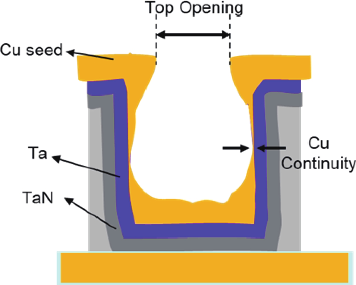
The downscaling of logic devices has posed numerous engineering and manufacturing challenges in copper (Cu) interconnections. The primary failure modes of Cu filling defects are narrow top openings and discontinuous Cu seeds on sidewalls. This study investigates the influence and mechanism of layout on Cu filling defects. Dense line wires with uneven local layouts are prone to defects, which is attributed to the altered distribution of additives in electrochemical plating (ECP), leading to differences in bottom-up filling behavior. It is demonstrated that large-sized metal conductor regions adjacent to dense line wires adsorb substantial amounts of suppressor, resulting in sparse current density in these areas. Given the fixed total local current density, the sparseness of current density in adjacent regions inevitably diverts more current lines to the dense line wire areas. The excessive current density exceeds the local redistribution capacity of additives, causing premature sealing of trench tops and the formation of void defects. A low-current plating process significantly mitigates these defects but may compromise the protective capability of the Cu seed. Additionally, the perimeter density of the layout serves as an effective evaluation index.
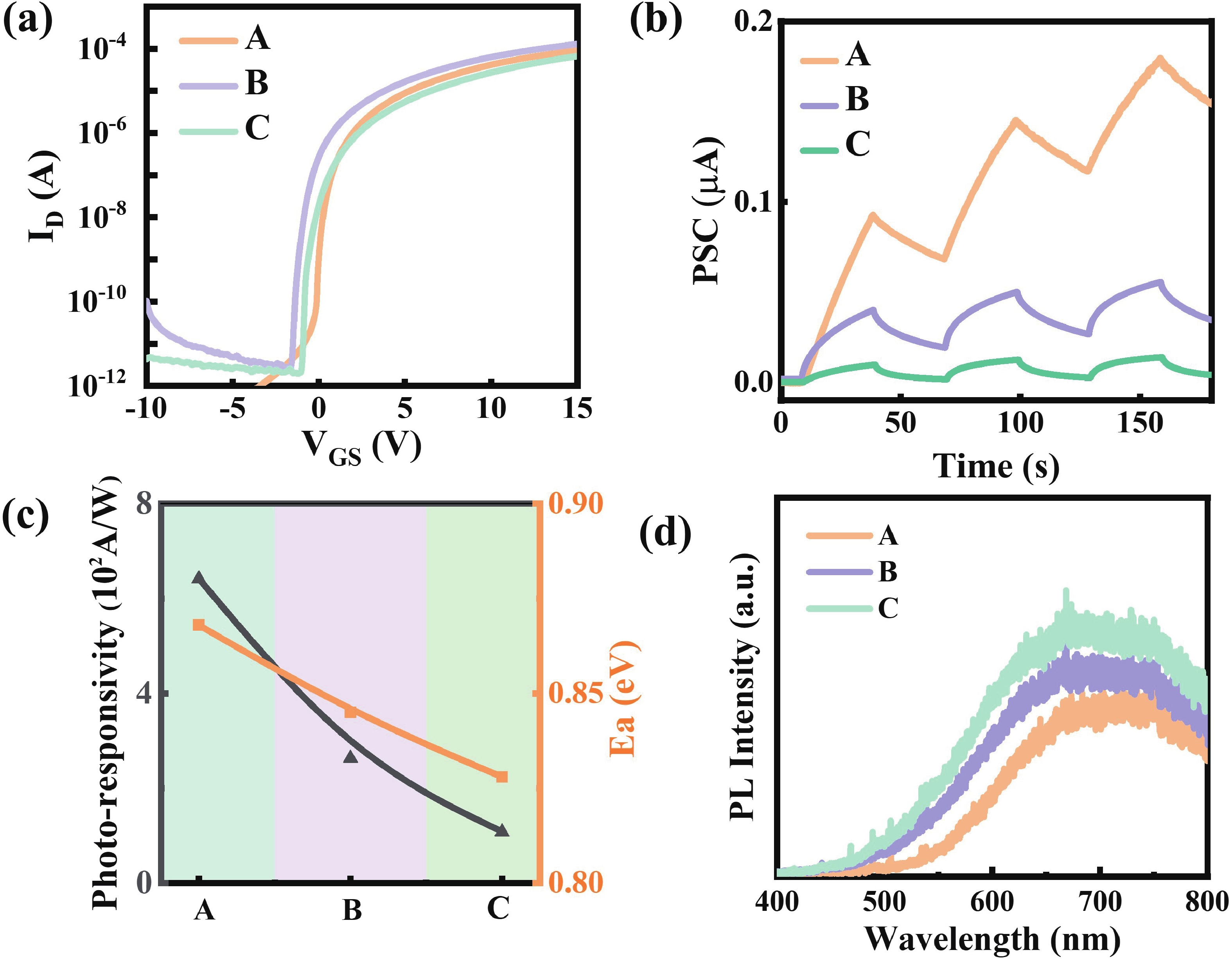
Oxide semiconductor-based neuromorphic devices hold great potential for visual information processing, yet their performance is critically limited by photolithography-induced organic residues. This work systematically investigates the effects of photoresist contaminants on In−Ga−Zn−O thin-film transistors (IGZO TFTs), revealing that these residues introduce deep-level trap states that degrade both photo-responsivity and carrier transport dynamics. Through optimized plasma-assisted surface treatments, these adverse effects would be effectively eliminated. Additionally, we show that gate−voltage modulation can precisely control the relaxation kinetics of photocarriers in these devices. By applying these strategies to IGZO-based synaptic arrays, we achieve enhanced image contrast through controlled optoelectronic response modulation. Overall, our findings highlight the critical impact of photolithography-induced organic residues in IGZO optoelectronic synaptic devices and demonstrate an effective approach for performance enhancement through surface plasma treatment and gate−voltage modulation.
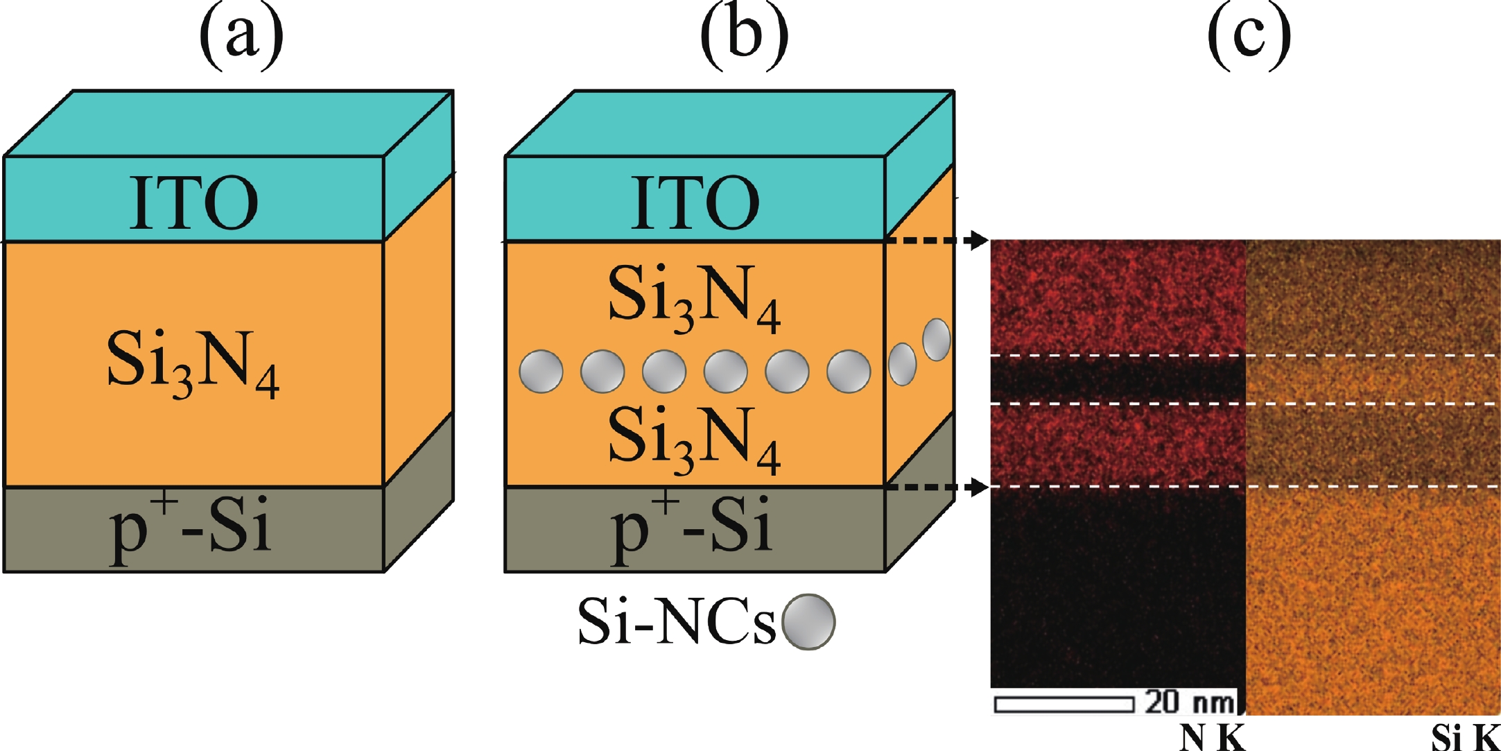
This work focuses on the study of the resistive switching (RS) properties of metal−insulator−semiconductor (MIS)-like structures based on silicon nitride (Si3N4) and Si3N4 with embedded silicon nanocrystals (Si-NCs) as the switching layer for the development of memristor devices. The formation of Si-NCs in the Si3N4 matrix, along with its chemical composition, was confirmed by Raman, transmission electron microscope (TEM), and energy-dispersive X-ray spectroscopy (EDS) analyses. The introduction of Si-NCs within the Si3N4 improved the performance of the devices. For Si3N4-based memristor devices, SET and RESET voltages of 2.38 and −1.38 V were obtained, respectively, while these values were reduced to 0.36 V (SET) and −0.11 V (RESET) for Si3N4:Si-NCs-based RS devices. Both RS devices exhibit at least 180 RS cycles, but with an increased ON/OFF ratio from 103 (Si3N4) to 106 when Si-NCs are embedded. The retention time analysis shows that the low resistance state (LRS) and the high resistance state (HRS) are stable for up to 104 s. The analysis of the conduction mechanism indicates that HRS is driven by the space-charge-limited conduction (SCLC), and the LRS by an Ohmic conduction mechanism. A model of the RS mechanism was proposed to understand the role of Si-NCs in the dielectric matrix.

Solar-blind ultraviolet photodetectors (UV PDs), capable of detecting UV radiation without interference from sunlight, have attracted significant interest. Herein, we propose a 0D/1D heterostructure for UV PDs, which was fabricated by spin-coating MoS2 quantum dots onto p-AlGaN nanowires. The device achieves a high responsivity of 175.5 mA/W and a fast response speed of 83 ms at 250 nm illumination under self-powered mode, which improved nearly 1235% and 521% after MoS2 decoration, respectively. These improvements can be attributed to the type-Ⅱ heterostructure formed between p-AlGaN and MoS2, which facilitates enhanced charge separation and carrier transport. Later, we demonstrate the implementation of this device in optical communication, achieving high-accuracy transmission of "GaN" ASCII code signals. Such a 0D/1D heterostructure provides an effective strategy for high-performance solar-blind UV PD.
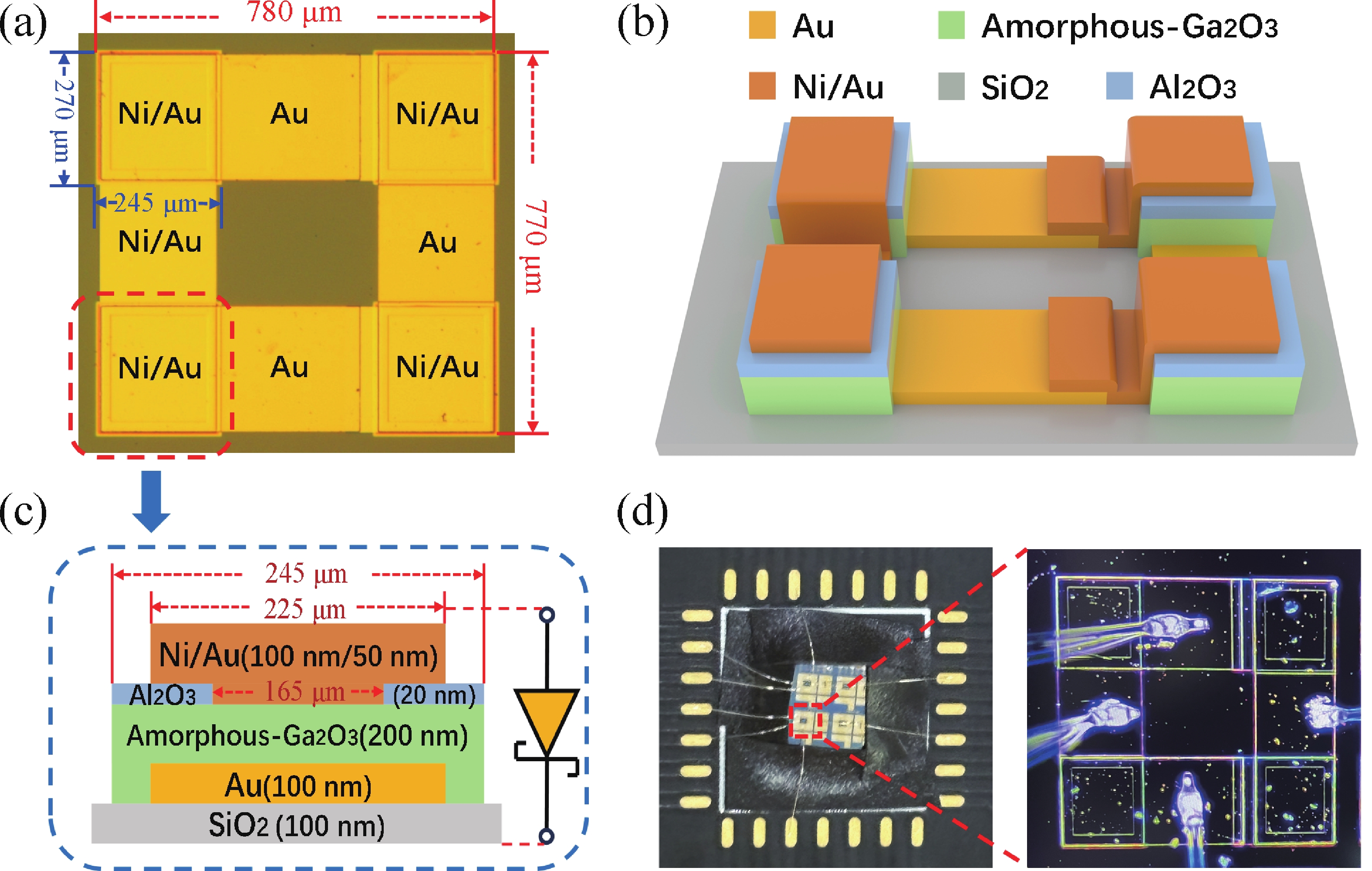
This paper demonstrated a monolithically integrated 200 nm-ultrathin amorphous-Ga2O3 vertical SBD-based bridge rectifier and its hybrid buck conversion system with a Si-MOSFET. The fabricated vertical Ga2O3 SBD exhibits excellent characteristics and a high breakdown electric field strength of 1.35 MV/cm. The bridge rectifier circuit maintains stable operation at high frequencies of 50 kHz. And the hybrid buck system composed of the Ga2O3 bridge rectifier and Si-MOSFET achieves adjustable step-down voltage output under the conditions of a 20 kHz switching frequency of Si-MOSFET and 50 Hz Vin. This work validates the practical value of Ga2O3 rectifiers in high-frequency conversion systems.
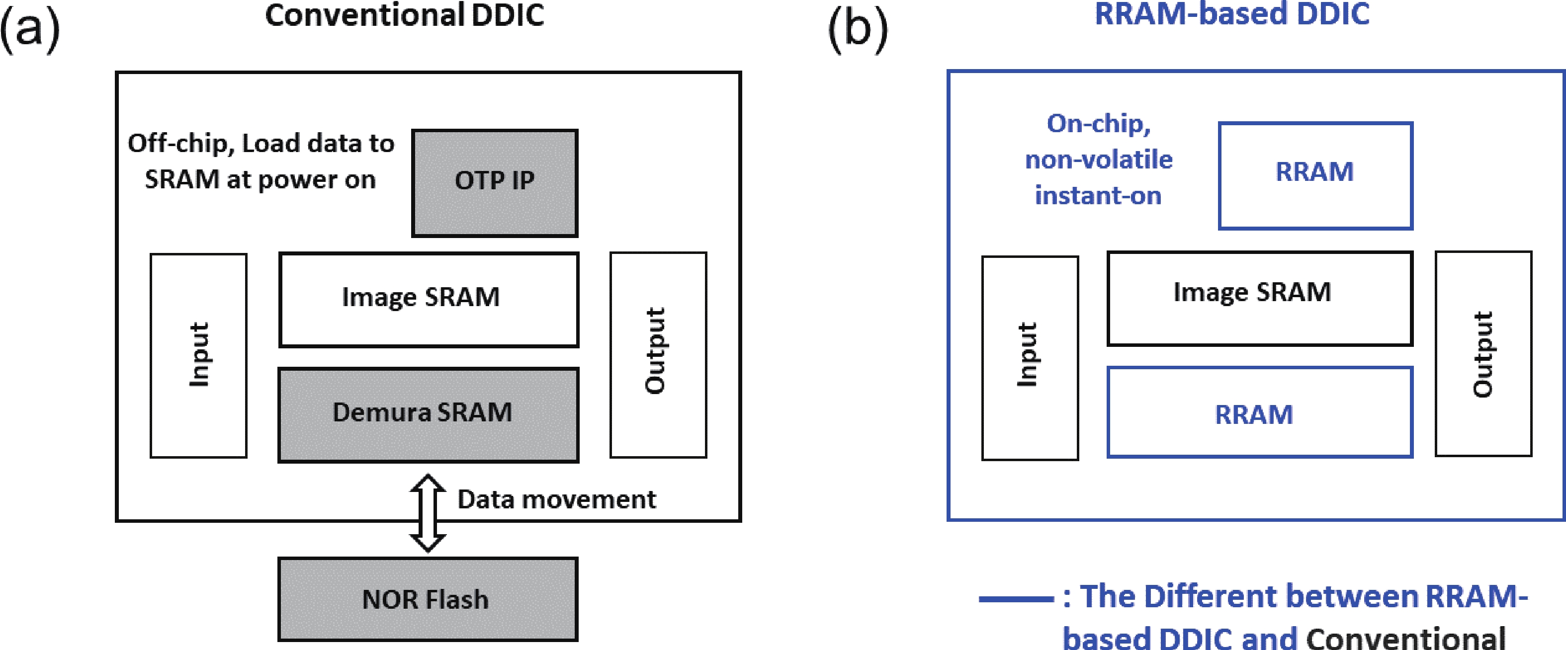
To address the challenges of complexity, power consumption, and cost constraints in traditional display driver integrated circuits (DDICs) caused by external NOR Flash and SRAM, this work proposes an embedded resistive random-access memory (RRAM) integration solution based on a 40 nm high-voltage CMOS logic platform. Targeting the yield fluctuations and stability challenges during RRAM mass production, systematic process optimizations are implemented to achieve synergistic improvements in RRAM performance and yield. Through modifications to the film sputtering and pre-deposition treatment, the within-wafer resistance uniformity (RSU) of the oxygen-deficient layer (ODL) thin film is improved from 11% to 8%, while inter-wafer process stability variation reduces from 23% to below 6%. Consequently, the yield of 8 Mb RRAM embedded mass production products increases from 87% to 98.5%. In terms of device performance, the RRAM demonstrates a fast 4.8 ns read speed, exceptional read disturb immunity of 3 × 10⁸ cycles at 95 °C, 103 write/erase endurance cycles for the 1 Mb cells, and data retention of 12.5 years at 125 °C. Post high-temperature operating life (HTOL) testing exhibits stable high/low resistance window. This study provides process optimization strategies and a reliability assurance framework for the mass production of highly integrated, low-power embedded RRAM display driver IC.
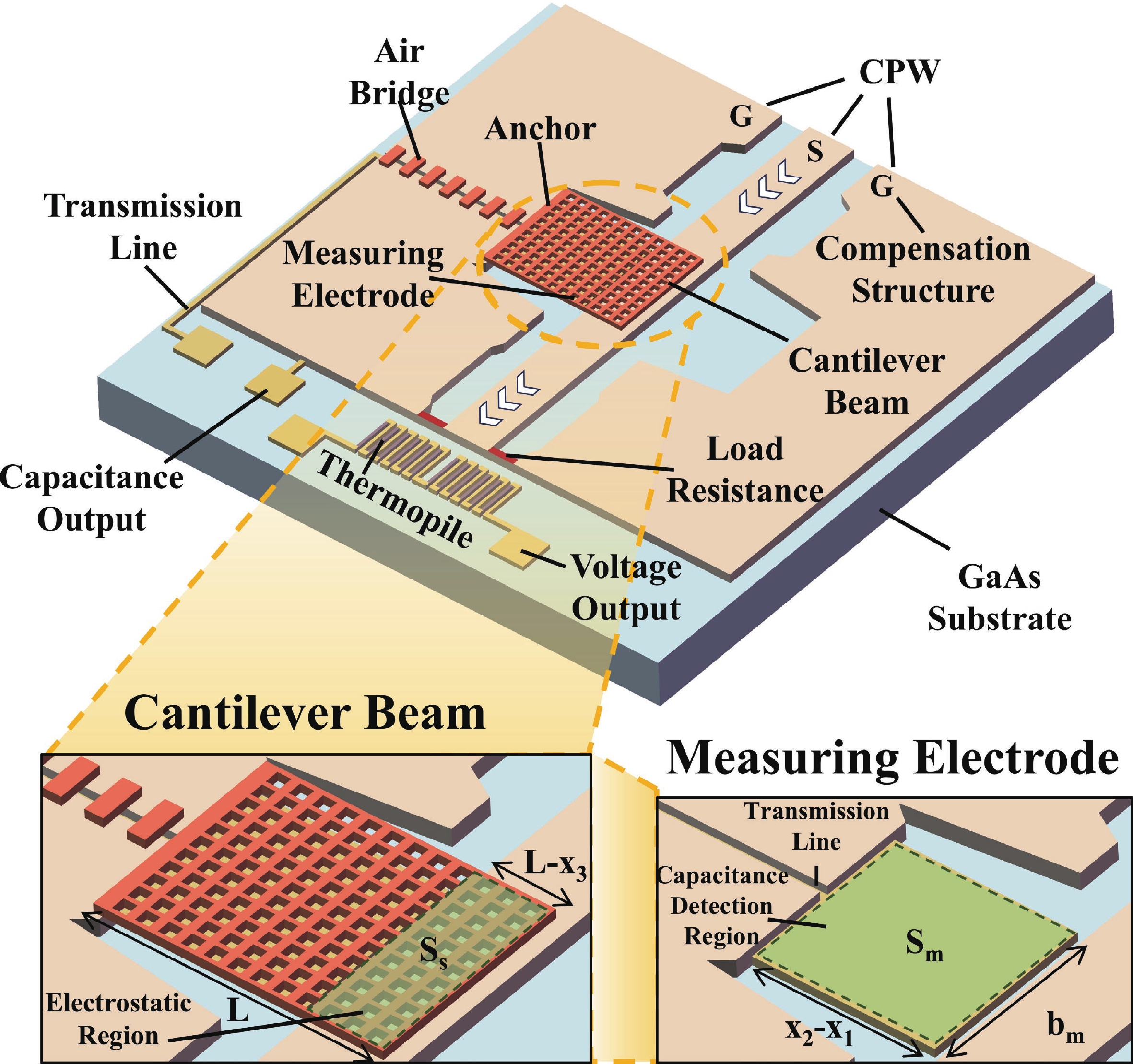
To improve the theoretical prediction accuracy of static mechanical quantities in MEMS cantilever beams for microwave power detection chips, a distributed static model is proposed based on the deflection equation. An analytical framework is established through the precise characterization of cantilever beam bending. The framework can accurately extract key electromechanical parameters, and the correlation between these parameters and geometric changes is systematically studied. Results show that the pull-in voltage increases with the gap but decreases with the length. The predicted pull-in voltage indicates a relative error of only 6.5% between the distributed static model and the simulation, which is significantly lower than that of the other two models. The overload power and sensitivity are also analyzed to facilitate performance trade-offs in chip design. The measured return loss varies between −66.46 and −10.56 dB over the 8−12 GHz frequency band, exhibiting a characteristic V-shaped trend. Moreover, the measured sensitivity of 66.5 fF/W closely matches the theoretical value of 69.3 fF/W, showing a relative error of 5.6%. These findings confirm that the distributed model outperforms the other two in terms of both accuracy and physical realism, thereby providing important reference for the design of microwave power detection chips.
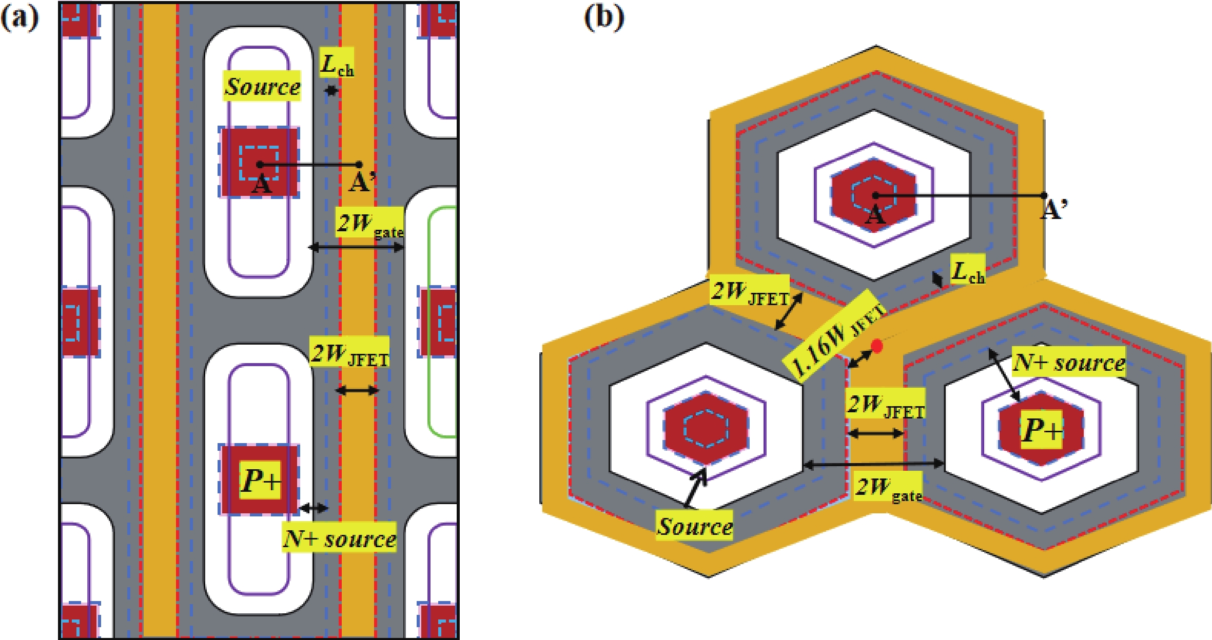
High gate oxide electric field, which can lead to device failure, is a common issue in SiC MOSFETs. To mitigate this issue and ensure high device reliability, an electric field shielding layer (also called depletion layer) in JFET region is always used to reduce the gate oxide electric filed strength (Eox,max). However, there is still a lack of a detection methods to characterize the changes in the depletion layer of the JFET region. In this paper, a type of 1200 V 4H-SiC MOSFET with different JFET widths and cell topologies is designed and fabricated, and an innovative detection method for the depletion layer of JFET region is proposed for the first time. This method is adopted to focus on discussing the influence of the depletion layer formed by different JFET widths on Vg, and the changes in the gate oxide capacitance Cg of hexagonal cells and linear cells during the formation of the JFET depletion layer are studied. Finally, the robustness of different cell topologies and JFET widths is determined by the depletion voltage drift in the high temperature gate reverse bias tests (HTGB−) reliability test.

Spin-transfer-torque magnetic random-access memory (STT-MRAM), based on magnetic tunnel junctions (MTJs), is attracting significant attention for applications demanding high reliability and speed. To ensure high TMR which is essential for achieving sufficient sense margin, MTJs typically incorporate relatively thick tunnel barriers, resulting in high operating voltages. As the CMOS technology nodes advance and operating voltages decrease, reducing the MTJ switching voltage becomes imperative. However, MTJs with thinner tunnel barriers generally exhibit significantly degraded read margins and bit error rate, presenting a major challenge for achieving high-density, low-power MRAM. Here, we address this challenge through MgO tunnel barrier engineering and process optimization, successfully reducing the required MOS driving voltage while simultaneously expanding the write margin. Meanwhile, 85% array yield with sub-parts-per-million bit error rates at RA = 7 Ω·μm2 is achieved. These advancements are promising for developing high-density MRAM at advanced technology nodes.
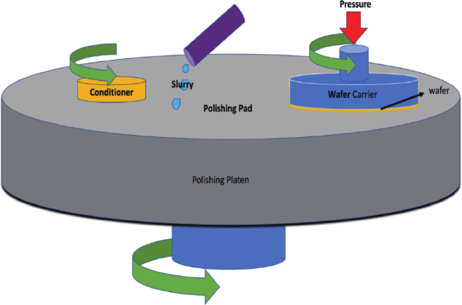
Chemical mechanical polishing (CMP) serves as an indispensable process for achieving global planarization in semiconductor manufacturing, especially as integrated circuit (IC) technology advances to sub-7 nm nodes, where atomic-level surface flatness becomes crucial. Silica abrasives, which account for over 90% of the abrasive market in advanced CMP processes, operate not through simple mechanical grinding but through a key "chemical-mechanical synergistic" mechanism: chemically softening the wafer surface, then mechanically removing the softened layer to expose a new surface, which is further softened and removed, repeating this cycle to produce a smooth wafer. Despite their prevalence, conventional silica abrasives still face challenges, including relatively low material removal rate (MRR), a tendency to agglomerate, leading to poor dispersion and surface defects, and limitations in achieving ultimate surface uniformity. Significant progress has been made to address these issues. Development has progressed from simple spherical particles to complex structural designs (such as mesoporous, hollow, and raspberry-shaped structures) to enhance slurry transport and mechanical action. Surface chemical modifications (e.g., using amino or polymer groups) can improve dispersion stability and reduce scratching. Furthermore, composites with other materials (e.g., ceria, polymers) and precise control of particle size distribution are key to enhancing performance. These innovative approaches have yielded significant performance gains. State-of-the-art slurries have demonstrated the ability to achieve surface roughness below 0.1 nm rms. The development of silica abrasives is increasingly focused on sustainability and smart manufacturing. A prominent direction is the design of biodegradable abrasives that disintegrate after use, thereby simplifying post-chemical mechanical polishing (CMP) cleanup and minimizing environmental impact—an approach fully aligned with green manufacturing principles. This review systematically summarizes the progress of silica abrasives for CMP over the past 60 years. This summary provides theoretical insights and forward-looking strategies to overcome the current limitations of abrasive technology. We believe this review will be helpful in advancing the field of CMP abrasives towards next-generation semiconductor manufacturing.
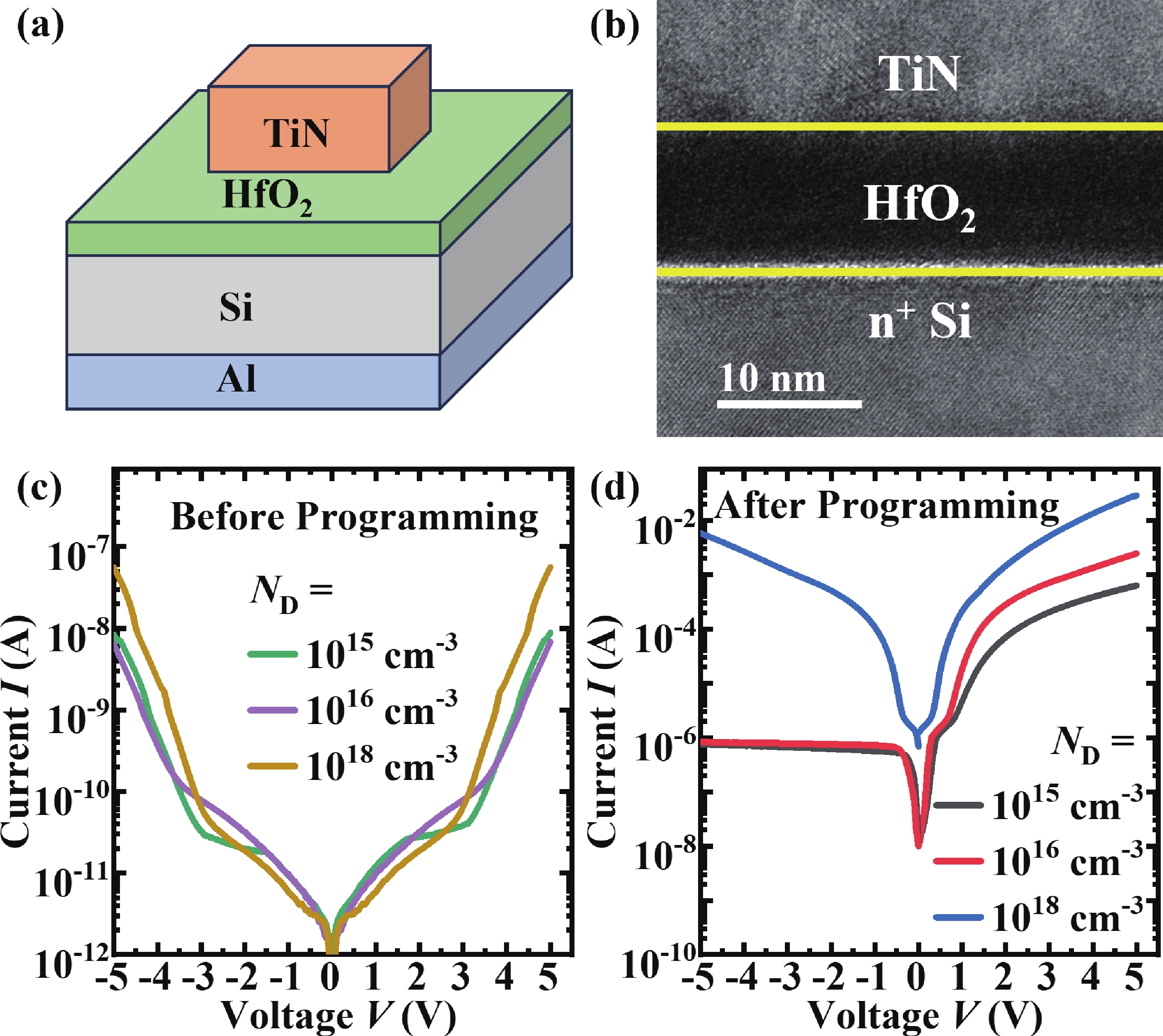
In this work, the oxide-based programmable diodes (PDs) with structure of TiN/HfO2/Si/Al are fabricated, and its electron transport mechanisms are investigated. Electrical measurements results depicted that the conduction and rectification performance of oxide-based PDs are mainly controlled by the interface between oxygen vacancies (VOs) consisted filament and semiconductor electrode. The local density of state in filament and band-bending of the PDs are calculated by first-principal simulation. The electron transport in oxide PDs is dominated by Poole−Frenkel emission under forward bias, while under negative bias, the PDs behave like a reverse Schottky-diode. These mechanisms research is necessary for device optimization and circuit design of oxide-based PDs.
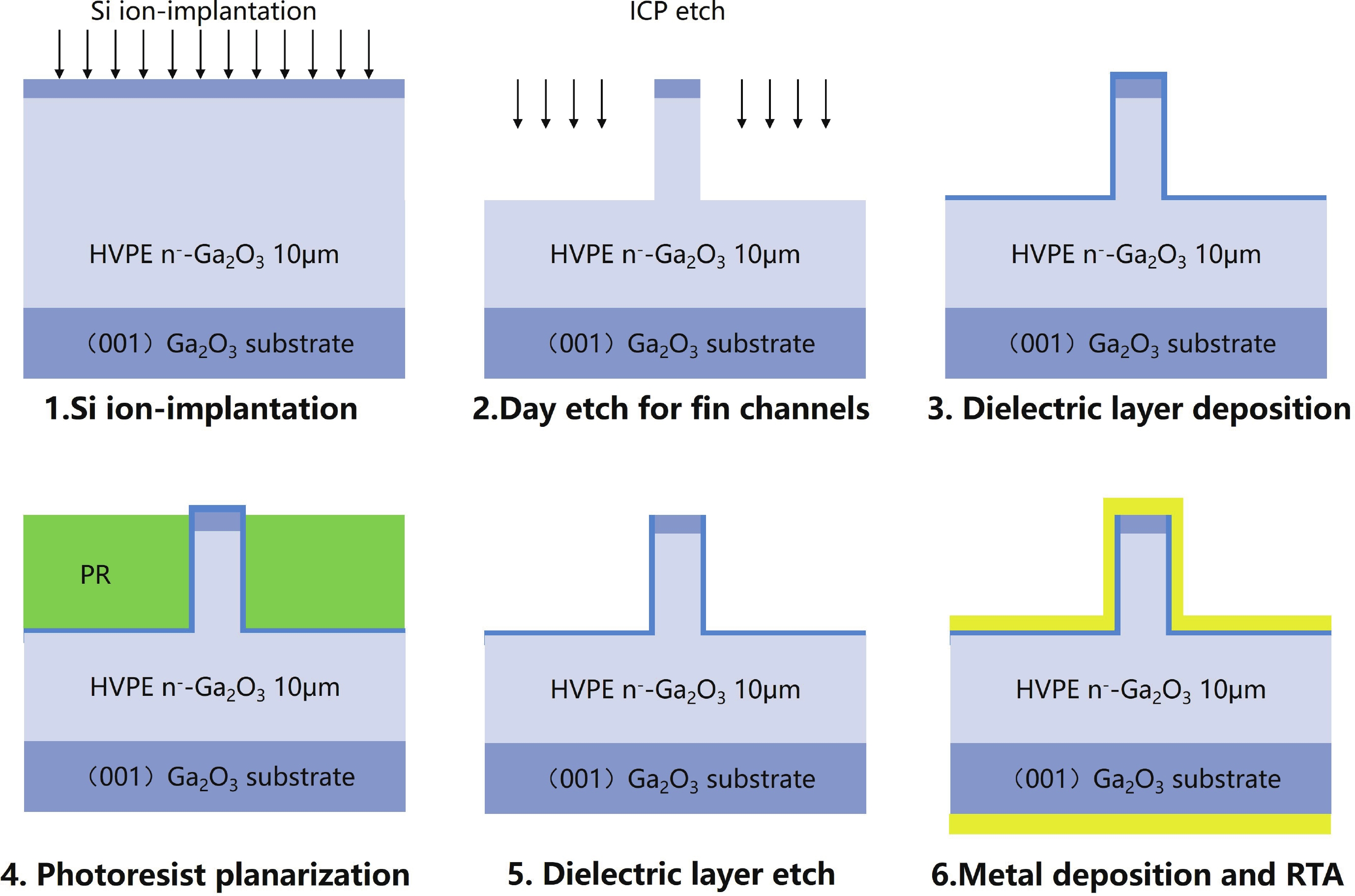
This study presents a β-Ga2O3 diode featuring a Fin-channel structure and an anode ohmic contact. The device turn-off is facilitated by the depletion effect induced by the work function difference between the sidewall metal and β-Ga2O3. As the forward bias increases, electron accumulation occurs on the Fin-channel sidewalls, reducing the on-resistance and improving the forward characteristics. Moreover, the device exhibits the reduced surface field (RESURF) effect, similar to trench schottky barrier diodes (SBDs), which shifts the electric field at the fin corners and enhances the breakdown voltage. For a device with a 100 nm fin width (Wfin), we achieved a breakdown voltage (BV) of 1137 V, a specific on-resistance (Ron,sp) of 1.8 mΩ·cm2, and a power figure of merit (PFOM) of 0.72 GW/cm2. This work expands the fabrication approach for β-Ga2O3-based devices, advancing their potential for high-performance applications.
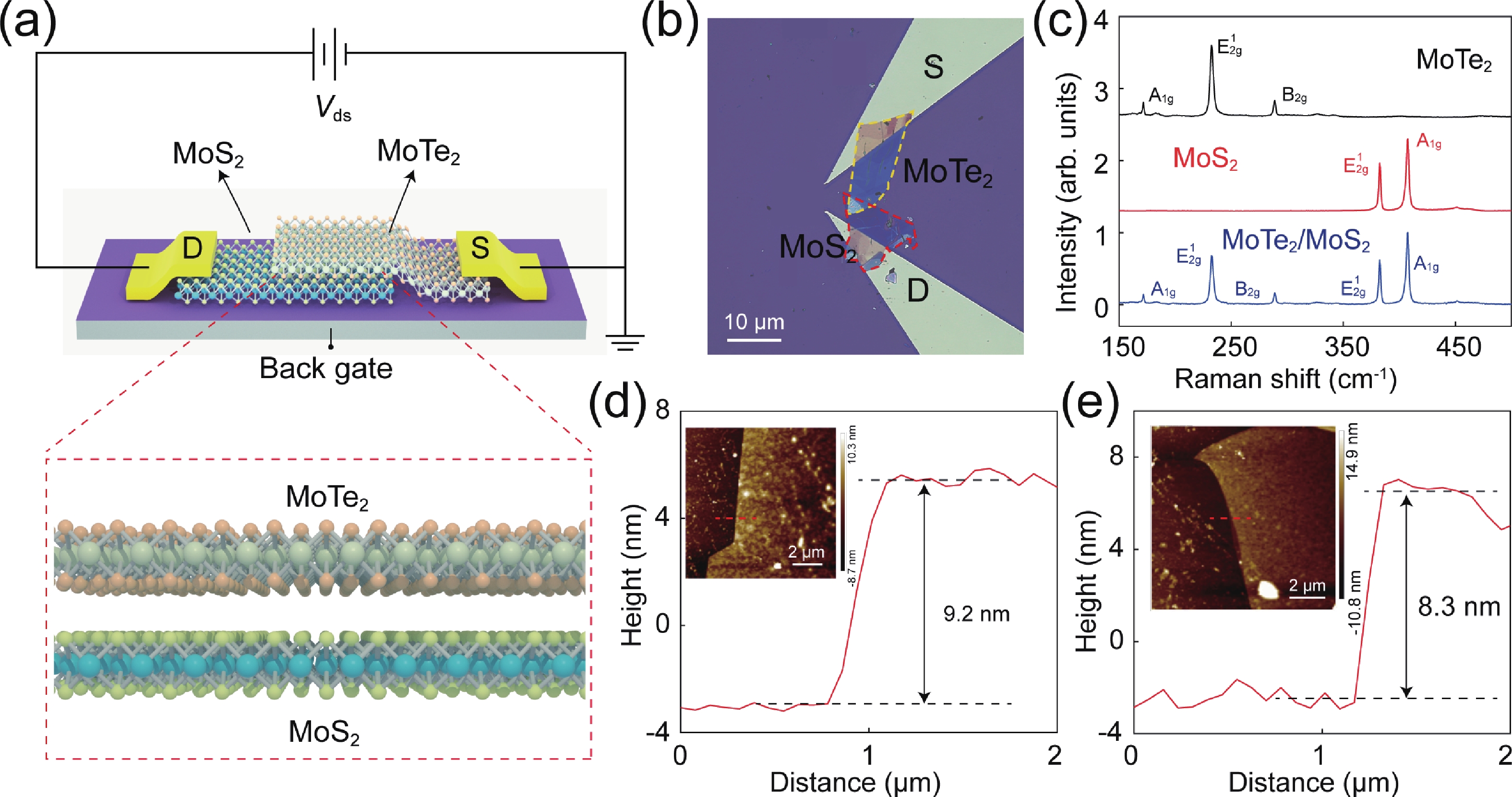
The von Neumann bottleneck in conventional computing architectures presents a significant challenge for data-intensive artificial intelligence applications. A promising approach involves designing specialized hardware with on-chip parameter tunability, which directly accelerates machine learning functions. This work demonstrates a continuously tunable mixed-kernel function physically realized within a van der Waals heterostructure. We designed and fabricated a MoTe2/MoS2 type-Ⅱ vertical heterojunction phototransistor, which exhibits a non-monotonic, Gaussian-like optoelectronic response owing to its unique interlayer charge transfer mechanism. This intrinsic physical behavior directly maps to a mixed-kernel function combining Gaussian and Sigmoid characteristics. Furthermore, the hardware kernel can be continuously modulated by in-situ tuning of external optical stimuli. The mixed-kernel exhibited exceptional performance, achieving precision, accuracy, and area under the curve (AUC) values of 95.8%, 96%, and 0.9986, respectively, significantly outperforming conventional kernels. By successfully embedding a complex, adaptable mathematical function into the intrinsic physical properties of a single device, this work pioneers a novel pathway toward next-generation, energy-efficient intelligent systems with hardware-level adaptability.


