


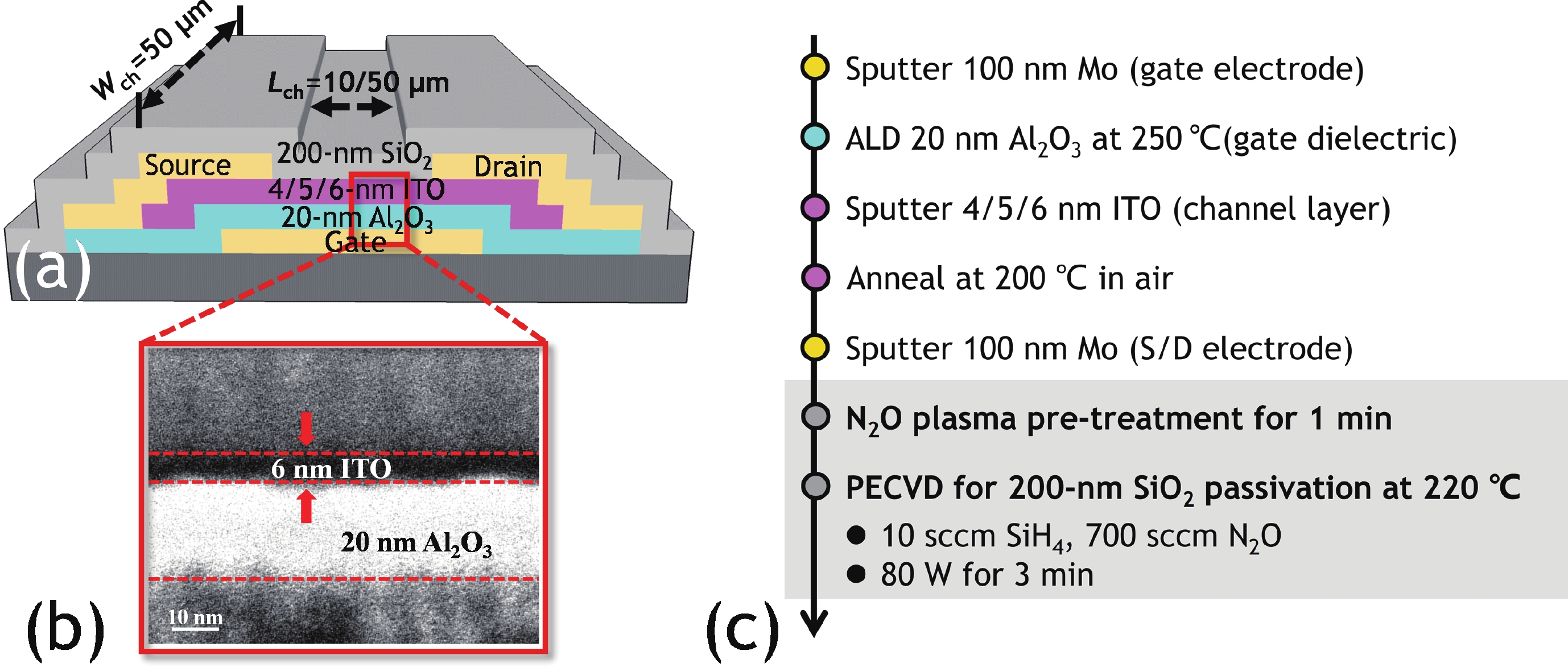
Fig. 1.
(Color online) (a) Schematic diagram of the passivated ITO TFTs with bottom-gate staggered structure. (b) TEM image of ITO TFT with tch of 6 nm. (c) Fabrication process flow of the ITO TFTs with PECVD SiO2 passivation layer.
ARTICLES
Tingrui Huang1, Jie Cao1, Zuoxu Yu1, Yuzhen Zhang1, Wenting Xu1, Xifeng Li2, Cong Peng2, Weifeng Sun1, Guangan Yang3, and Wangran Wu1,
Corresponding author: Guangan Yang, yga@njupt.edu.cn; Wangran Wu, wrwu@seu.edu.cn
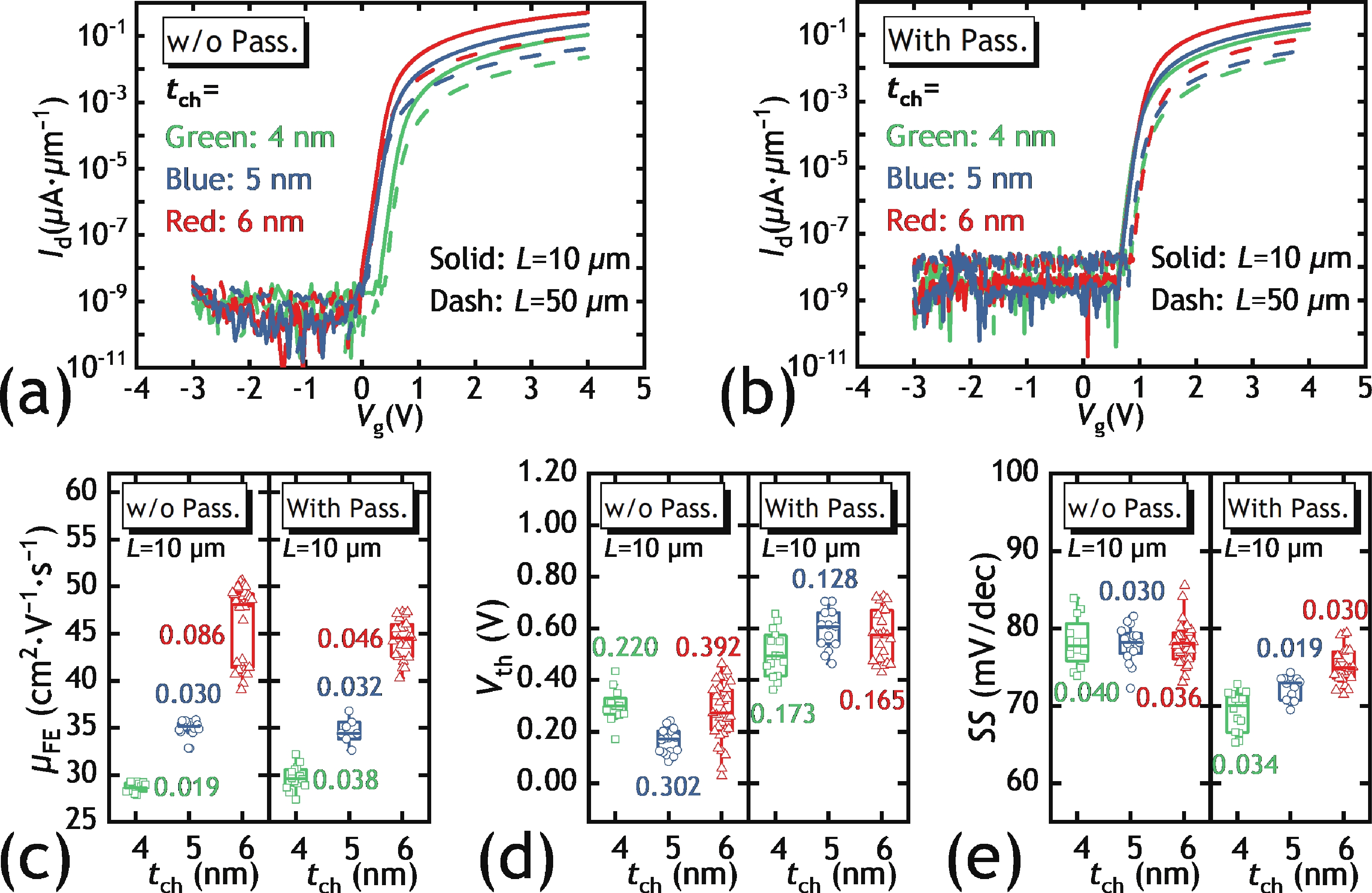
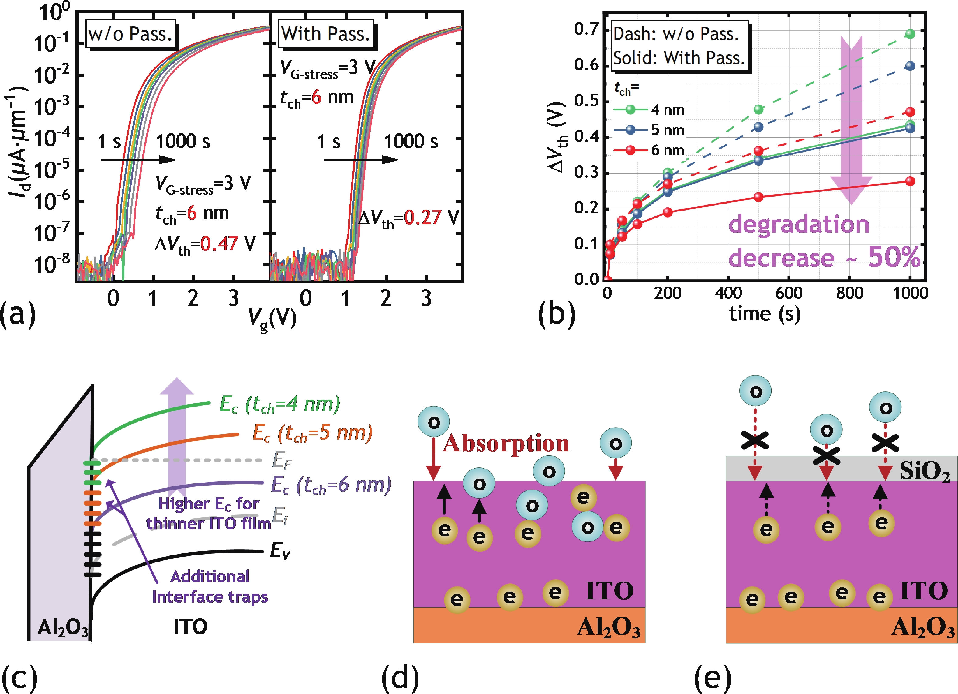
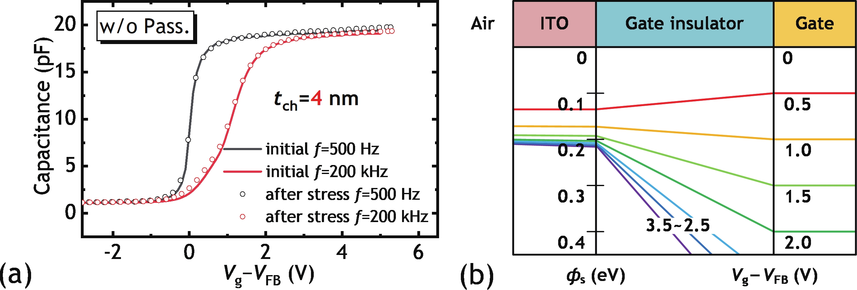
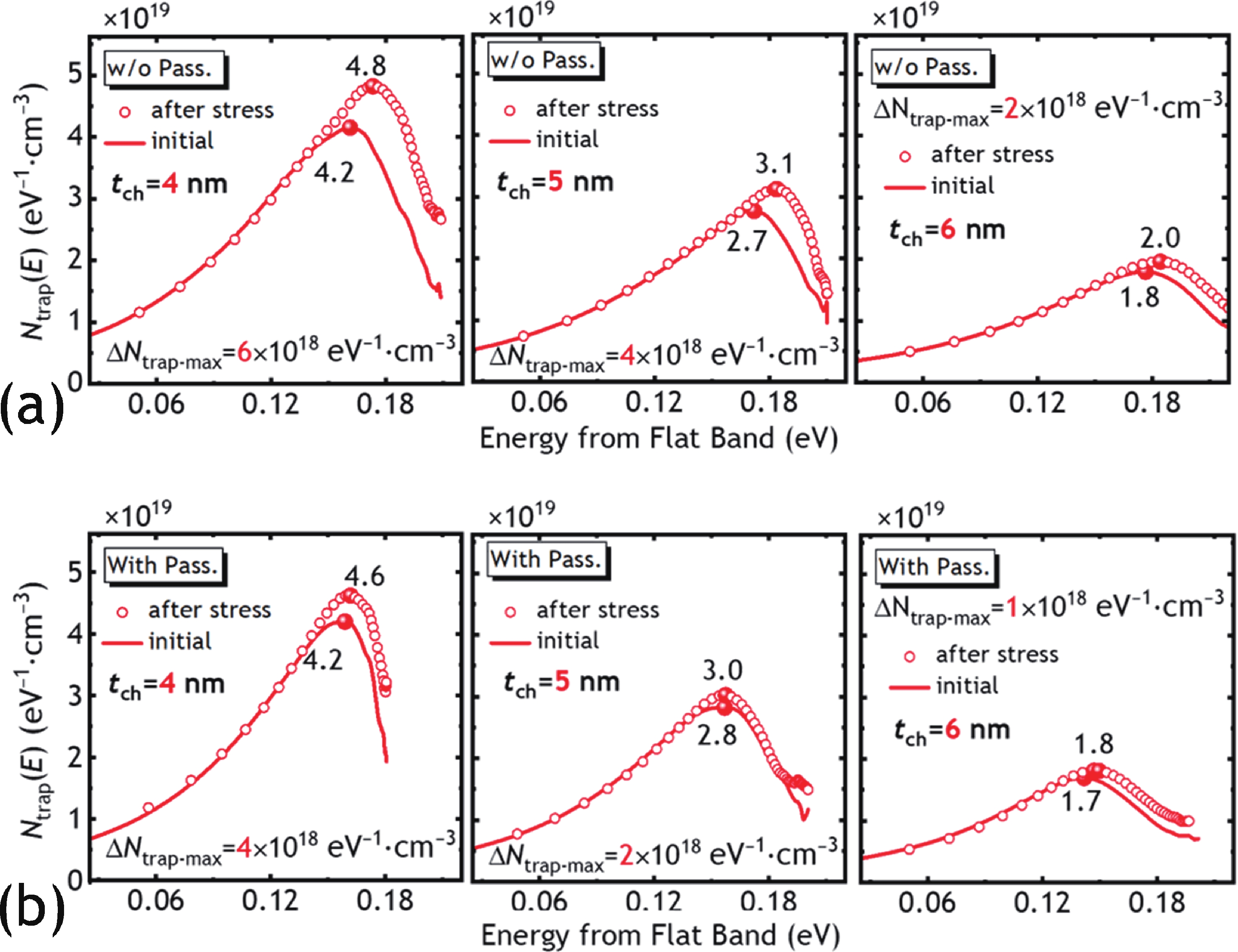
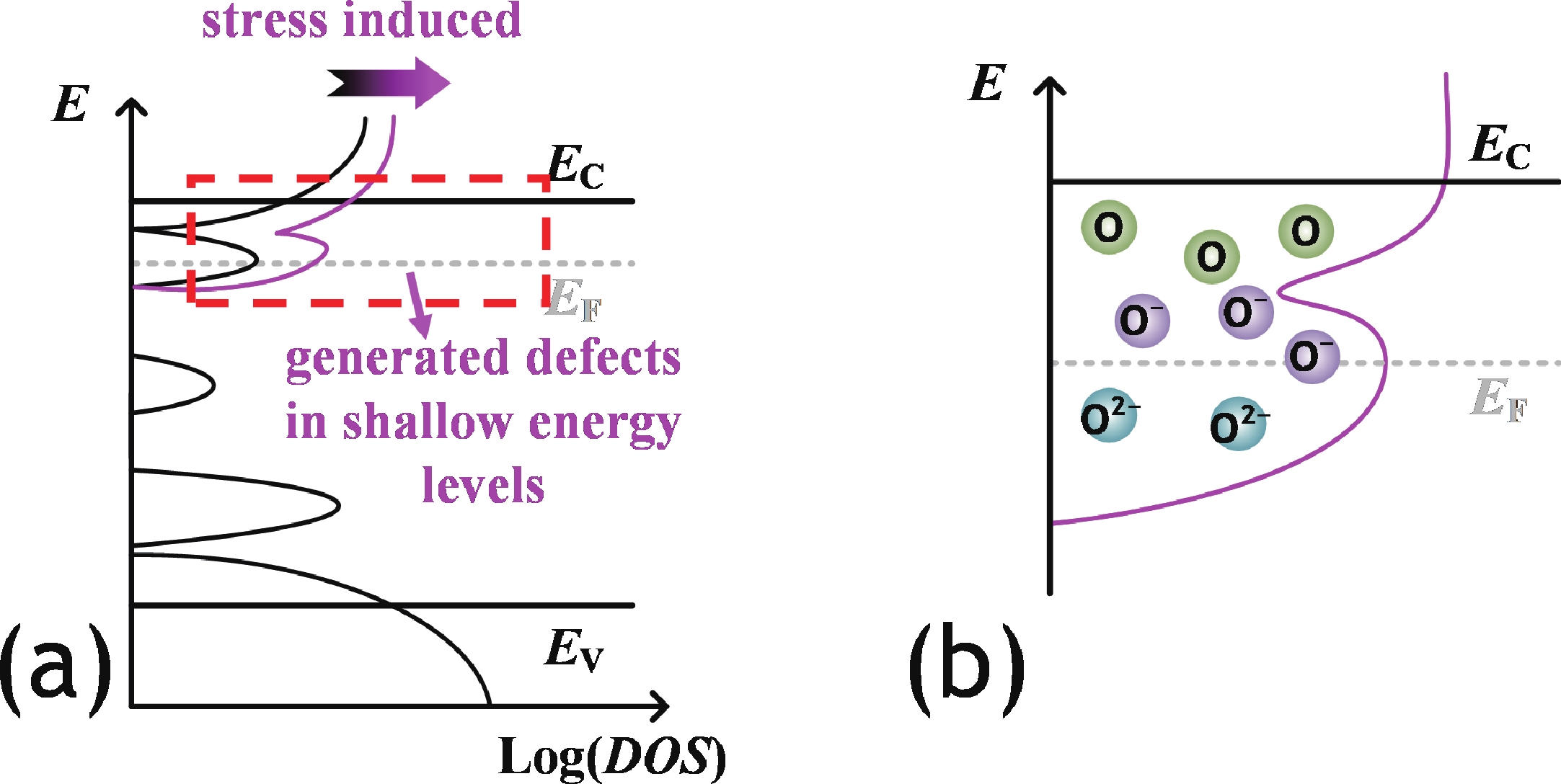
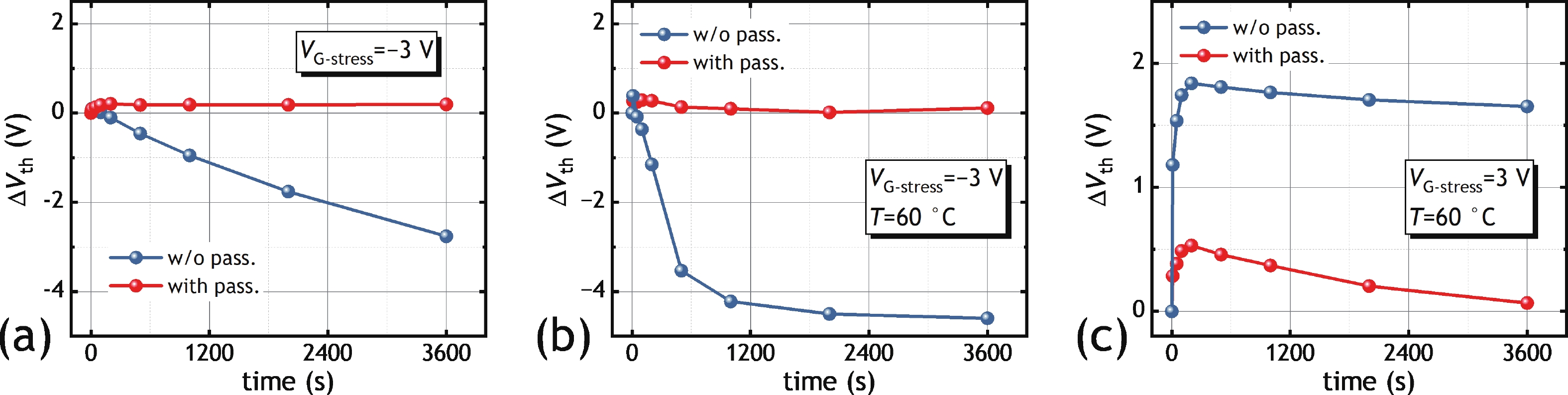
Abstract: In this work, we demonstrated the InSnO (ITO) TFTs passivated with SiO2 via the PECVD process compatible with large-area production for the first time. The passivated ITO TFTs with various channel thicknesses (tch = 4, 5, 6 nm) exhibit excellent electrical performance and superior uniformity. The reliability properties of ITO TFTs were evaluated in detail under positive bias stress (PBS) conditions before and after passivation. Compared to the devices without passivation, the passivated devices have only 50% threshold voltage degradation (ΔVth) and 50% newly generated traps due to excellent isolation of the ambient atmosphere. The negligible performance degradation of ITO TFTs with passivation during negative bias stress (NBS) and negative bias temperature stress (NBTS) verifies the outstanding immunity to the water vapor of the SiO2 passivation layer. Overall, the ITO TFT with the tch of 6 nm and with SiO2 passivation exhibits the best performance in terms of electrical properties, uniformity, and reliability, which is promising in large-area production.
Keywords: thin film transistor, reliability, InSnO, SiO2
| [1] |
Nomura K, Takagi A, Kamiya T, et al. Amorphous oxide semiconductors for high-performance flexible thin-film transistors. Jjap, 2006, 45(5S): 4303 doi: 10.1143/JJAP.45.4303
|
| [2] |
Duan X L, Huang K L, Feng J X, et al. Novel vertical channel-all-around (CAA) In-Ga-Zn-O FET for 2T0C-DRAM with high density beyond 4F2 by monolithic stacking. IEEE Trans Electron Devices, 2022, 69(4): 2196 doi: 10.1109/TED.2022.3154693
|
| [3] |
Samanta S, Chand U, Xu S Q, et al. Low subthreshold swing and high mobility amorphous indium–gallium–zinc-oxide thin-film transistor with thin HfO2 gate dielectric and excellent uniformity. IEEE Electron Device Lett, 2020, 41(6): 856 doi: 10.1109/LED.2020.2985787
|
| [4] |
Si M W, Hu Y Q, Lin Z H, et al. Why In2O3 can make 0.7 nm atomic layer thin transistors. Nano Lett, 2021, 21(1): 500 doi: 10.1021/acs.nanolett.0c03967
|
| [5] |
Si M W, Lin Z H, Charnas A, et al. Scaled atomic-layer-deposited indium oxide nanometer transistors with maximum drain current exceeding 2 A/mm at drain voltage of 0.7 V. IEEE Electron Device Lett, 2021, 42(2): 184 doi: 10.1109/LED.2020.3043430
|
| [6] |
Si M W, Lin Z H, Chen Z Z, et al. Scaled indium oxide transistors fabricated using atomic layer deposition. Nat Electron, 2022, 5: 164 doi: 10.1038/s41928-022-00718-w
|
| [7] |
Wahid S, Daus A, Kumar A, et al. First demonstration of dual-gated indium tin oxide transistors with record drive current ~ 2.3 mA/μm at L ≈ 60 nm and VDS = 1 V. 2022 International Electron Devices Meeting (IEDM), 2022: 12.5.1 doi: 10.1109/IEDM45625.2022.10019544
|
| [8] |
Oota M, Ando Y, Tsuda K, et al. 3D-stacked CAAC-In-Ga-Zn oxide FETs with gate length of 72 nm. 2019 IEEE International Electron Devices Meeting (IEDM), 2019: 3.2.1 doi: 10.1109/IEDM19573.2019.8993506
|
| [9] |
Chakraborty W, Grisafe B, Ye H C, et al. BEOL compatible dual-gate ultra thin-body W-doped indium-oxide transistor with Ion = 370 μA/μm, SS = 73 mV/dec and Ion/Ioff ratio > 4×10⁹. 2020 IEEE Symposium on VLSI Technology, 2020: 2 doi: 10.1109/VLSITechnology18217.2020.9265064
|
| [10] |
Li S M, Tian M C, Gao Q G, et al. Nanometre-thin indium tin oxide for advanced high-performance electronics. Nat Mater, 2019, 18(10): 1091 doi: 10.1038/s41563-019-0455-8
|
| [11] |
Liu G, Kong Q W, Wang X L, et al. Unveiling the influence of channel thickness on PBTI and LFN in sub-10 nm-thick IGZO FETs: A holistic perspective for advancing oxide semiconductor devices. 2023 International Electron Devices Meeting (IEDM), 2023: 1 doi: 10.1109/IEDM45741.2023.10413735
|
| [12] |
Li S M, Tian M C, Gu C R, et al. BEOL compatible 15-nm channel length ultrathin indium-tin-oxide transistors with Ion = 970 μA/μm and on/off ratio near 1011 at Vds = 0.5 V. 2019 IEEE International Electron Devices Meeting (IEDM), 2019: 3.5.1 doi: 10.1109/IEDM19573.2019.8993488
|
| [13] |
Li S M, Gu C R, Li X F, et al. 10-nm channel length indium-tin-oxide transistors with Ion = 1860 μA/μm, Gm = 1050 μS/μm at Vds = 1 V with BEOL compatibility. 2020 IEEE International Electron Devices Meeting (IEDM), 2020: 40.5.1 doi: 10.1109/IEDM13553.2020.9371966
|
| [14] |
Si M W, Andler J, Lyu X, et al. Indium–tin-oxide transistors with one nanometer thick channel and ferroelectric gating. ACS Nano, 2020, 14(9): 11542 doi: 10.1021/acsnano.0c03978
|
| [15] |
Le Y, Shao Y, Xiao X, et al. Indium–tin–oxide thin-film transistors with in situ anodized Ta2O5 passivation layer. IEEE Electron Device Lett, 2016, 37(5): 603 doi: 10.1109/LED.2016.2548785
|
| [16] |
Gao Q G, Cao T F, Li J B, et al. Enhancing electrical performance and stability of nanometer-thin ITO transistors via thermally oxidized alumina passivation layer. AIP Adv, 2023, 13(7): 075111 doi: 10.1063/5.0148763
|
| [17] |
Gao Q G, Li J B, Cao T F, et al. Effect of vacuum annealing on indium tin oxide transistor with nanometer-thin channel. Vacuum, 2024, 222: 113016 doi: 10.1016/j.vacuum.2024.113016
|
| [18] |
Park H W, Park K, Kwon J Y, et al. Effect of active layer thickness on device performance of tungsten-doped InZnO thin-film transistor. IEEE Trans Electron Devices, 2017, 64(1): 159 doi: 10.1109/TED.2016.2630043
|
| [19] |
Zhang X N, Xu L, Liang R Y, et al. Improved environmental stability of InSnO thin-film transistor by interface engineering. IEEE Trans Electron Devices, 2024, 71(5): 3015 doi: 10.1109/TED.2024.3381098
|
| [20] |
Crinon E, Evans J T. The effect of surface roughness, oxide film thickness and interfacial sliding on the electrical contact resistance of aluminium. Mater Sci Eng A, 1998, 242(1/2): 121 doi: 10.1016/S0921-5093(97)00508-X
|
| [21] |
Rabbi M H, Billah M M, Siddik A B, et al. Extremely stable dual gate coplanar amorphous InGaZnO thin film transistor with split active layer by N2O annealing. IEEE Electron Device Lett, 2020, 41(12): 1782 doi: 10.1109/LED.2020.3034119
|
| [22] |
Huang X D, Song J Q, Lai P T. Improved stability of α-InGaZnO thin-film transistor under positive gate bias stress by using fluorine plasma treatment. IEEE Electron Device Lett, 2017, 38(5): 576 doi: 10.1109/LED.2017.2678468
|
| [23] |
Um J G, Jang J. Heavily doped n-type a-IGZO by F plasma treatment and its thermal stability up to 600 °C. Appl Phys Lett, 2018, 112(16): 162104 doi: 10.1063/1.5007191
|
| [24] |
Jeong J K, Won Yang H, Jeong J H, et al. Origin of threshold voltage instability in indium-gallium-zinc oxide thin film transistors. Appl Phys Lett, 2008, 93(12): 123508 doi: 10.1063/1.2990657
|
| [25] |
Park J S, Jeong J K, Chung H J, et al. Electronic transport properties of amorphous indium-gallium-zinc oxide semiconductor upon exposure to water. Appl Phys Lett, 2008, 92(7): 072104 doi: 10.1063/1.2838380
|
| [26] |
Winter R, Ahn J, McIntyre P C, et al. New method for determining flat-band voltage in high mobility semiconductors. J Vac Sci Technol B, 2013, 31(3): 030604 doi: 10.1116/1.4802478
|
| [27] |
Kimura M, Nakanishi T, Nomura K, et al. Trap densities in amorphous-InGaZnO4 thin-film transistors. Appl Phys Lett, 2008, 92(13): 133512 doi: 10.1063/1.2904704
|
| [28] |
Lee S, Park S, Kim S, et al. Extraction of subgap density of states in amorphous InGaZnO thin-film transistors by using multifrequency capacitance–voltage characteristics. IEEE Electron Device Lett, 2010, 31(3): 231 doi: 10.1109/LED.2009.2039634
|
| [29] |
Zhang J, Lin Z H, Zhang Z C, et al. Back-end-of-line-compatible scaled InGaZnO transistors by atomic layer deposition. IEEE Trans Electron Devices, 2023, 70(12): 6651 doi: 10.1109/TED.2023.3312357
|


Article views: 939 Times PDF downloads: 189 Times Cited by: 0 Times
Received: 22 May 2025 Revised: 12 August 2025 Online: Accepted Manuscript: 03 September 2025Uncorrected proof: 10 September 2025Published: 15 February 2026
| Citation: |
Tingrui Huang, Jie Cao, Zuoxu Yu, Yuzhen Zhang, Wenting Xu, Xifeng Li, Cong Peng, Weifeng Sun, Guangan Yang, Wangran Wu. Demonstration of InSnO thin-film transistors with superior uniformity and reliability utilizing SiO2 passivation[J]. Journal of Semiconductors, 2026, 47(2): 022101. doi: 10.1088/1674-4926/25050023
****
T R Huang, J Cao, Z X Yu, Y Z Zhang, W T Xu, X F Li, C Peng, W F Sun, G G Yang, and W R Wu, Demonstration of InSnO thin-film transistors with superior uniformity and reliability utilizing SiO2 passivation[J]. J. Semicond., 2026, 47(2): 022101 doi: 10.1088/1674-4926/25050023

|
 Tingrui Huang obtained his bachelor degree from Southeast University in 2021. He is currently pursuing the Ph.D. degree with the School of Integrated Circuits, Southeast University. His research interests cover thin-film transistors
 Guangan Yang obtained his Ph.D. degree from Southeast University in 2023. His research interests cover thin-film transistors, flexible power devices, and flexible power management circuits
 Wangran Wu obtained his bachelor degree in 2011 and Ph.D. degree in 2016 from Nanjing University. In 2016, he joined the School of Electronic Science and Engineering, Southeast University. Now he is an associate professor and doctoral supervisor at the School of Integrated Circuit. His research interests cover the design and fabrication of flexible electronic devices, circuits and systems
| [1] |
Nomura K, Takagi A, Kamiya T, et al. Amorphous oxide semiconductors for high-performance flexible thin-film transistors. Jjap, 2006, 45(5S): 4303 doi: 10.1143/JJAP.45.4303
|
| [2] |
Duan X L, Huang K L, Feng J X, et al. Novel vertical channel-all-around (CAA) In-Ga-Zn-O FET for 2T0C-DRAM with high density beyond 4F2 by monolithic stacking. IEEE Trans Electron Devices, 2022, 69(4): 2196 doi: 10.1109/TED.2022.3154693
|
| [3] |
Samanta S, Chand U, Xu S Q, et al. Low subthreshold swing and high mobility amorphous indium–gallium–zinc-oxide thin-film transistor with thin HfO2 gate dielectric and excellent uniformity. IEEE Electron Device Lett, 2020, 41(6): 856 doi: 10.1109/LED.2020.2985787
|
| [4] |
Si M W, Hu Y Q, Lin Z H, et al. Why In2O3 can make 0.7 nm atomic layer thin transistors. Nano Lett, 2021, 21(1): 500 doi: 10.1021/acs.nanolett.0c03967
|
| [5] |
Si M W, Lin Z H, Charnas A, et al. Scaled atomic-layer-deposited indium oxide nanometer transistors with maximum drain current exceeding 2 A/mm at drain voltage of 0.7 V. IEEE Electron Device Lett, 2021, 42(2): 184 doi: 10.1109/LED.2020.3043430
|
| [6] |
Si M W, Lin Z H, Chen Z Z, et al. Scaled indium oxide transistors fabricated using atomic layer deposition. Nat Electron, 2022, 5: 164 doi: 10.1038/s41928-022-00718-w
|
| [7] |
Wahid S, Daus A, Kumar A, et al. First demonstration of dual-gated indium tin oxide transistors with record drive current ~ 2.3 mA/μm at L ≈ 60 nm and VDS = 1 V. 2022 International Electron Devices Meeting (IEDM), 2022: 12.5.1 doi: 10.1109/IEDM45625.2022.10019544
|
| [8] |
Oota M, Ando Y, Tsuda K, et al. 3D-stacked CAAC-In-Ga-Zn oxide FETs with gate length of 72 nm. 2019 IEEE International Electron Devices Meeting (IEDM), 2019: 3.2.1 doi: 10.1109/IEDM19573.2019.8993506
|
| [9] |
Chakraborty W, Grisafe B, Ye H C, et al. BEOL compatible dual-gate ultra thin-body W-doped indium-oxide transistor with Ion = 370 μA/μm, SS = 73 mV/dec and Ion/Ioff ratio > 4×10⁹. 2020 IEEE Symposium on VLSI Technology, 2020: 2 doi: 10.1109/VLSITechnology18217.2020.9265064
|
| [10] |
Li S M, Tian M C, Gao Q G, et al. Nanometre-thin indium tin oxide for advanced high-performance electronics. Nat Mater, 2019, 18(10): 1091 doi: 10.1038/s41563-019-0455-8
|
| [11] |
Liu G, Kong Q W, Wang X L, et al. Unveiling the influence of channel thickness on PBTI and LFN in sub-10 nm-thick IGZO FETs: A holistic perspective for advancing oxide semiconductor devices. 2023 International Electron Devices Meeting (IEDM), 2023: 1 doi: 10.1109/IEDM45741.2023.10413735
|
| [12] |
Li S M, Tian M C, Gu C R, et al. BEOL compatible 15-nm channel length ultrathin indium-tin-oxide transistors with Ion = 970 μA/μm and on/off ratio near 1011 at Vds = 0.5 V. 2019 IEEE International Electron Devices Meeting (IEDM), 2019: 3.5.1 doi: 10.1109/IEDM19573.2019.8993488
|
| [13] |
Li S M, Gu C R, Li X F, et al. 10-nm channel length indium-tin-oxide transistors with Ion = 1860 μA/μm, Gm = 1050 μS/μm at Vds = 1 V with BEOL compatibility. 2020 IEEE International Electron Devices Meeting (IEDM), 2020: 40.5.1 doi: 10.1109/IEDM13553.2020.9371966
|
| [14] |
Si M W, Andler J, Lyu X, et al. Indium–tin-oxide transistors with one nanometer thick channel and ferroelectric gating. ACS Nano, 2020, 14(9): 11542 doi: 10.1021/acsnano.0c03978
|
| [15] |
Le Y, Shao Y, Xiao X, et al. Indium–tin–oxide thin-film transistors with in situ anodized Ta2O5 passivation layer. IEEE Electron Device Lett, 2016, 37(5): 603 doi: 10.1109/LED.2016.2548785
|
| [16] |
Gao Q G, Cao T F, Li J B, et al. Enhancing electrical performance and stability of nanometer-thin ITO transistors via thermally oxidized alumina passivation layer. AIP Adv, 2023, 13(7): 075111 doi: 10.1063/5.0148763
|
| [17] |
Gao Q G, Li J B, Cao T F, et al. Effect of vacuum annealing on indium tin oxide transistor with nanometer-thin channel. Vacuum, 2024, 222: 113016 doi: 10.1016/j.vacuum.2024.113016
|
| [18] |
Park H W, Park K, Kwon J Y, et al. Effect of active layer thickness on device performance of tungsten-doped InZnO thin-film transistor. IEEE Trans Electron Devices, 2017, 64(1): 159 doi: 10.1109/TED.2016.2630043
|
| [19] |
Zhang X N, Xu L, Liang R Y, et al. Improved environmental stability of InSnO thin-film transistor by interface engineering. IEEE Trans Electron Devices, 2024, 71(5): 3015 doi: 10.1109/TED.2024.3381098
|
| [20] |
Crinon E, Evans J T. The effect of surface roughness, oxide film thickness and interfacial sliding on the electrical contact resistance of aluminium. Mater Sci Eng A, 1998, 242(1/2): 121 doi: 10.1016/S0921-5093(97)00508-X
|
| [21] |
Rabbi M H, Billah M M, Siddik A B, et al. Extremely stable dual gate coplanar amorphous InGaZnO thin film transistor with split active layer by N2O annealing. IEEE Electron Device Lett, 2020, 41(12): 1782 doi: 10.1109/LED.2020.3034119
|
| [22] |
Huang X D, Song J Q, Lai P T. Improved stability of α-InGaZnO thin-film transistor under positive gate bias stress by using fluorine plasma treatment. IEEE Electron Device Lett, 2017, 38(5): 576 doi: 10.1109/LED.2017.2678468
|
| [23] |
Um J G, Jang J. Heavily doped n-type a-IGZO by F plasma treatment and its thermal stability up to 600 °C. Appl Phys Lett, 2018, 112(16): 162104 doi: 10.1063/1.5007191
|
| [24] |
Jeong J K, Won Yang H, Jeong J H, et al. Origin of threshold voltage instability in indium-gallium-zinc oxide thin film transistors. Appl Phys Lett, 2008, 93(12): 123508 doi: 10.1063/1.2990657
|
| [25] |
Park J S, Jeong J K, Chung H J, et al. Electronic transport properties of amorphous indium-gallium-zinc oxide semiconductor upon exposure to water. Appl Phys Lett, 2008, 92(7): 072104 doi: 10.1063/1.2838380
|
| [26] |
Winter R, Ahn J, McIntyre P C, et al. New method for determining flat-band voltage in high mobility semiconductors. J Vac Sci Technol B, 2013, 31(3): 030604 doi: 10.1116/1.4802478
|
| [27] |
Kimura M, Nakanishi T, Nomura K, et al. Trap densities in amorphous-InGaZnO4 thin-film transistors. Appl Phys Lett, 2008, 92(13): 133512 doi: 10.1063/1.2904704
|
| [28] |
Lee S, Park S, Kim S, et al. Extraction of subgap density of states in amorphous InGaZnO thin-film transistors by using multifrequency capacitance–voltage characteristics. IEEE Electron Device Lett, 2010, 31(3): 231 doi: 10.1109/LED.2009.2039634
|
| [29] |
Zhang J, Lin Z H, Zhang Z C, et al. Back-end-of-line-compatible scaled InGaZnO transistors by atomic layer deposition. IEEE Trans Electron Devices, 2023, 70(12): 6651 doi: 10.1109/TED.2023.3312357
|

 WeChat ID
Journal of Semiconductors © 2017 All Rights Reserved 京ICP备05085259号-2

 DownLoad:

