


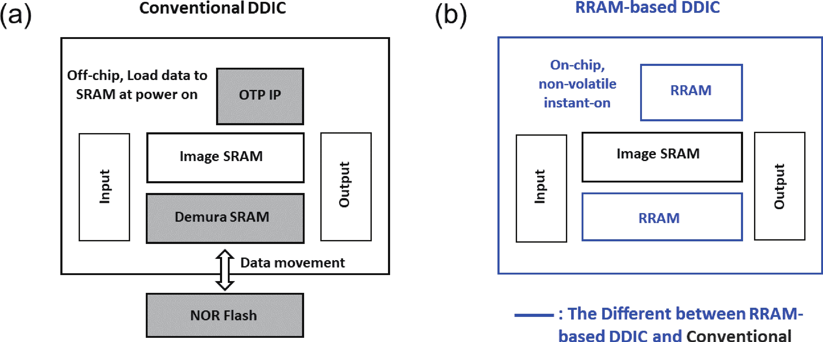
Fig. 1.
(Color online) Illustration of (a) conventional DDIC and (b) RRAM-based DDIC.
ARTICLES
Zhenchao Sui1, 2, Yanqing Wu1, Zhichao Lv3 and Xing Zhang1,
Corresponding author: Xing Zhang, zhx@pku.edu.cn
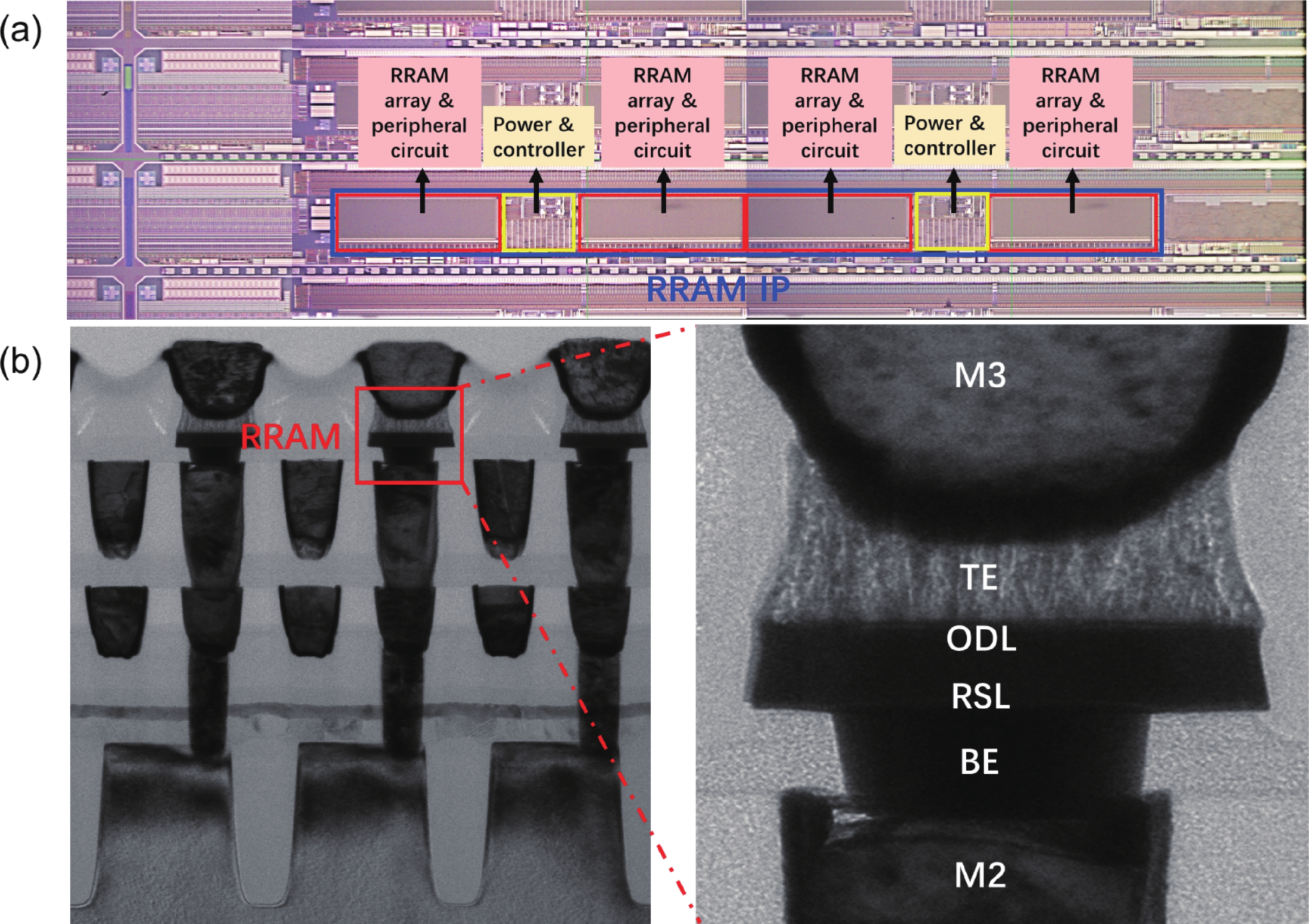
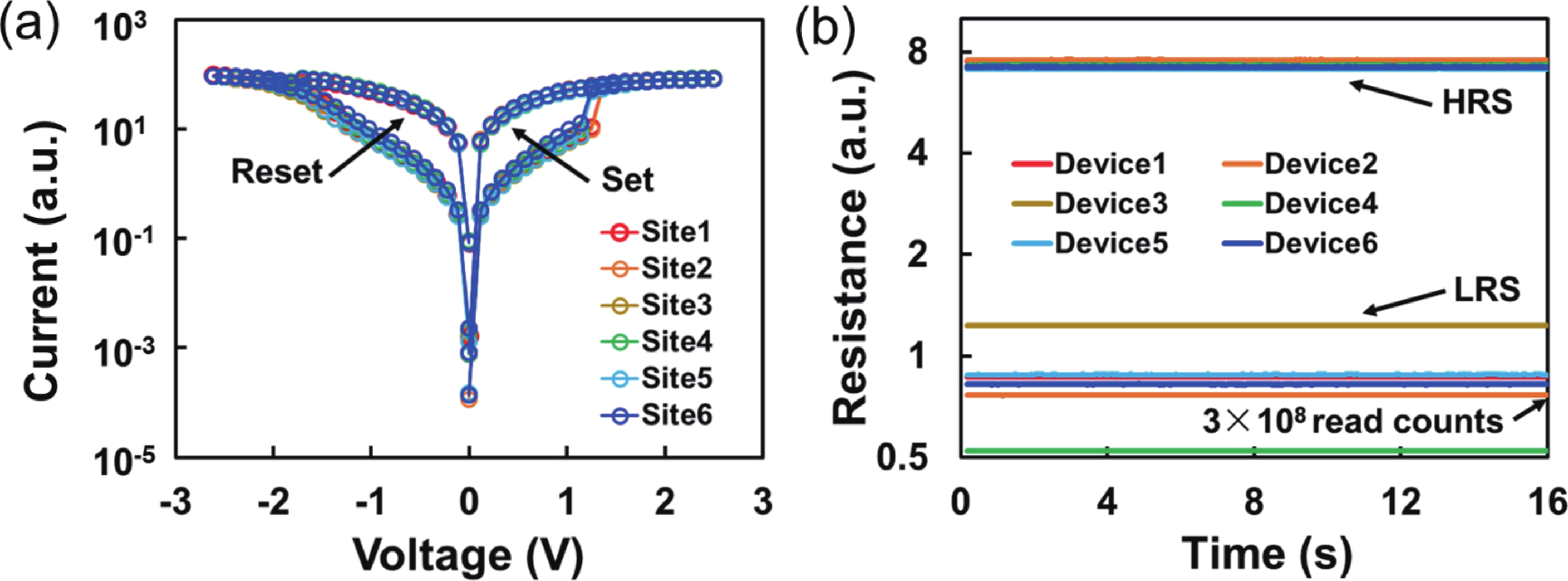
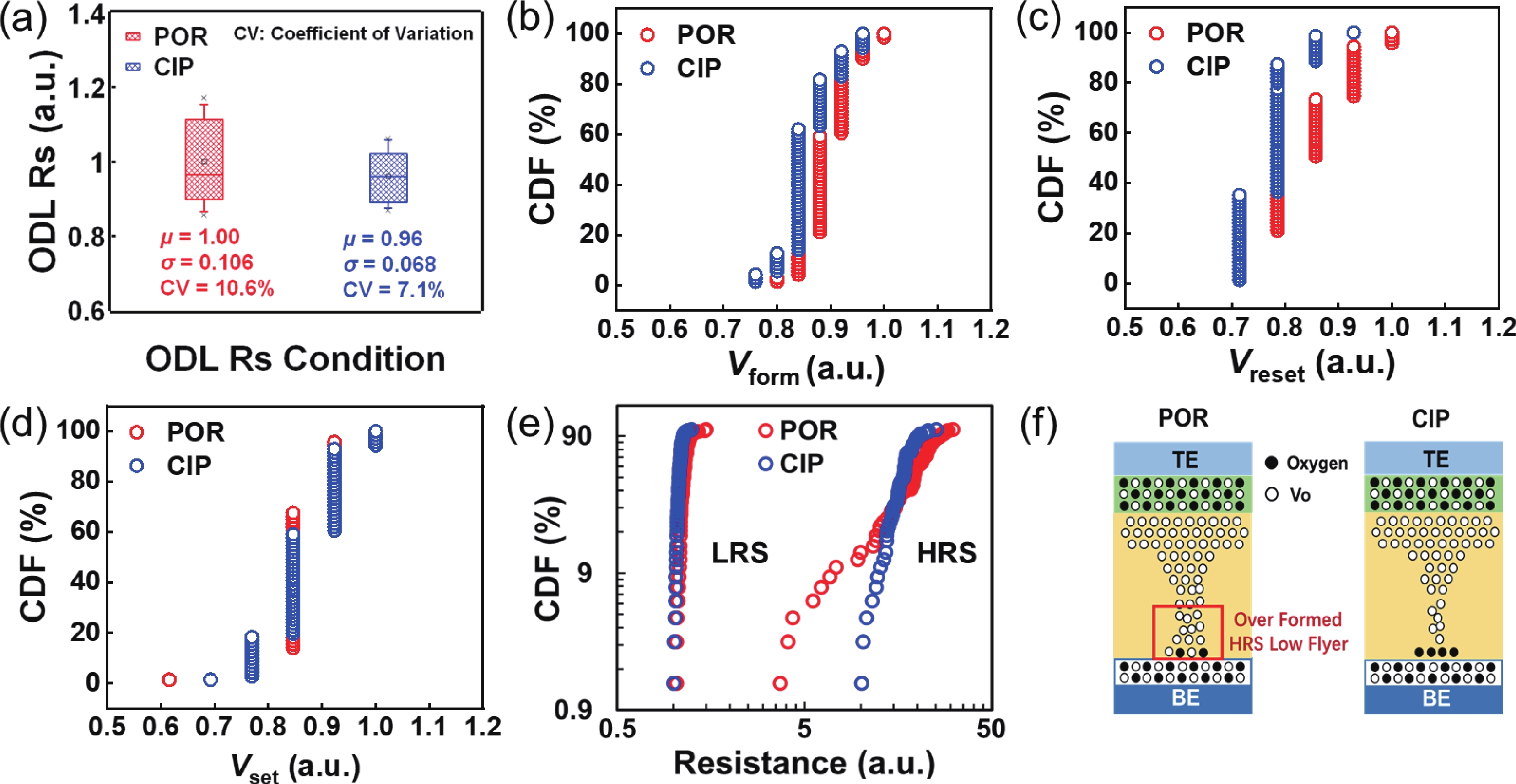
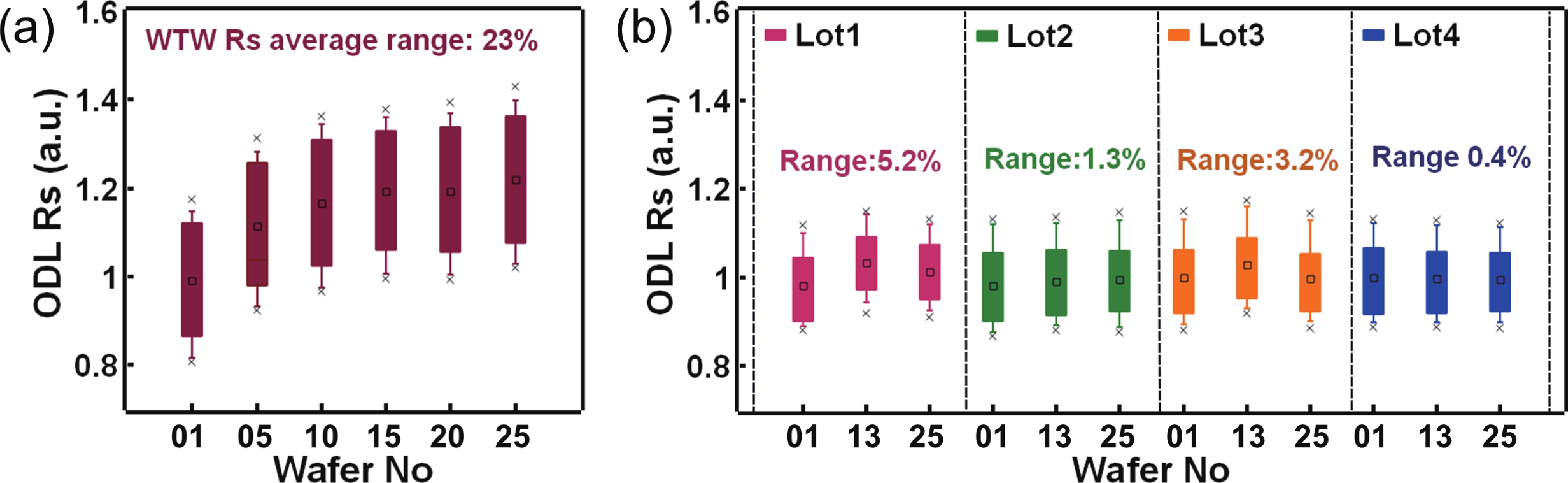
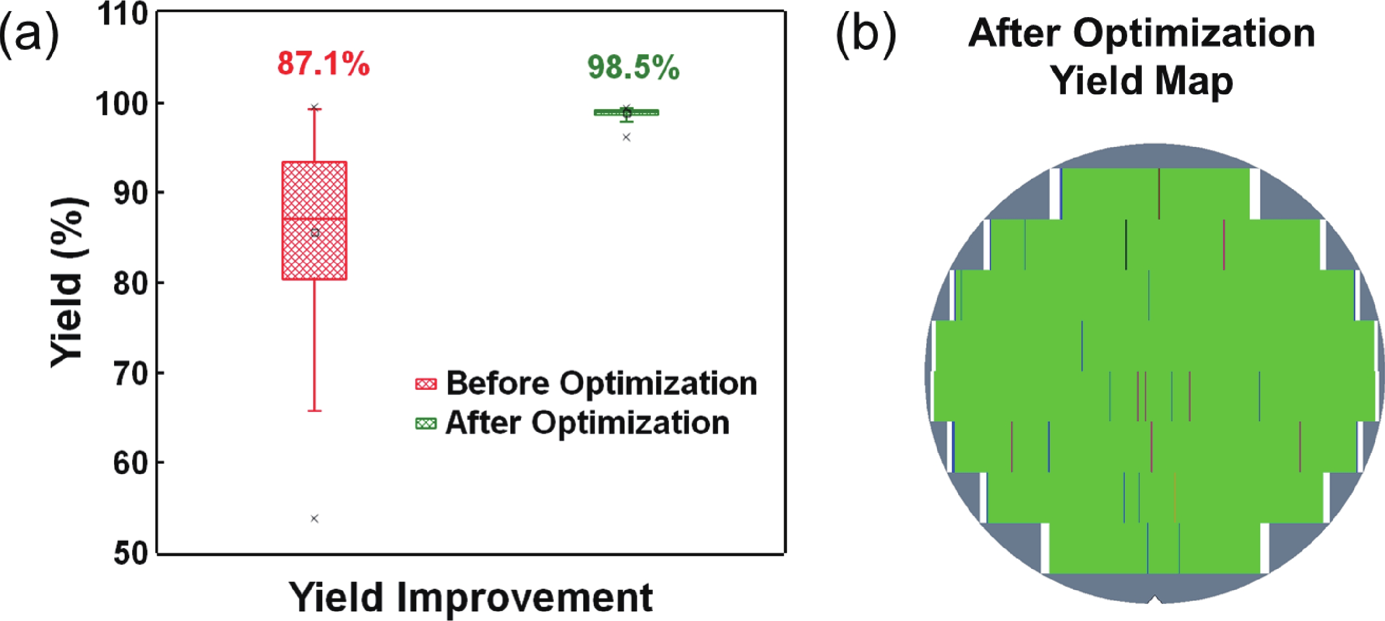
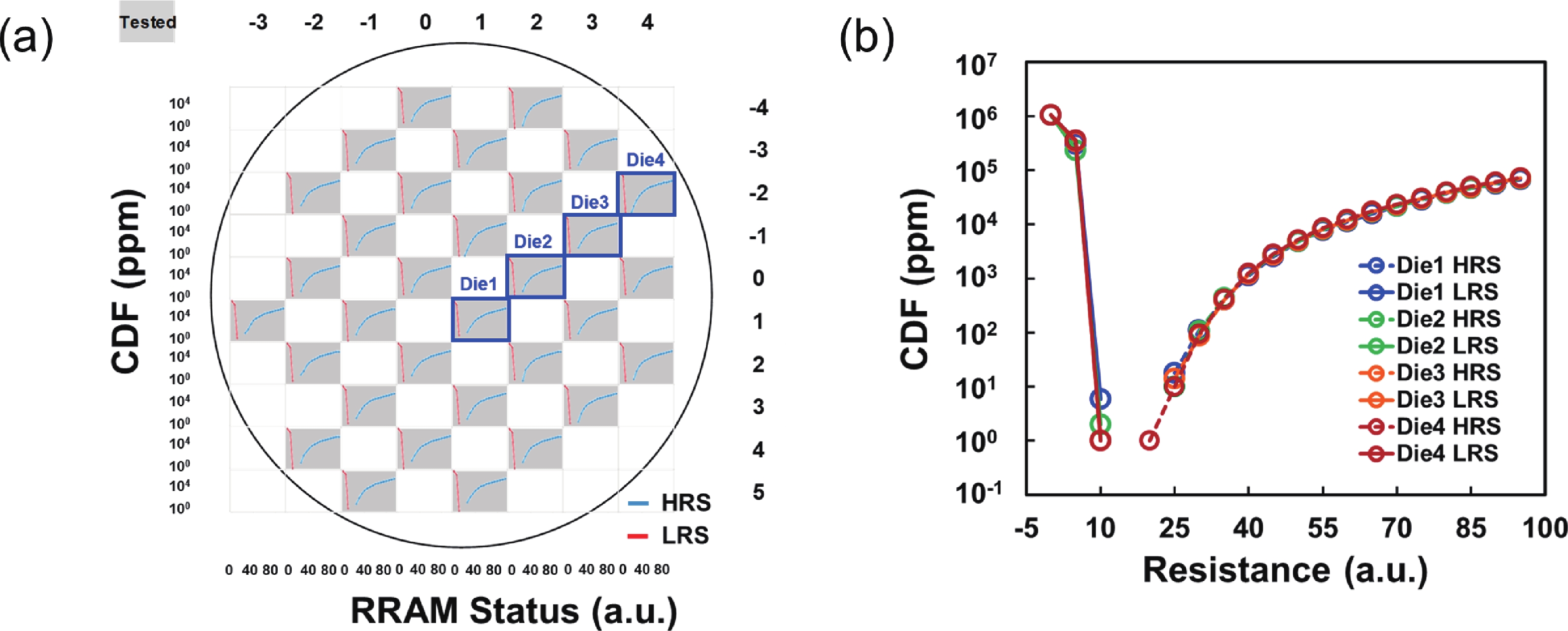
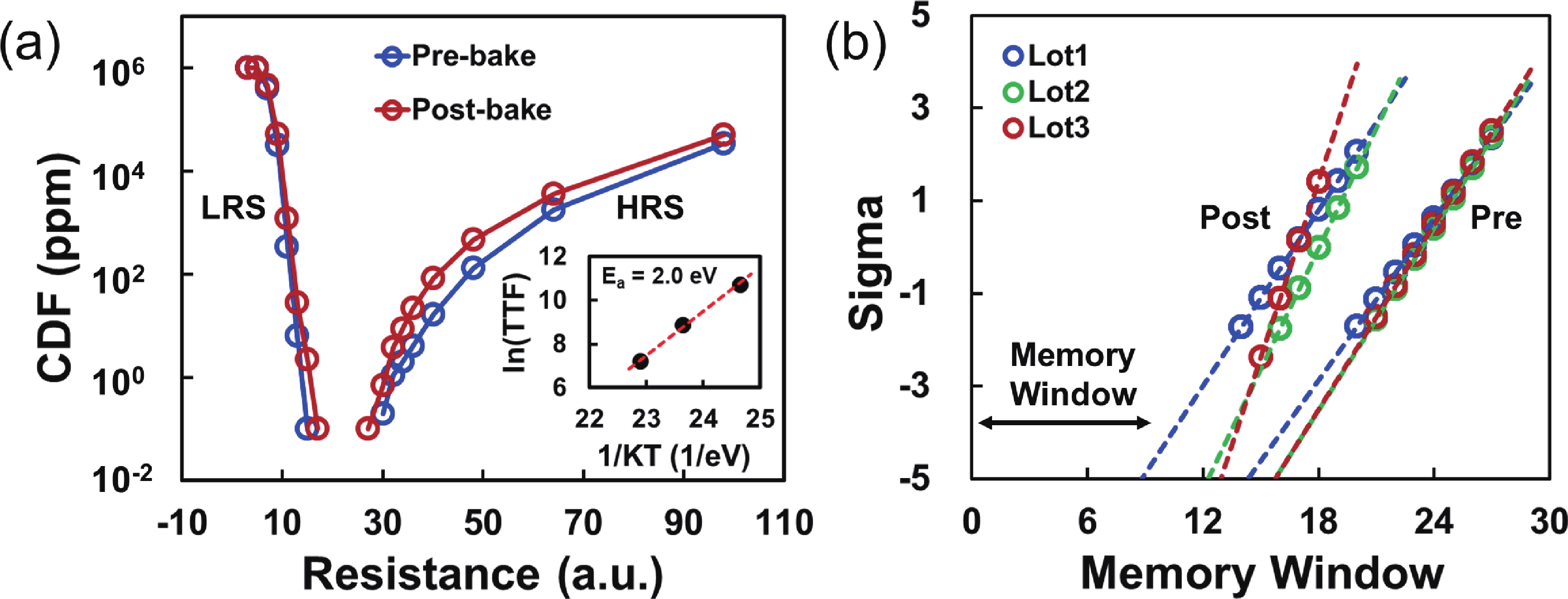
Abstract: To address the challenges of complexity, power consumption, and cost constraints in traditional display driver integrated circuits (DDICs) caused by external NOR Flash and SRAM, this work proposes an embedded resistive random-access memory (RRAM) integration solution based on a 40 nm high-voltage CMOS logic platform. Targeting the yield fluctuations and stability challenges during RRAM mass production, systematic process optimizations are implemented to achieve synergistic improvements in RRAM performance and yield. Through modifications to the film sputtering and pre-deposition treatment, the within-wafer resistance uniformity (RSU) of the oxygen-deficient layer (ODL) thin film is improved from 11% to 8%, while inter-wafer process stability variation reduces from 23% to below 6%. Consequently, the yield of 8 Mb RRAM embedded mass production products increases from 87% to 98.5%. In terms of device performance, the RRAM demonstrates a fast 4.8 ns read speed, exceptional read disturb immunity of 3 × 10⁸ cycles at 95 °C, 103 write/erase endurance cycles for the 1 Mb cells, and data retention of 12.5 years at 125 °C. Post high-temperature operating life (HTOL) testing exhibits stable high/low resistance window. This study provides process optimization strategies and a reliability assurance framework for the mass production of highly integrated, low-power embedded RRAM display driver IC.
Keywords: embedded RRAM, 40 nm CMOS, display driver IC, process uniformity optimization, yield improvement
| [1] |
Zhang P L, Shi Y S, et al. Research status and progress of high power backlight LED driving circuit. Chinese Journal of Liquid Crystals and Displays (CJLCD), 2010, 25(1): 68 (in Chinese)
|
| [2] |
Ahn Y S, Park J M, Kang J K, et al. A ±0.48°C (3σ) inaccuracy BJT-based temperature sensor with 241 μs conversion time for display driver IC in 40 nm CMOS. IEEE Access, 2023, 11: 132843 doi: 10.1109/ACCESS.2023.3335044
|
| [3] |
He Y, Ma C X, Ma X C, et al. A 3.75Mb embedded RRAM IP on 40nm high-voltage CMOS technology. 2024 IEEE International Memory Workshop (IMW), 2024: 1 doi: 10.1109/IMW59701.2024.10536978
|
| [4] |
Tsujimura T. New OLED applications. OLED display fundamentals and applications. Wiley, 2017: 235 doi: 10.1002/9781119187493.ch8
|
| [5] |
Zhang Y, Mao J X, Wang Y N, et al. An efficient optical Mura compensation system for large liquid-crystal display panels. IEEE Trans Instrum Meas, 2022, 71: 5023213 doi: 10.1109/TIM.2022.3192293
|
| [6] |
Lin C Y, Lin P F, Chung W K, et al. ResUnet-GAN with dynamic memory for mura defect detection. 2023 IEEE International Conference on Industry 4.0. Artificial Intelligence, and Communications Technology (IAICT), 2023: 350 doi: 10.1109/IAICT59002.2023.10205662
|
| [7] |
Pi S, Li C, Jiang H, et al. Memristor crossbar arrays with 6-nm half-pitch and 2-nm critical dimension. Nat Nanotechnol, 2019, 14(1): 35 doi: 10.1038/s41565-018-0302-0
|
| [8] |
Chen Y Y. ReRAM: History, Status, and Future. IEEE Trans Electron Devices, 2020, 67(4): 1420 doi: 10.1109/TED.2019.2961505
|
| [9] |
Dittmann R, Menzel S, Waser R. Nanoionic memristive phenomena in metal oxides: the valence change mechanism. Adv Phys, 2021, 70(2): 155 doi: 10.1080/00018732.2022.2084006
|
| [10] |
Shirota R. 8-3D-NAND flash memory and technology. Advances in non-volatile memory and storage technology. Amsterdam: Elsevier, 2019: 283 doi: 10.1016/B978-0-08-102584-0.00009-7
|
| [11] |
Li Y, Quader K N. NAND flash memory: challenges and opportunities. Computer, 2013, 46(8): 23 doi: 10.1109/MC.2013.190
|
| [12] |
Luo H C, Tugrul Y C, Botstancι F N, et al. Ramulator 2.0: A modern, modular, and extensible DRAM simulator. IEEE Comput Archit Lett, 2024, 23(1): 112 doi: 10.1109/LCA.2023.3333759
|
| [13] |
Kaul A, Luo Y D, Peng X C, et al. 3-D heterogeneous integration of RRAM-based compute-in-memory: Impact of integration parameters on inference accuracy. IEEE Trans Electron Devices, 2023, 70(2): 485 doi: 10.1109/TED.2022.3231570
|
| [14] |
Zhao L, Chen Z, Manea D, et al. Highly reliable 40nm embedded dual-interface-switching RRAM technology for display driver IC applications. 2022 IEEE Symposium on VLSI Technology and Circuits (VLSI Technology and Circuits), 2022: 316 doi: 10.1109/VLSITechnologyandCir46769.2022.9830289
|
| [15] |
Liu M G, Li Z, Lu W D, et al. First demonstration of monolithic three-dimensional integration of ultra-high density hybrid IGZO/Si SRAM and IGZO 2T0C DRAM achieving record-low latency (<10ns), record-low energy (<10fJ) of data transfer and ultra-long data retention (>5000s). 2024 IEEE Symposium on VLSI Technology and Circuits (VLSI Technology and Circuits), 2024: 1 doi: 10.1109/VLSITechnologyandCir46783.2024.10631551
|
| [16] |
GlobalFoundries® and microchip announce microchip's 28-nm SuperFlash® embedded flash memory solution in production. https://www.sst.com/press-releases/globalfoundries-microchip-announce-microchips-28nm-superflash/
|


Article views: 1097 Times PDF downloads: 116 Times Cited by: 0 Times
Received: 23 October 2025 Revised: 01 December 2025 Online: Accepted Manuscript: 25 December 2025Uncorrected proof: 26 December 2025Published: 15 March 2026
| Citation: |
Zhenchao Sui, Yanqing Wu, Zhichao Lv, Xing Zhang. Synergistic performance and yield improvement of embedded RRAM product through process optimization in 40 nm CMOS platform[J]. Journal of Semiconductors, 2026, 47(3): 032303. doi: 10.1088/1674-4926/25100021
****
Z C Sui, Y Q Wu, Z C Lv, and X Zhang, Synergistic performance and yield improvement of embedded RRAM product through process optimization in 40 nm CMOS platform[J]. J. Semicond., 2026, 47(3): 032303 doi: 10.1088/1674-4926/25100021

|
 Zhenchao Sui got his BS from Xi'an University of Technology in 2003 and MS from Peking University in 2008. He is now a PhD student at Peking University under the supervision of Prof. Xing Zhang. His research focus is on the performance and yield improvement of embedded-RRAM in CMOS platform
 Xing Zhang got his BS from Nanjing University in 1986, M.S. and Ph.D. degree from Shanxi Institute of Microelectronics, China, in 1989 and 1993, respectively. He joined Peking University in 1993 and is now a professor. His current research interests include the physics and novel structures of nano-scaled MOS devices, model and simulation, CMOS Integrated Circuit design and Manufacturing technology
| [1] |
Zhang P L, Shi Y S, et al. Research status and progress of high power backlight LED driving circuit. Chinese Journal of Liquid Crystals and Displays (CJLCD), 2010, 25(1): 68 (in Chinese)
|
| [2] |
Ahn Y S, Park J M, Kang J K, et al. A ±0.48°C (3σ) inaccuracy BJT-based temperature sensor with 241 μs conversion time for display driver IC in 40 nm CMOS. IEEE Access, 2023, 11: 132843 doi: 10.1109/ACCESS.2023.3335044
|
| [3] |
He Y, Ma C X, Ma X C, et al. A 3.75Mb embedded RRAM IP on 40nm high-voltage CMOS technology. 2024 IEEE International Memory Workshop (IMW), 2024: 1 doi: 10.1109/IMW59701.2024.10536978
|
| [4] |
Tsujimura T. New OLED applications. OLED display fundamentals and applications. Wiley, 2017: 235 doi: 10.1002/9781119187493.ch8
|
| [5] |
Zhang Y, Mao J X, Wang Y N, et al. An efficient optical Mura compensation system for large liquid-crystal display panels. IEEE Trans Instrum Meas, 2022, 71: 5023213 doi: 10.1109/TIM.2022.3192293
|
| [6] |
Lin C Y, Lin P F, Chung W K, et al. ResUnet-GAN with dynamic memory for mura defect detection. 2023 IEEE International Conference on Industry 4.0. Artificial Intelligence, and Communications Technology (IAICT), 2023: 350 doi: 10.1109/IAICT59002.2023.10205662
|
| [7] |
Pi S, Li C, Jiang H, et al. Memristor crossbar arrays with 6-nm half-pitch and 2-nm critical dimension. Nat Nanotechnol, 2019, 14(1): 35 doi: 10.1038/s41565-018-0302-0
|
| [8] |
Chen Y Y. ReRAM: History, Status, and Future. IEEE Trans Electron Devices, 2020, 67(4): 1420 doi: 10.1109/TED.2019.2961505
|
| [9] |
Dittmann R, Menzel S, Waser R. Nanoionic memristive phenomena in metal oxides: the valence change mechanism. Adv Phys, 2021, 70(2): 155 doi: 10.1080/00018732.2022.2084006
|
| [10] |
Shirota R. 8-3D-NAND flash memory and technology. Advances in non-volatile memory and storage technology. Amsterdam: Elsevier, 2019: 283 doi: 10.1016/B978-0-08-102584-0.00009-7
|
| [11] |
Li Y, Quader K N. NAND flash memory: challenges and opportunities. Computer, 2013, 46(8): 23 doi: 10.1109/MC.2013.190
|
| [12] |
Luo H C, Tugrul Y C, Botstancι F N, et al. Ramulator 2.0: A modern, modular, and extensible DRAM simulator. IEEE Comput Archit Lett, 2024, 23(1): 112 doi: 10.1109/LCA.2023.3333759
|
| [13] |
Kaul A, Luo Y D, Peng X C, et al. 3-D heterogeneous integration of RRAM-based compute-in-memory: Impact of integration parameters on inference accuracy. IEEE Trans Electron Devices, 2023, 70(2): 485 doi: 10.1109/TED.2022.3231570
|
| [14] |
Zhao L, Chen Z, Manea D, et al. Highly reliable 40nm embedded dual-interface-switching RRAM technology for display driver IC applications. 2022 IEEE Symposium on VLSI Technology and Circuits (VLSI Technology and Circuits), 2022: 316 doi: 10.1109/VLSITechnologyandCir46769.2022.9830289
|
| [15] |
Liu M G, Li Z, Lu W D, et al. First demonstration of monolithic three-dimensional integration of ultra-high density hybrid IGZO/Si SRAM and IGZO 2T0C DRAM achieving record-low latency (<10ns), record-low energy (<10fJ) of data transfer and ultra-long data retention (>5000s). 2024 IEEE Symposium on VLSI Technology and Circuits (VLSI Technology and Circuits), 2024: 1 doi: 10.1109/VLSITechnologyandCir46783.2024.10631551
|
| [16] |
GlobalFoundries® and microchip announce microchip's 28-nm SuperFlash® embedded flash memory solution in production. https://www.sst.com/press-releases/globalfoundries-microchip-announce-microchips-28nm-superflash/
|

 WeChat ID
Journal of Semiconductors © 2017 All Rights Reserved 京ICP备05085259号-2

 DownLoad:

