


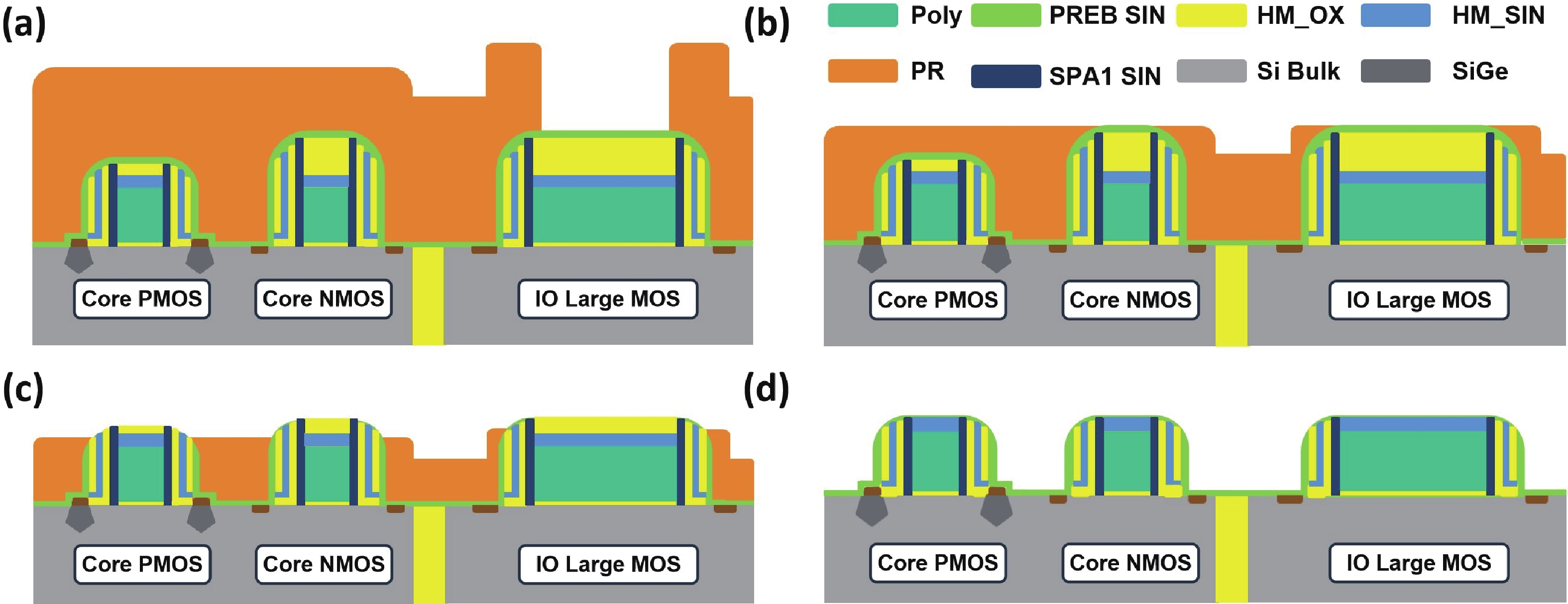
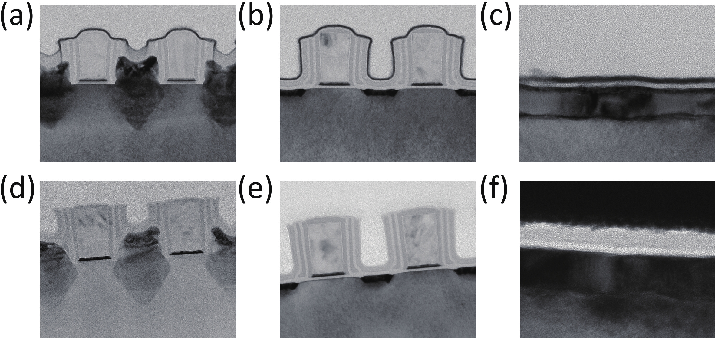
Fig. 1.
(Color online) Schematic of PREB process flow. (a) Photo exposure, (b) EB1 step, (c) EB2 ME step, (d) EB2 OE and Asher process.
ARTICLES
Ting Lei1, 2, Zhehong Liu2, Zhiwen Liu2, Guangjie Xue2, Chun Sun2, Jun Zhou2, and Xiangshui Miao1,
Corresponding author: Jun Zhou, Jerry_Zhou@xmcwh.com; Xiangshui Miao, miaoxs@hust.edu.cn
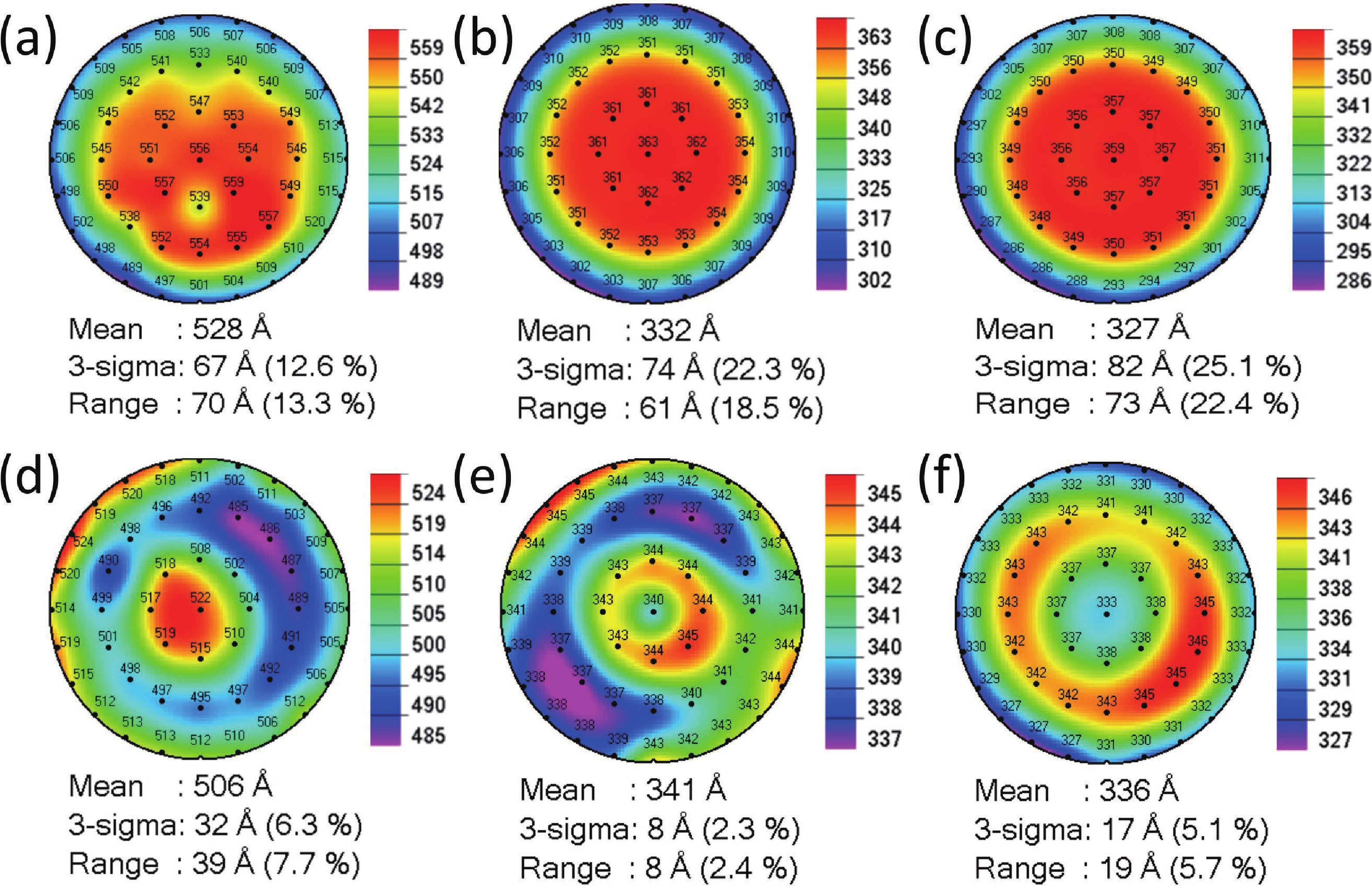
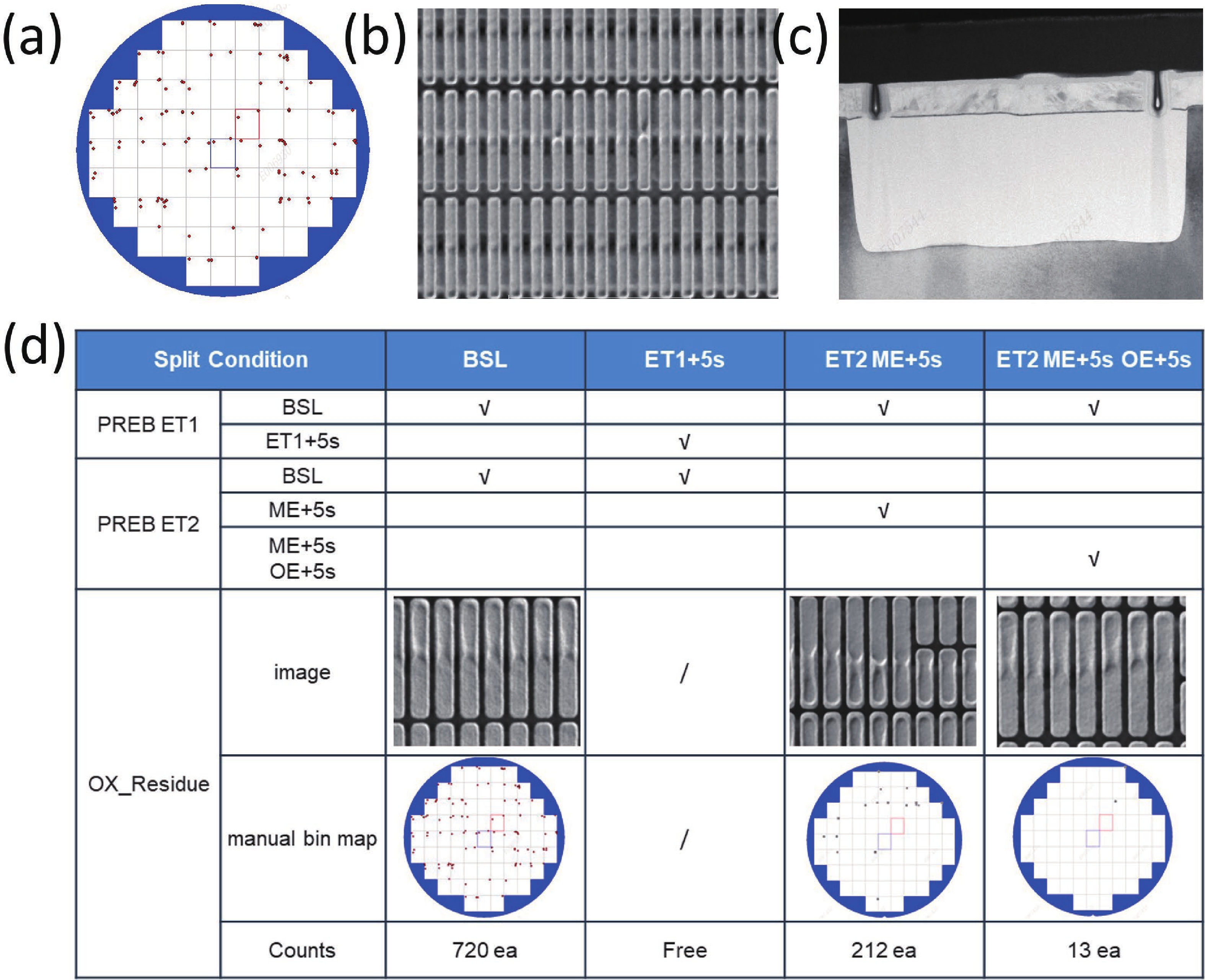
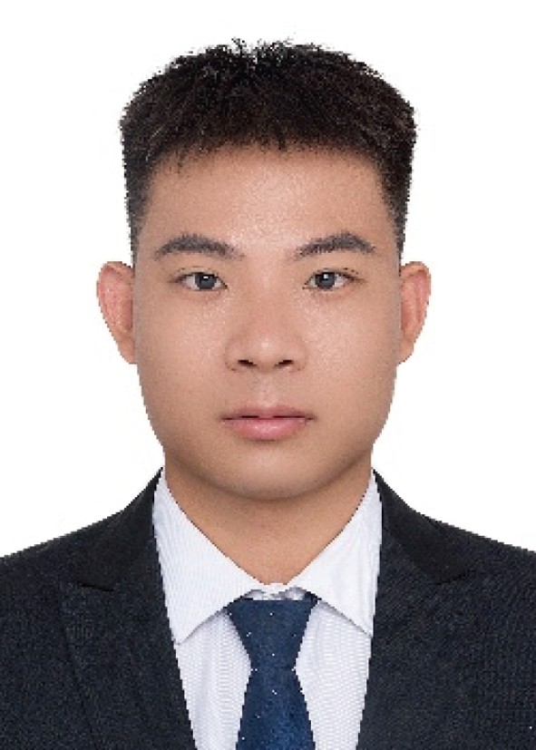
Abstract: The introduction of high-k/metal gate (HK/MG) technology enables independent tuning of N-type metal−oxide−semiconductor (NMOS) and P-type metal−oxide−semiconductor (PMOS) threshold voltages, facilitating advanced nodes and improving overall chip performance. However, severe pattern loading effects during PMOS device fabrication pose challenges in dummy poly removal. This work reports the optimization of the photoresist etch back (PREB) process, providing a wider process window for subsequent AL CMP. By tuning the PR coating uniformity to 1.6% and applying four-zone electrostatic chuck (ESC) temperature control, the wafer-level uniformities of PR, SiN, and SiO2 were reduced to 6.3%, 2.3%, and 5.1%, respectively. An optimized over etch (OE) recipe with a high selectivity of PR : SiN : SiO2 ≈ 1 : 1 : 6 effectively balanced gate height loading between N- and PMOS regions. Furthermore, precise EB1 time tuning enabled defect removal, while advanced KLA inspection ensured early detection of critical failure modes. Collectively, these measures establish a robust and stable PREB process for advanced logic device fabrication.
Keywords: PREB, dummy poly remove, horn height, pattern loading effect
| [1] |
Shao Q, Chen F, Jiang L, et al. High K metal gate CMP process development for 32 nm and beyond gate last approach. ECS Trans, 2013, 52(1): 523 doi: 10.1149/05201.0523ecst
|
| [2] |
Nunomura S, Morita Y. SiO2/Si interface defects in HKMG stack fabrication. Surf Interfaces, 2025, 56: 105445 doi: 10.1016/j.surfin.2024.105445
|
| [3] |
Li Z Y, Wang X J, Jiang Y L. Metal boundary effect mitigation by HKMG thermal process optimization in FinFET integration technology. IEEE Trans Electron Devices, 2024, 71(4): 2335 doi: 10.1109/TED.2024.3370119
|
| [4] |
Choi K M. 32 nm high K metal gate (HKMG) designs for low power applications. IEEE International SoC Design Conference, 2008, I
|
| [5] |
Trentzsch M, Flachowsky S, Richter R, et al. A 28nm HKMG super low power embedded NVM technology based on ferroelectric FETs. IEEE International Electron Devices Meeting, 2016: 1
|
| [6] |
Li C Y, Wang J J, Wang S H, et al. A review of IoT applications in healthcare. Neurocomputing, 2024, 565: 127017 doi: 10.1016/j.neucom.2023.127017
|
| [7] |
Alwahedi F, Aldhaheri A, Ferrag M A, et al. Machine learning techniques for IoT security: Current research and future vision with generative AI and large language models. Internet Things Cyber Phys Syst, 2024, 4: 167 doi: 10.1016/j.iotcps.2023.12.003
|
| [8] |
Ng D T K, Lee M, Tan R J Y, et al. A review of AI teaching and learning from 2000 to 2020. Educ Inf Technol, 2023, 28(7): 8445 doi: 10.1007/s10639-022-11491-w
|
| [9] |
Yu X F, Ai T T, Wang K. Application of nanogenerators in acoustics based on artificial intelligence and machine learning. APL Mater, 2024, 12(2): 020602 doi: 10.1063/5.0195399
|
| [10] |
Chih-Lin I, Han S F, Xu Z K, et al. 5G: Rethink mobile communications for 2020+. Philos Trans A Math Phys Eng Sci, 2016, 374(2062): 20140432
|
| [11] |
Chávez-Santiago R, Szydełko M, Kliks A, et al. 5G: The convergence of wireless communications. Wirel Pers Commun, 2015, 83(3): 1617 doi: 10.1007/s11277-015-2467-2
|
| [12] |
de Azevedo A M, Lopes T J, Cardoso D D, et al. SiGe semiconductor electronic component: a review on fundamentals and applications. Obs De La Econ Latinoam, 2024, 22(12): e8370
|
| [13] |
Beyer C, Bhattacharjee N, Mikolajick T, et al. Back-bias effects in a SiGe nanosheet transistor with multiple independent gates. Adv Mater Technol, 2025, 10(6): 2401391 doi: 10.1002/admt.202401391
|
| [14] |
Ji S L, Han Q H, Zhang H Y. Dummy poly gate removal scheme at FinFET. ECS Trans, 2017, 75(33): 15 doi: 10.1149/07533.0015ecst
|
| [15] |
Zeng Y Z, Zhao J, Gao H J, et al. Dummy poly removal impact factors and improvement in HKMG last process. ECS Trans, 2014, 60(1): 709 doi: 10.1149/06001.0709ecst
|
| [16] |
Huang S, Qu X F, Sun L, et al. N/P split boundary profile improvement in high K metal gate dummy poly remove process. 2022 China Semiconductor Technology International Conference (CSTIC), 2022: 1
|
| [17] |
Li J J, Pan H M, Yu M F, et al. An optimized monitoring method for 28 HK ILD CMP. 2022 China Semiconductor Technology International Conference (CSTIC), 2022: 1
|
| [18] |
Diao J, Leung G, Qian J, et al. ILD0 CMP: Technology enabler for high K metal gate in high performance logic devices. 2010 IEEE/SEMI Advanced Semiconductor Manufacturing Conference (ASMC), 2010: 247
|
| [19] |
Ma X, Wang K L, Yu J W, et al. Study on 28NM technology node ILD0-CMP Micro_Scratch defect reduction. 2024 Conference of Science and Technology for Integrated Circuits (CSTIC), 2024: 1
|
| [20] |
Que Y R, Ma X, Zhang J, et al. Study on the mechanism of SIN residue for ILD0 CMP. 2023 China Semiconductor Technology International Conference (CSTIC), 2023: 1
|
| [21] |
Li Y J, Zhang B C, Yang J G, et al. Study and optimization of photo resistor etch back loop in HK metal gate. 2022 China Semiconductor Technology International Conference (CSTIC), 2022: 1
|
| [22] |
Wang M, Chen H, Wang K, et al. The type and solution of inline poly residue defect for 28 HK process improvement. 2022 China Semiconductor Technology International Conference (CSTIC), 2022: 1
|
| [23] |
Song Y, Yang Z H, Tang X, et al. Study of PREB process in FDSOI. 2020 China Semiconductor Technology International Conference (CSTIC), 2020: 1
|


Article views: 1335 Times PDF downloads: 202 Times Cited by: 0 Times
Received: 16 July 2025 Revised: 18 September 2025 Online: Accepted Manuscript: 23 October 2025Uncorrected proof: 28 October 2025Published: 15 March 2026
| Citation: |
Ting Lei, Zhehong Liu, Zhiwen Liu, Guangjie Xue, Chun Sun, Jun Zhou, Xiangshui Miao. Optimization and defect control in photoresist etch back processes for advanced semiconductor technologies[J]. Journal of Semiconductors, 2026, 47(3): 032102. doi: 10.1088/1674-4926/25070024
****
T Lei, Z H Liu, Z W Liu, G J Xue, C Sun, J Zhou, and X S Miao, Optimization and defect control in photoresist etch back processes for advanced semiconductor technologies[J]. J. Semicond., 2026, 47(3): 032102 doi: 10.1088/1674-4926/25070024

|
 Ting Lei graduated with a Ph.D. from the University of Science and Technology of China (USTC) in 2023. He is currently a Senior Process Integration Engineer at Wuhan XinXin Semiconductor Manufacturing Co., Ltd., focusing on the research and development of advanced logic chips
 Jun Zhou got his bachelor’s degree in 2004 from Wuhan University of Technology and his master’s degree in 2014 from Wuhan University. He is currently the head of research and development in Wuhan XinXin Semiconductor Manufacturing Co., Ltd. His research focuses on advanced logic and non-volatile memory technology research
 Xiangshui Miao graduated from Huazhong University of Science and Technology (HUST) in 1996. He is currently the Dean of the School of Integrated Circuits at HUST. His research focuses on information storage materials and devices, including 3D phase-change memory, memristors, and brain-inspired computing and logic operations
| [1] |
Shao Q, Chen F, Jiang L, et al. High K metal gate CMP process development for 32 nm and beyond gate last approach. ECS Trans, 2013, 52(1): 523 doi: 10.1149/05201.0523ecst
|
| [2] |
Nunomura S, Morita Y. SiO2/Si interface defects in HKMG stack fabrication. Surf Interfaces, 2025, 56: 105445 doi: 10.1016/j.surfin.2024.105445
|
| [3] |
Li Z Y, Wang X J, Jiang Y L. Metal boundary effect mitigation by HKMG thermal process optimization in FinFET integration technology. IEEE Trans Electron Devices, 2024, 71(4): 2335 doi: 10.1109/TED.2024.3370119
|
| [4] |
Choi K M. 32 nm high K metal gate (HKMG) designs for low power applications. IEEE International SoC Design Conference, 2008, I
|
| [5] |
Trentzsch M, Flachowsky S, Richter R, et al. A 28nm HKMG super low power embedded NVM technology based on ferroelectric FETs. IEEE International Electron Devices Meeting, 2016: 1
|
| [6] |
Li C Y, Wang J J, Wang S H, et al. A review of IoT applications in healthcare. Neurocomputing, 2024, 565: 127017 doi: 10.1016/j.neucom.2023.127017
|
| [7] |
Alwahedi F, Aldhaheri A, Ferrag M A, et al. Machine learning techniques for IoT security: Current research and future vision with generative AI and large language models. Internet Things Cyber Phys Syst, 2024, 4: 167 doi: 10.1016/j.iotcps.2023.12.003
|
| [8] |
Ng D T K, Lee M, Tan R J Y, et al. A review of AI teaching and learning from 2000 to 2020. Educ Inf Technol, 2023, 28(7): 8445 doi: 10.1007/s10639-022-11491-w
|
| [9] |
Yu X F, Ai T T, Wang K. Application of nanogenerators in acoustics based on artificial intelligence and machine learning. APL Mater, 2024, 12(2): 020602 doi: 10.1063/5.0195399
|
| [10] |
Chih-Lin I, Han S F, Xu Z K, et al. 5G: Rethink mobile communications for 2020+. Philos Trans A Math Phys Eng Sci, 2016, 374(2062): 20140432
|
| [11] |
Chávez-Santiago R, Szydełko M, Kliks A, et al. 5G: The convergence of wireless communications. Wirel Pers Commun, 2015, 83(3): 1617 doi: 10.1007/s11277-015-2467-2
|
| [12] |
de Azevedo A M, Lopes T J, Cardoso D D, et al. SiGe semiconductor electronic component: a review on fundamentals and applications. Obs De La Econ Latinoam, 2024, 22(12): e8370
|
| [13] |
Beyer C, Bhattacharjee N, Mikolajick T, et al. Back-bias effects in a SiGe nanosheet transistor with multiple independent gates. Adv Mater Technol, 2025, 10(6): 2401391 doi: 10.1002/admt.202401391
|
| [14] |
Ji S L, Han Q H, Zhang H Y. Dummy poly gate removal scheme at FinFET. ECS Trans, 2017, 75(33): 15 doi: 10.1149/07533.0015ecst
|
| [15] |
Zeng Y Z, Zhao J, Gao H J, et al. Dummy poly removal impact factors and improvement in HKMG last process. ECS Trans, 2014, 60(1): 709 doi: 10.1149/06001.0709ecst
|
| [16] |
Huang S, Qu X F, Sun L, et al. N/P split boundary profile improvement in high K metal gate dummy poly remove process. 2022 China Semiconductor Technology International Conference (CSTIC), 2022: 1
|
| [17] |
Li J J, Pan H M, Yu M F, et al. An optimized monitoring method for 28 HK ILD CMP. 2022 China Semiconductor Technology International Conference (CSTIC), 2022: 1
|
| [18] |
Diao J, Leung G, Qian J, et al. ILD0 CMP: Technology enabler for high K metal gate in high performance logic devices. 2010 IEEE/SEMI Advanced Semiconductor Manufacturing Conference (ASMC), 2010: 247
|
| [19] |
Ma X, Wang K L, Yu J W, et al. Study on 28NM technology node ILD0-CMP Micro_Scratch defect reduction. 2024 Conference of Science and Technology for Integrated Circuits (CSTIC), 2024: 1
|
| [20] |
Que Y R, Ma X, Zhang J, et al. Study on the mechanism of SIN residue for ILD0 CMP. 2023 China Semiconductor Technology International Conference (CSTIC), 2023: 1
|
| [21] |
Li Y J, Zhang B C, Yang J G, et al. Study and optimization of photo resistor etch back loop in HK metal gate. 2022 China Semiconductor Technology International Conference (CSTIC), 2022: 1
|
| [22] |
Wang M, Chen H, Wang K, et al. The type and solution of inline poly residue defect for 28 HK process improvement. 2022 China Semiconductor Technology International Conference (CSTIC), 2022: 1
|
| [23] |
Song Y, Yang Z H, Tang X, et al. Study of PREB process in FDSOI. 2020 China Semiconductor Technology International Conference (CSTIC), 2020: 1
|
 Supporting_information.pdf
|

|

 WeChat ID
Journal of Semiconductors © 2017 All Rights Reserved 京ICP备05085259号-2

 DownLoad:

