| Citation: |
Zhipeng Liu, Yiling Hu, Zhi Liu, Jiashun Zhang, Jun Zheng, Xiaojie Yin, Yuhua Zuo, Junming An, Buwen Cheng. High-speed wavelength division multiplexing silicon photonics receiver chip based on silicon arrayed waveguide grating[J]. Journal of Semiconductors, 2026, 47(2): 022401. doi: 10.1088/1674-4926/25050018
****
Z P Liu, Y L Hu, Z Liu, J S Zhang, J Zheng, X J Yin, Y H Zuo, J M An, and B W Cheng, High-speed wavelength division multiplexing silicon photonics receiver chip based on silicon arrayed waveguide grating[J]. J. Semicond., 2026, 47(2): 022401 doi: 10.1088/1674-4926/25050018
|
High-speed wavelength division multiplexing silicon photonics receiver chip based on silicon arrayed waveguide grating
DOI: 10.1088/1674-4926/25050018
CSTR: 32376.14.1674-4926.25050018
More Information-
Abstract
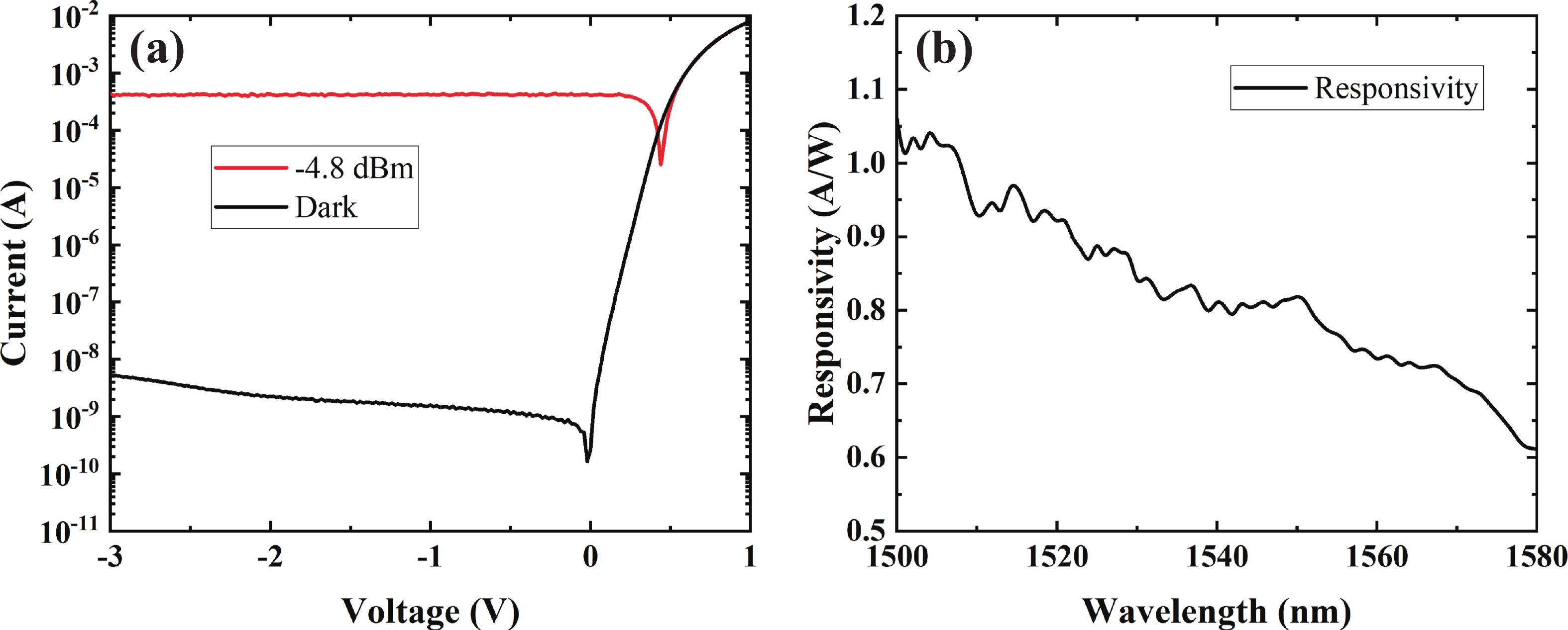
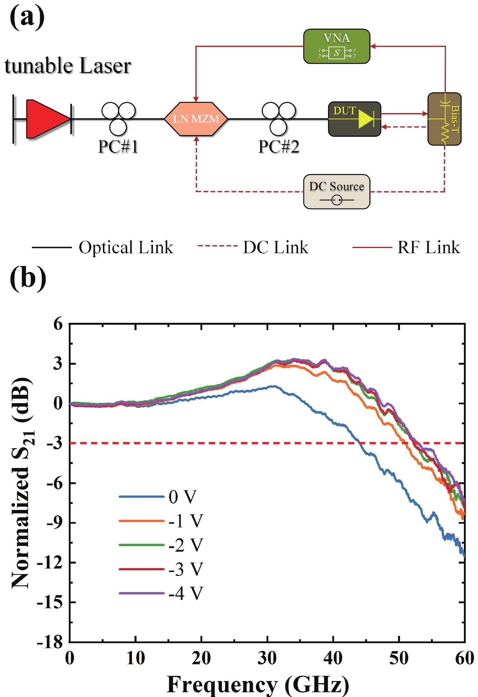
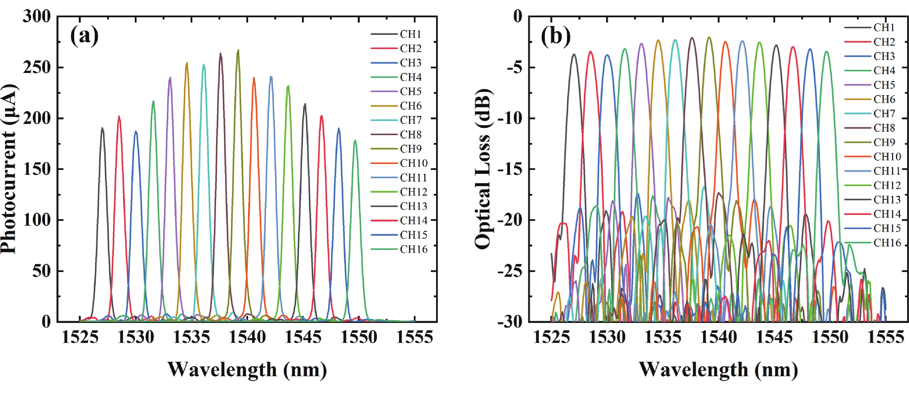
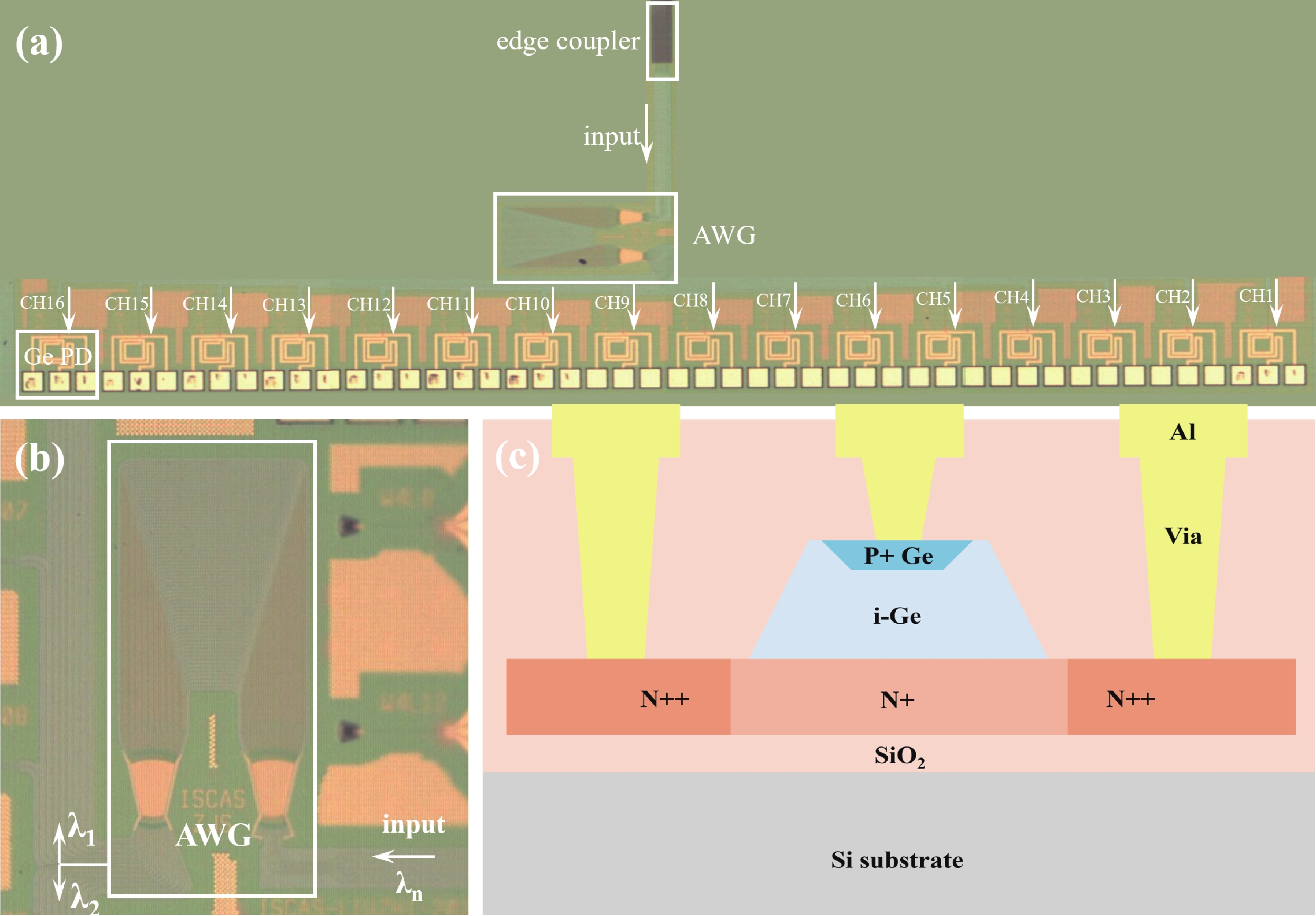
Wavelength division multiplexing technology has been pivotal in addressing the demand for high-capacity optical communication with silicon photonics providing a promising platform. This work presents a 16-channel wavelength division multiplexing silicon photonics receiver chip composed of an arrayed waveguide grating and Ge-on-Si photodetectors. Integrated inductors are introduced to enhance the high-speed performance of photodetectors, enabling data rates up to 112 Gbps with high responsivity and low dark current. The operating wavelength range of the arrayed wavelength grating is adjusted according to the response of the Ge-on-Si photodetector. The optical insertion loss, cross talk and central wavelength of the array waveguide grating are 2.1 to 3.7 dB, −12 to −15 dB, and 1538 nm, respectively. The proposed receiver chip offers a solution to meet the challenges of modern data transmission requirements.-
Keywords:
- silicon photonics,
- WDM,
- AWG,
- photodetector
-
References
[1] Shekhar S, Bogaerts W, Chrostowski L, et al. Roadmapping the next generation of silicon photonics. Nat Commun, 2024, 15(1): 751 doi: 10.1038/s41467-024-44750-0[2] Liu Z, Zhang J S, Li X L, et al. 25 × 50 Gbps wavelength division multiplexing silicon photonics receiver chip based on a silicon nanowire-arrayed waveguide grating. Photon Res, 2019, 7(6): 659 doi: 10.1364/PRJ.7.000659[3] Moralis-Pegios M, Mourgias-Alexandris G, Tsakyridis A, et al. Neuromorphic silicon photonics and hardware-aware deep learning for high-speed inference. J Light Technol, 2022, 40(10): 3243 doi: 10.1109/JLT.2022.3171831[4] He X Y, Guo P X, Sun W, et al. CPDM-PCNN: A compact and power efficient photonic convolutional neural network accelerator based on dual-function microring resonators. Opt Laser Technol, 2025, 188: 112889 doi: 10.1016/j.optlastec.2025.112889[5] Fang Z R, Chen R, Zheng J J, et al. Ultra-low-energy programmable non-volatile silicon photonics based on phase-change materials with graphene heaters. Nat Nanotechnol, 2022, 17(8): 842 doi: 10.1038/s41565-022-01153-w[6] Totovic A, Giamougiannis G, Tsakyridis A, et al. Programmable photonic neural networks combining WDM with coherent linear optics. Sci Rep, 2022, 12(1): 5605 doi: 10.1038/s41598-022-09370-y[7] Kabir M A, Taharat A, Keats A I, et al. High-performance demultiplexer-based lab-on-bio-chip sensor leveraging silicon photonics for point-of-care detection of hemoglobin and blood calcium ion levels. Opt Express, 2025, 33(9): 19788 doi: 10.1364/OE.554834[8] Kozdrowski S, Żotkiewicz M, Sujecki S. Ultra-wideband WDM optical network optimization. Photonics, 2020, 7(1): 16 doi: 10.3390/photonics7010016[9] Yoo S J B. Wavelength conversion technologies for WDM network applications. J Light Technol, 1996, 14(6): 955 doi: 10.1109/50.511595[10] Chen L, Doerr C R, Buhl L, et al. Monolithically integrated 40-wavelength demultiplexer and photodetector array on silicon. IEEE Photonics Technol Lett, 2011, 23(13): 869 doi: 10.1109/LPT.2011.2141128[11] Won R. Integrating silicon photonics. Nature Photon, 2010, 4(8): 498 doi: 10.1038/nphoton.2010.189[12] Fang Q, Liow T Y, Song J F, et al. WDM multi-channel silicon photonic receiver with 320 Gbps data transmission capability. Opt Express, 2010, 18(5): 5106 doi: 10.1364/OE.18.005106[13] Ye M Y, Li Y L, Zhang W L, et al. Multi-mode transmitter based on silicon microring modulators. IEEE Photonics J, 2022, 14(4): 6640504 doi: 10.1109/JPHOT.2022.3189438[14] Zhang Z, Li H, Huang B J, et al. Multi-channel silicon photonic receiver based on compact second-order microring resonators. Opt Commun, 2019, 437: 168 doi: 10.1016/j.optcom.2018.12.067[15] Feng D Z, Qian W, Liang H, et al. High-speed receiver technology on the SOI platform. IEEE J Sel Top Quantum Electron, 2013, 19(2): 3800108 doi: 10.1109/JSTQE.2012.2213804[16] Li K L, Zhang J S, An J M, et al. Design and fabrication of 25-channel 200 GHz AWG based on Si nanowire waveguides. Optoelectron Lett, 2017, 13(4): 241 doi: 10.1007/s11801-017-7076-8[17] Cui J L, Zheng J, Zhu Y P, et al. Sn component gradient GeSn photodetector with 3 dB bandwidth over 50 GHz for extending L band telecommunication. Opt Lett, 2023, 48(23): 6148 doi: 10.1364/OL.504190[18] Liu Z, Yang F, Wu W Z, et al. 48 GHz high-performance Ge-on-SOI photodetector with zero-bias 40 gbps grown by selective epitaxial growth. J Light Technol, 2017, 35(24): 5306 doi: 10.1109/JLT.2017.2766266[19] Li X L, Zhu Y P, Liu Z, et al. 75 GHz germanium waveguide photodetector with 64 Gbps data rates utilizing an inductive-gain-peaking technique. J Semicond, 2023, 44(1): 012301 doi: 10.1088/1674-4926/44/1/012301[20] Peng Y Y, Cao H Z, Xie J, et al. Silicon photonic transmitter and receiver for hybrid multiplexing systems. Chip, 2025, 4(4): 100148 doi: 10.1016/j.chip.2025.100148 -
Proportional views


 Zhipeng Liu received the B.S. degree from the University of Chinese Academy of Science, Beijing, China, in 2022. He is currently working toward the Ph.D. degree at the Institute of Semiconductors, Chinese Academy of Sciences, Beijing, China. His research interests include high-speed silicon-based photodetectors.
 Yiling Hu received the B.S. degree from Nankai University, Tianjin, China, in 2022. Now she is working toward the Ph.D. degree at the Institute of Semiconductors, Chinese Academy of Sciences, Beijing, China. Her research interests include high-speed silicon-based photodetectors and avalanche photodiodes.
 Zhi Liu received the Ph.D. degree from Institute of Semiconductors, Chinese Academy of Sciences, in 2014. Since 2014, he has been with the Institute of Semiconductors, Chinese Academy of Sciences. His research interests include silicon-based group Ⅳ material growth and silicon photonics.
 DownLoad:
