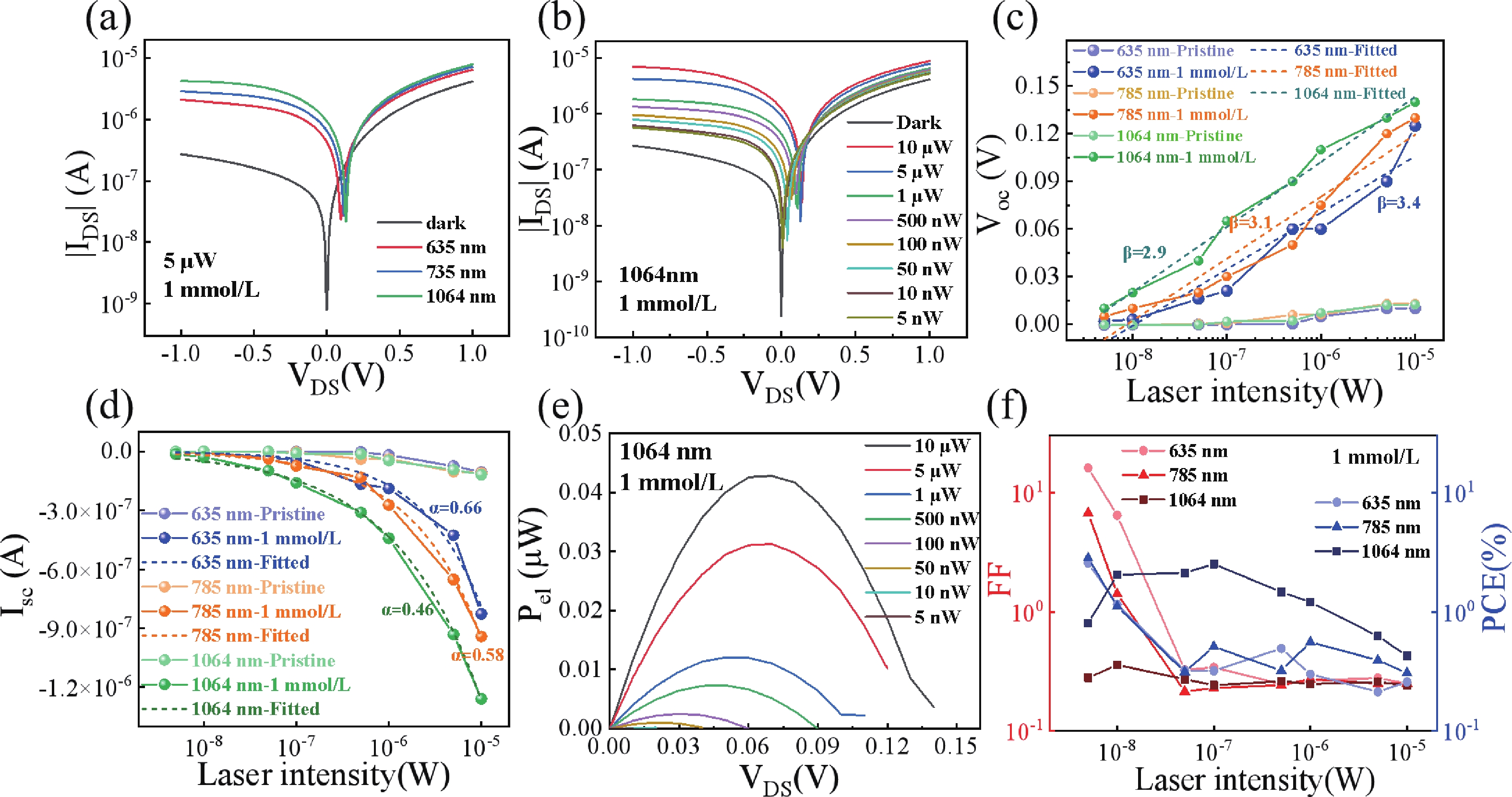
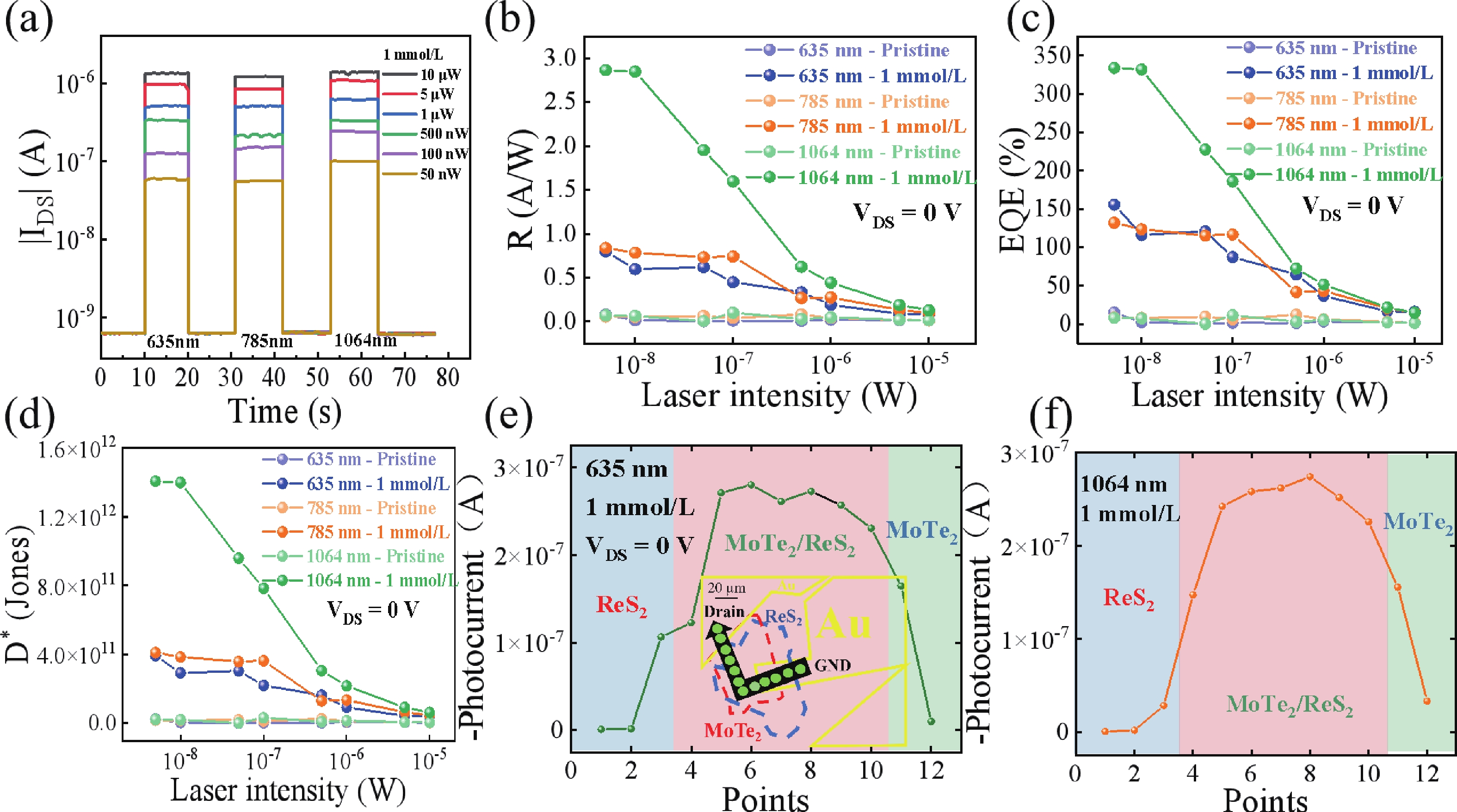
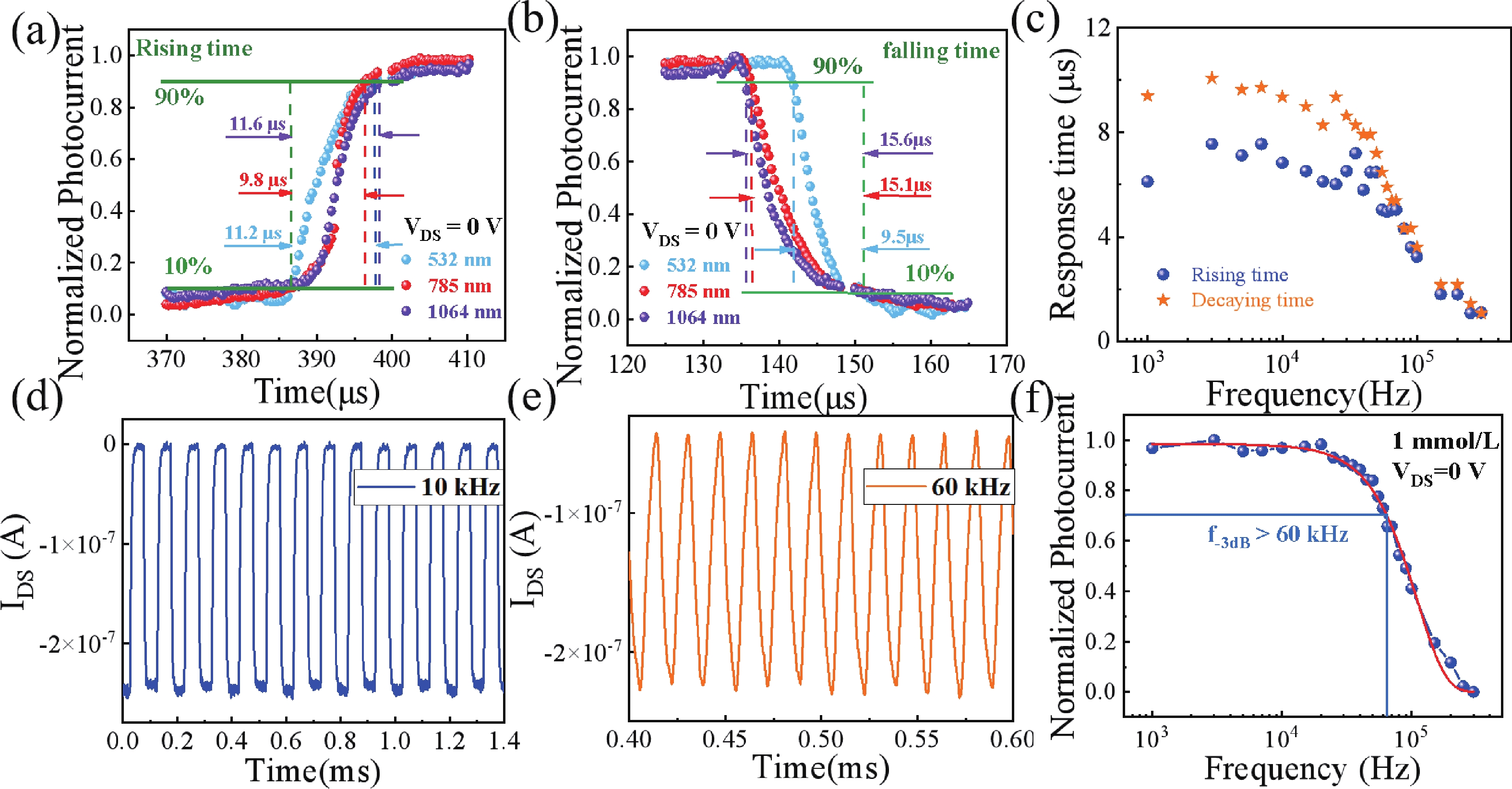
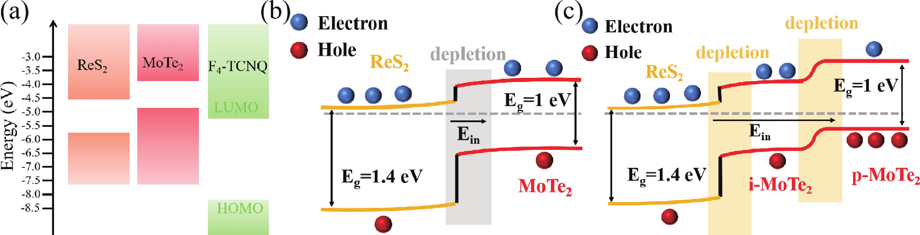
J. Semicond. >  Just Accepted

ARTICLES

Ultra-fast and high-responsivity self-powered vis-NIR photodetector via surface charge transfer doping in MoTe2/ReS2 heterostructures

Haozhe Ruan, Yongkang Liu, Jianyu Wang, Linjiang Xie, Yixuan Wang, Mengting Dong, Zhangting Wu and Liang Zheng

+ Author Affiliations

 Corresponding author: Zhangting Wu, wuzhangting@hdu.edu.cn; Liang Zheng, zhlbsbx@hdu.edu.cn

DOI: 10.1088/1674-4926/25060013CSTR: 32376.14.1674-4926.25060013

PDF

Turn off MathJax

Abstract: The development of optoelectronic technologies demands photodetectors with miniaturization, broadband operation, high sensitivity and low power consumption. Although 2D vdW heterostructures are promising candidates due to their built-in electric fields, ultrafast photocarrier separation, and tunable bandgaps, defect states limit their performance. Therefore, the modulation of the optoelectronic properties in such heterostructures is imperative. Surface charge transfer doping (SCTD) has emerged as a promising strategy for non-destructive modulation of electronic and optoelectronic characteristics in two-dimensional materials. In this work, we demonstrate the construction of high-performance p-i-n vertical heterojunction photodetectors through SCTD of MoTe2/ReS2 heterostructure using p-type F4-TCNQ. Systematic characterization reveals that the interfacial doping process effectively amplifies the built-in electric field, enhancing photogenerated carrier separation efficiency. Compared to the pristine heterojunction device, the doped photodetector exhibits remarkable visible to near-infrared (635−1064 nm) performance. Particularly under 1064 nm illumination at zero bias, the device achieves a responsivity of 2.86 A/W and specific detectivity of 1.41 × 10¹² Jones. Notably, the external quantum efficiency reaches an exceptional value of 334% compared to the initial 11.5%, while maintaining ultrafast response characteristics with rise/fall times of 11.6/15.6 μs. This work provides new insights into interface engineering through molecular doping for developing high-performance van der Waals optoelectronic devices.

Key words: MoTe2/ReS2 heterostructurebroadband photodetectorsurface charge transfer dopingp-i-n


[1]
Long M S, Wang P, Fang H H, et al. Progress, challenges, and opportunities for 2D material based photodetectors. Adv Funct Materials, 2019, 29(19), 1803807 doi: 10.1002/adfm.201803807
[2]
Huo N J, Konstantatos G. Recent progress and future prospects of 2D-based photodetectors. Adv Mater, 2018, 30(51), e1801164 doi: 10.1002/adma.201801164
[3]
Shao K W, Weng Z J, Nan H Y, et al. High-performance, broadband, and self-driven photodetector based on MoTe2 homojunction with asymmetrical contact interfaces. Appl Phys Lett, 2025, 126(9), 091904 doi: 10.1063/5.0254935
[4]
Duan S J, Zhao T G, et al. Controlled synthesis of Bi2O2Te nanosheets for high-performance broadband photodetectors. ACS Photonics, 2025, 12(6), 3198 doi: 10.1021/acsphotonics.5c00570
[5]
Wang Z, Tan C H, Peng M, et al. Giant infrared bulk photovoltaic effect in tellurene for broad-spectrum neuromodulation. Light Sci Appl, 2024, 13(1), 277 doi: 10.1038/s41377-024-01640-w
[6]
Liang S J, Cheng B, Cui X Y, et al. Van der waals heterostructures for high-performance device applications: Challenges and opportunities. Adv Mater, 2020, 32(27), 1903800 doi: 10.1002/adma.201903800
[7]
Qiao H, Huang Z Y, Ren X H, et al. Self-powered photodetectors based on 2D materials. Adv Opt Mater, 2020, 8, 1900765 doi: 10.1002/adom.201900765
[8]
Zhao T G, Guo J X, Li T T, et al. Substrate engineering for wafer-scale two-dimensional material growth: Strategies, mechanisms, and perspectives. Chem Soc Rev, 2023, 52(5), 1650 doi: 10.1039/D2CS00657J
[9]
Nourbakhsh A, Zubair A, Dresselhaus M S, et al. Transport properties of a MoS2/WSe2 heterojunction transistor and its potential for application. Nano Lett, 2016, 16(2), 1359 doi: 10.1021/acs.nanolett.5b04791
[10]
Lee G, Pearton S J, Ren F, et al. Two-dimensionally layered p-black phosphorus/n-MoS2/p-black phosphorus heterojunctions. ACS Appl Mater Interfaces, 2018, 10(12), 10347 doi: 10.1021/acsami.7b19334
[11]
Zhao H J, Wang Y F, Tang S Y, et al. Fast and high-responsivity MoS2/MoSe2 heterostructure photodetectors enabled by van der Waals contact interfaces. Appl Phys Lett, 2024, 125(3), 033102 doi: 10.1063/5.0218977
[12]
Zhao T G, Chen Y, Xu T F, et al. Topological insulator Bi2Se3 heterojunction with a low dark current for midwave infrared photodetection. ACS Photonics, 2024, 11(6), 2450 doi: 10.1021/acsphotonics.4c00347
[13]
Jiang Y R, Wang R Q, Li X P, et al. Photovoltaic field-effect photodiodes based on double van der waals heterojunctions. ACS Nano, 2021, 15(9), 14295 doi: 10.1021/acsnano.1c02830
[14]
Xu J P, Luo X G, Lin X, et al. Approaching the robust linearity in dual-floating van der waals photodiode. Adv Funct Materials, 2024, 34(12), 2310811 doi: 10.1002/adfm.202310811
[15]
Wang J, Liu C L, Zhang L B, et al. Selective enhancement of photoresponse with ferroelectric-controlled BP/In2Se3 vdW heterojunction. Adv Sci, 2023, 10(11), e2205813 doi: 10.1002/advs.202205813
[16]
Hu W N, Wang H, Dong J G, et al. Chemical dopant-free controlled MoTe2/MoSe2 heterostructure toward a self-driven photodetector and complementary logic circuits. ACS Appl Mater Interfaces, 2023, 15(14), 18182 doi: 10.1021/acsami.2c21785
[17]
Huo N J, Konstantatos G. Ultrasensitive all-2D MoS2 phototransistors enabled by an out-of-plane MoS2 PN homojunction. Nat Commun, 2017, 8, 572 doi: 10.1038/s41467-017-00722-1
[18]
Mouri S, Miyauchi Y, Matsuda K. Tunable photoluminescence of monolayer MoS2 via chemical doping. Nano Lett, 2013, 13(12), 5944 doi: 10.1021/nl403036h
[19]
Jo S H, Kang D H, Shim J, et al. A high-performance WSe2/h-BN photodetector using a triphenylphosphine (PPh3)-based n-doping technique. Adv Mater, 2016, 28(24), 4824 doi: 10.1002/adma.201600032
[20]
Jo S H, Park H Y, Kang D H, et al. Photodetectors: Broad detection range rhenium diselenide photodetector enhanced by (3-aminopropyl)triethoxysilane and triphenylphosphine treatment (adv. mater. 31/2016). Adv Mater, 2016, 28(31), 6518 doi: 10.1002/adma.201670212
[21]
Liu F C, Zheng S J, He X X, et al. Highly sensitive detection of polarized light using anisotropic 2D ReS2. Adv Funct Materials, 2016, 26(8), 1169 doi: 10.1002/adfm.201504546
[22]
Yamamoto M, Wang S T, Ni M Y, et al. Strong enhancement of Raman scattering from a bulk-inactive vibrational mode in few-layer MoTe2. ACS Nano, 2014, 8(4), 3895 doi: 10.1021/nn5007607
[23]
Kim J H, Bergren M R, Park J C, et al. Carrier multiplication in van der Waals layered transition metal dichalcogenides. Nat Commun, 2019, 10(1), 5488 doi: 10.1038/s41467-019-13325-9
[24]
Li Y Z, Pan J Y, Yan C X, et al. Efficient carrier multiplication in self-powered near-ultraviolet γ-InSe/graphene heterostructure photodetector with external quantum efficiency exceeding 161. Nano Lett, 2024
[25]
Ma P, Flöry N, Salamin Y, et al. Fast MoTe2 waveguide photodetector with high sensitivity at telecommunication wavelengths. ACS Photonics, 2018, 5(5), 1846 doi: 10.1021/acsphotonics.8b00068
[26]
Zhao D Y, Chen Y, Jiang W, et al. Gate-tunable photodiodes based on mixed-dimensional Te/MoTe2 van der waals heterojunctions. Adv Elect Materials, 2021, 7(5), 2001066 doi: 10.1002/aelm.202001066
[27]
Chen Y, Wang X D, Wu G J, et al. High-performance photovoltaic detector based on MoTe2/MoS2 van der waals heterostructure. Small, 2018, 14(9
[28]
Chen J, Shan Y, Wang Q, et al. P-type laser-doped WSe2/MoTe2 van der Waals heterostructure photodetector. Nanotechnology, 2020, 31(29), 295201 doi: 10.1088/1361-6528/ab87cd
[29]
Luo H, Wang B L, Wang E Z, et al. High-responsivity photovoltaic photodetectors based on MoTe2/MoSe2 van der waals heterojunctions. Crystals, 2019, 9(6), 315 doi: 10.3390/cryst9060315
[30]
Varghese A, Saha D, Thakar K, et al. Near-direct bandgap WSe2/ReS2 type-II pn heterojunction for enhanced ultrafast photodetection and high-performance photovoltaics. Nano Lett, 2020, 20(3), 1707 doi: 10.1021/acs.nanolett.9b04879
[31]
Lezama I G, Ubaldini A, Longobardi M, et al. Surface transport and band gap structure of exfoliated 2H-MoTe2 crystals. 2D Mater, 2014, 1(2), 021002 doi: 10.1088/2053-1583/1/2/021002
Fig. 1.  (Color online) (a) Optical microscope image of the semi-vertical MoTe2/ReS2 photodetector. (b) Surface potential image of the MoTe2/ReS2 heterojunction; Potential line profile along the green dashed line. (c) Raman spectra of individual MoTe2 and ReS2 multilayers, as well as the overlapping heterojunction region. (d) Schematic diagram of the semi-vertical MoTe2/ReS2 photodetector after surface doping. (e) Output curves (VGS=0 V) of MoTe2/ReS2 photodetector before and after doping. (f)Transfer curves (VDS=1 V) of MoTe2 and ReS2 devices before and after doping. (g) Output curves of MoTe2 FET with sandwich-like structure in dark before and after doping. (h) Temporal photoresponse of undoped and doped MoTe2 FET with sandwich-like structure. (i) Carrier distribution in the vertical p-n MoTe2 junction formed by F4-TCNQ doping.

Fig. 2.  (Color online) (a) Output curves of the doped MoTe2/ReS2 photodetector under laser irradiation at different wavelengths. (b) Output curves of the doped photodetector under 1064 nm laser irradiation with varying optical power level. (c, d) VOC and ISC of MoTe2/ReS2 photodetector under 635, 785, and 1064 nm laser irradiation before and after doping. (e) Electrical power Pel versus bias voltage characteristics extracted from the doped photodetector under 1064 nm illumination with different optical power densities. (f) Fill factor FF and power conversion efficiency PCE of the doped photodetector as a function of irradiation power for lasers at 635, 785, 1064 nm.

Fig. 3.  (Color online) (a) Temporal photovoltaic response of the MoTe2/ReS2 photodetector under 1mmol/L F4-TCNQ doping. (b−d) Responsivity, external quantum efficiency, and specific detectivity across 635, 785, and 1064 nm wavelengths. (e, f) Spatial photocurrent line scans of the doped heterojunction at VDS = 0 V under 635 (e) and 1064 nm (f) laser illumination. The green-marked point indicates the laser focus position, with the scan direction denoted by the black arrow in the inset of (e).

Fig. 4.  (Color online) (a,b) Rise and fall times of the doped photodetectors under laser irradiation at varied wavelengths. (c) Dependence of rise/fall times on switching frequency under 532 nm illumination. (d,e) Reproducible photocurrent switching dynamics at 532 nm with modulation frequencies of 10 and 60 kHz. (f) Frequency-dependent normalized photocurrent.

Fig. 5.  (Color online) (a) Energy band structure diagrams of MoTe2, ReS2, and F4-TCNQ molecules before contact. (b) Energy band diagrams of MoTe2/ReS2 heterojunction at equilibrium after contact. (c) Energy band diagrams of p-i-n photodetector after doping.

Table 1.   Comparison of the photoresponse of the devices in this work with previously reported photodetectors.

ReferencesDevicesRise/fall timeResponsivityWavelength
This workF4-TCNQ/MoTe2/ReS210.44/11.8 µs2.86 A/W1064 nm
This workMoTe2/ReS27.1/8.1 µs0.099 A/W1064 nm
[25]MoTe223 mA/W1310 nm
[26]Te/MoTe28.1/29.8 ms0.11 mA/W1310 nm
[27]MoTe2/MoS260/25 µs43.6 mA/W637 nm
[28]WSe2 /MoTe272 µs1.8 mA/W633 nm
[29]MoTe2/MoSe230/35 ms1.5 A/WWhite light
DownLoad: CSV
[1]
Long M S, Wang P, Fang H H, et al. Progress, challenges, and opportunities for 2D material based photodetectors. Adv Funct Materials, 2019, 29(19), 1803807 doi: 10.1002/adfm.201803807
[2]
Huo N J, Konstantatos G. Recent progress and future prospects of 2D-based photodetectors. Adv Mater, 2018, 30(51), e1801164 doi: 10.1002/adma.201801164
[3]
Shao K W, Weng Z J, Nan H Y, et al. High-performance, broadband, and self-driven photodetector based on MoTe2 homojunction with asymmetrical contact interfaces. Appl Phys Lett, 2025, 126(9), 091904 doi: 10.1063/5.0254935
[4]
Duan S J, Zhao T G, et al. Controlled synthesis of Bi2O2Te nanosheets for high-performance broadband photodetectors. ACS Photonics, 2025, 12(6), 3198 doi: 10.1021/acsphotonics.5c00570
[5]
Wang Z, Tan C H, Peng M, et al. Giant infrared bulk photovoltaic effect in tellurene for broad-spectrum neuromodulation. Light Sci Appl, 2024, 13(1), 277 doi: 10.1038/s41377-024-01640-w
[6]
Liang S J, Cheng B, Cui X Y, et al. Van der waals heterostructures for high-performance device applications: Challenges and opportunities. Adv Mater, 2020, 32(27), 1903800 doi: 10.1002/adma.201903800
[7]
Qiao H, Huang Z Y, Ren X H, et al. Self-powered photodetectors based on 2D materials. Adv Opt Mater, 2020, 8, 1900765 doi: 10.1002/adom.201900765
[8]
Zhao T G, Guo J X, Li T T, et al. Substrate engineering for wafer-scale two-dimensional material growth: Strategies, mechanisms, and perspectives. Chem Soc Rev, 2023, 52(5), 1650 doi: 10.1039/D2CS00657J
[9]
Nourbakhsh A, Zubair A, Dresselhaus M S, et al. Transport properties of a MoS2/WSe2 heterojunction transistor and its potential for application. Nano Lett, 2016, 16(2), 1359 doi: 10.1021/acs.nanolett.5b04791
[10]
Lee G, Pearton S J, Ren F, et al. Two-dimensionally layered p-black phosphorus/n-MoS2/p-black phosphorus heterojunctions. ACS Appl Mater Interfaces, 2018, 10(12), 10347 doi: 10.1021/acsami.7b19334
[11]
Zhao H J, Wang Y F, Tang S Y, et al. Fast and high-responsivity MoS2/MoSe2 heterostructure photodetectors enabled by van der Waals contact interfaces. Appl Phys Lett, 2024, 125(3), 033102 doi: 10.1063/5.0218977
[12]
Zhao T G, Chen Y, Xu T F, et al. Topological insulator Bi2Se3 heterojunction with a low dark current for midwave infrared photodetection. ACS Photonics, 2024, 11(6), 2450 doi: 10.1021/acsphotonics.4c00347
[13]
Jiang Y R, Wang R Q, Li X P, et al. Photovoltaic field-effect photodiodes based on double van der waals heterojunctions. ACS Nano, 2021, 15(9), 14295 doi: 10.1021/acsnano.1c02830
[14]
Xu J P, Luo X G, Lin X, et al. Approaching the robust linearity in dual-floating van der waals photodiode. Adv Funct Materials, 2024, 34(12), 2310811 doi: 10.1002/adfm.202310811
[15]
Wang J, Liu C L, Zhang L B, et al. Selective enhancement of photoresponse with ferroelectric-controlled BP/In2Se3 vdW heterojunction. Adv Sci, 2023, 10(11), e2205813 doi: 10.1002/advs.202205813
[16]
Hu W N, Wang H, Dong J G, et al. Chemical dopant-free controlled MoTe2/MoSe2 heterostructure toward a self-driven photodetector and complementary logic circuits. ACS Appl Mater Interfaces, 2023, 15(14), 18182 doi: 10.1021/acsami.2c21785
[17]
Huo N J, Konstantatos G. Ultrasensitive all-2D MoS2 phototransistors enabled by an out-of-plane MoS2 PN homojunction. Nat Commun, 2017, 8, 572 doi: 10.1038/s41467-017-00722-1
[18]
Mouri S, Miyauchi Y, Matsuda K. Tunable photoluminescence of monolayer MoS2 via chemical doping. Nano Lett, 2013, 13(12), 5944 doi: 10.1021/nl403036h
[19]
Jo S H, Kang D H, Shim J, et al. A high-performance WSe2/h-BN photodetector using a triphenylphosphine (PPh3)-based n-doping technique. Adv Mater, 2016, 28(24), 4824 doi: 10.1002/adma.201600032
[20]
Jo S H, Park H Y, Kang D H, et al. Photodetectors: Broad detection range rhenium diselenide photodetector enhanced by (3-aminopropyl)triethoxysilane and triphenylphosphine treatment (adv. mater. 31/2016). Adv Mater, 2016, 28(31), 6518 doi: 10.1002/adma.201670212
[21]
Liu F C, Zheng S J, He X X, et al. Highly sensitive detection of polarized light using anisotropic 2D ReS2. Adv Funct Materials, 2016, 26(8), 1169 doi: 10.1002/adfm.201504546
[22]
Yamamoto M, Wang S T, Ni M Y, et al. Strong enhancement of Raman scattering from a bulk-inactive vibrational mode in few-layer MoTe2. ACS Nano, 2014, 8(4), 3895 doi: 10.1021/nn5007607
[23]
Kim J H, Bergren M R, Park J C, et al. Carrier multiplication in van der Waals layered transition metal dichalcogenides. Nat Commun, 2019, 10(1), 5488 doi: 10.1038/s41467-019-13325-9
[24]
Li Y Z, Pan J Y, Yan C X, et al. Efficient carrier multiplication in self-powered near-ultraviolet γ-InSe/graphene heterostructure photodetector with external quantum efficiency exceeding 161. Nano Lett, 2024
[25]
Ma P, Flöry N, Salamin Y, et al. Fast MoTe2 waveguide photodetector with high sensitivity at telecommunication wavelengths. ACS Photonics, 2018, 5(5), 1846 doi: 10.1021/acsphotonics.8b00068
[26]
Zhao D Y, Chen Y, Jiang W, et al. Gate-tunable photodiodes based on mixed-dimensional Te/MoTe2 van der waals heterojunctions. Adv Elect Materials, 2021, 7(5), 2001066 doi: 10.1002/aelm.202001066
[27]
Chen Y, Wang X D, Wu G J, et al. High-performance photovoltaic detector based on MoTe2/MoS2 van der waals heterostructure. Small, 2018, 14(9
[28]
Chen J, Shan Y, Wang Q, et al. P-type laser-doped WSe2/MoTe2 van der Waals heterostructure photodetector. Nanotechnology, 2020, 31(29), 295201 doi: 10.1088/1361-6528/ab87cd
[29]
Luo H, Wang B L, Wang E Z, et al. High-responsivity photovoltaic photodetectors based on MoTe2/MoSe2 van der waals heterojunctions. Crystals, 2019, 9(6), 315 doi: 10.3390/cryst9060315
[30]
Varghese A, Saha D, Thakar K, et al. Near-direct bandgap WSe2/ReS2 type-II pn heterojunction for enhanced ultrafast photodetection and high-performance photovoltaics. Nano Lett, 2020, 20(3), 1707 doi: 10.1021/acs.nanolett.9b04879
[31]
Lezama I G, Ubaldini A, Longobardi M, et al. Surface transport and band gap structure of exfoliated 2H-MoTe2 crystals. 2D Mater, 2014, 1(2), 021002 doi: 10.1088/2053-1583/1/2/021002

Supplementary_Materials.pdf

  • Search

    Advanced Search >>

    GET CITATION

    shu

    Export: BibTex EndNote

    Article Metrics

    Article views: 22 Times PDF downloads: 2 Times Cited by: 0 Times

    History

    Received: 10 June 2025 Revised: 20 July 2025 Online: Accepted Manuscript: 18 September 2025

    Catalog

      Email This Article

      User name:
      Email:*请输入正确邮箱
      Code:*验证码错误
      Haozhe Ruan, Yongkang Liu, Jianyu Wang, Linjiang Xie, Yixuan Wang, Mengting Dong, Zhangting Wu, Liang Zheng. Ultra-fast and high-responsivity self-powered vis-NIR photodetector via surface charge transfer doping in MoTe2/ReS2 heterostructures[J]. Journal of Semiconductors, 2025, In Press. doi: 10.1088/1674-4926/25060013 ****H Z Ruan, Y K Liu, J Y Wang, L J Xie, Y X Wang, M T Dong, Z T Wu, and L Zheng, Ultra-fast and high-responsivity self-powered vis-NIR photodetector via surface charge transfer doping in MoTe2/ReS2 heterostructures[J]. J. Semicond., 2025, accepted doi: 10.1088/1674-4926/25060013
      Citation:
      Haozhe Ruan, Yongkang Liu, Jianyu Wang, Linjiang Xie, Yixuan Wang, Mengting Dong, Zhangting Wu, Liang Zheng. Ultra-fast and high-responsivity self-powered vis-NIR photodetector via surface charge transfer doping in MoTe2/ReS2 heterostructures[J]. Journal of Semiconductors, 2025, In Press. doi: 10.1088/1674-4926/25060013 ****
      H Z Ruan, Y K Liu, J Y Wang, L J Xie, Y X Wang, M T Dong, Z T Wu, and L Zheng, Ultra-fast and high-responsivity self-powered vis-NIR photodetector via surface charge transfer doping in MoTe2/ReS2 heterostructures[J]. J. Semicond., 2025, accepted doi: 10.1088/1674-4926/25060013

      Ultra-fast and high-responsivity self-powered vis-NIR photodetector via surface charge transfer doping in MoTe2/ReS2 heterostructures

      DOI: 10.1088/1674-4926/25060013
      CSTR: 32376.14.1674-4926.25060013
      More Information
      • Haozhe Ruan received his bachelor’s degree in 2024 from Hangzhou Dianzi University. Now he is a graduate student at Hangzhou Dianzi University under the supervision of Prof. Zhangting Wu. His research focuses on two-dimensional vertical heterojunction photodetectors
      • Zhangting Wu, Associate Professor at the School of Electronics and Information Engineering, Hangzhou Dianzi University (HDU), specializes in electrical/optoelectronic properties of 2D materials and heterostructures. She earned her Ph.D. from Southeast University (2017), joined HDU in 2018, and was a Visiting Scholar at Zhejiang University (2024-2025). Supported by grants from the National Natural Science Foundation of China (NSFC) and Zhejiang Provincial Natural Science Foundation, she has published multiple first/corresponding-author papers in journals including ACS Nano, Nano Research, ACS Appl. Mater. Interfaces, Chem. Soc. Rev., and Nanophotonics
      • Liang Zheng, Professor and PhD Supervisor at Hangzhou Dianzi University (HDU), held successive roles as Department Head (Electronic Science & Technology, 2013-2019), Deputy Director (Advanced Technology Institute, 2019-2023), and currently as Deputy Director of Personnel Office (since 2023). He secured projects including a National Key R&D sub-project, NSFC grant, ZBFZB key initiative, two Zhejiang NSF grants, two public welfare projects, and a Young Talent Program; co-directed two defense projects (GF Pre-research, JWKJW Innovation Zone); authored >60 SCI papers. His research spans field-induced electron emission, power device packaging/thermal management, sensor fault diagnosis, and EMI suppression
      • Corresponding author: wuzhangting@hdu.edu.cnzhlbsbx@hdu.edu.cn
      • Received Date: 2025-06-10
      • Revised Date: 2025-07-20
      • Available Online: 2025-09-18

      Catalog

        /

        DownLoad:  Full-Size Img  PowerPoint
        Return
        Return