


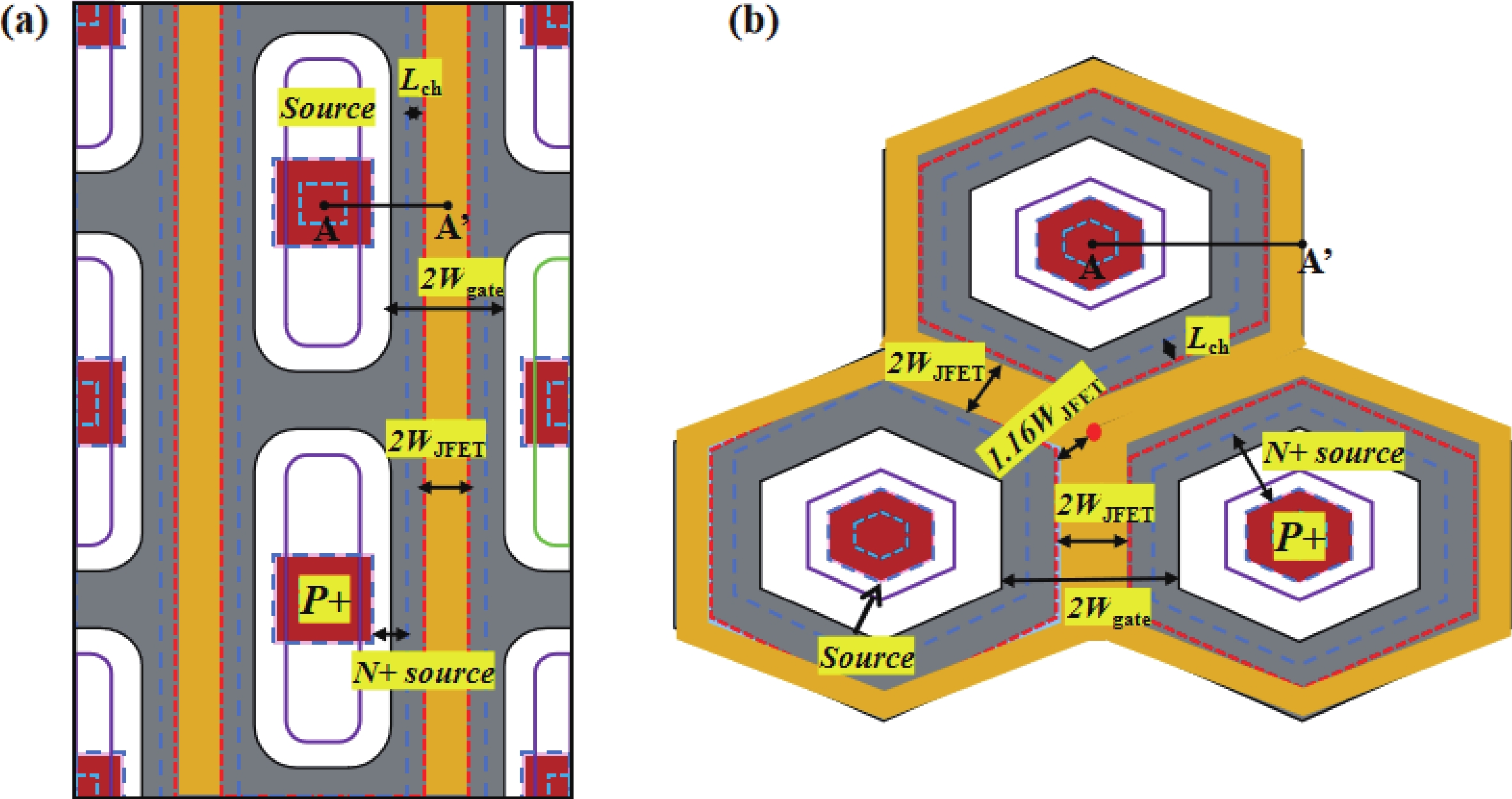
Fig. 1.
(Color online) (a) Linear layout topology and (b) hexagonal layout topology of the 4H-SiC MOSFET.
ARTICLES
Bofeng Zheng1, Houcai Luo1, Huan Wu1, Jingping Zhang1 and Xianping Chen1, 2,
Corresponding author: Xianping Chen, xianpingchen@cqu.edu.cn
Abstract: High gate oxide electric field, which can lead to device failure, is a common issue in SiC MOSFETs. To mitigate this issue and ensure high device reliability, an electric field shielding layer (also called depletion layer) in JFET region is always used to reduce the gate oxide electric filed strength (Eox,max). However, there is still a lack of a detection methods to characterize the changes in the depletion layer of the JFET region. In this paper, a type of 1200 V 4H-SiC MOSFET with different JFET widths and cell topologies is designed and fabricated, and an innovative detection method for the depletion layer of JFET region is proposed for the first time. This method is adopted to focus on discussing the influence of the depletion layer formed by different JFET widths on Vg, and the changes in the gate oxide capacitance Cg of hexagonal cells and linear cells during the formation of the JFET depletion layer are studied. Finally, the robustness of different cell topologies and JFET widths is determined by the depletion voltage drift in the high temperature gate reverse bias tests (HTGB−) reliability test.
Keywords: 4H-SiC, depletion layer, gate oxide capacitance, JFET region, reliability
| [1] |
Weitzel C E, Palmour J W, Carter C H, et al. Silicon carbide high-power devices. IEEE Trans Electron Devices, 1996, 43(10): 1732 doi: 10.1109/16.536819
|
| [2] |
Callanan R J, Agarwal A, Burk A, et al. Recent progress in SiC DMOSFETs and JBS diodes at cree. 2008 34th Annual Conference of IEEE Industrial Electronics, 2008: 2885 doi: 10.1109/IECON.2008.4758417
|
| [3] |
Rupp R. CoolSiC™ and major trends in SiC power device development. 2017 47th European Solid-State Device Research Conference (ESSDERC), 2017: 118 doi: 10.1109/ESSDERC.2017.8066606
|
| [4] |
Millán J, Godignon P, Perpiñà X, et al. A survey of wide bandgap power semiconductor devices. IEEE Trans Power Electron, 2014, 29(5): 2155 doi: 10.1109/TPEL.2013.2268900
|
| [5] |
Ostling M, Ghandi R, Zetterling C M. SiC power devices—Present status, applications and future perspective. 2011 IEEE 23rd International Symposium on Power Semiconductor Devices and ICs, 2011: 10 doi: 10.1109/ISPSD.2011.5890778
|
| [6] |
A Khan, A Imran, M Hasan. A 2.25kV, 6.1mΩ-cm2 4H-SiC normally-off VJFET. 2012 2nd International Conference on Power, Control and Embedded Systems, 2012: 1 doi: 10.1109/ICPCES.2012.6508119
|
| [7] |
Afanas’ev V V, Stesmans A, Bassler M, et al. Shallow electron traps at the 4H–SiC/SiO2 interface. Appl Phys Lett, 2000, 76(3): 336 doi: 10.1063/1.125737
|
| [8] |
Chung G Y, Tin C C, Williams J R, et al. Improved inversion channel mobility for 4H-SiC MOSFETs following high temperature anneals in nitric oxide. IEEE Electron Device Lett, 2001, 22(4): 176 doi: 10.1109/55.915604
|
| [9] |
Kong M F, Hou Y R, Yi B, et al. A high speed high voltage normally-off SiC vertical JFET power device. 2019 IEEE International Conference on Electron Devices and Solid-State Circuits (EDSSC), 2019: 1 doi: 10.1109/EDSSC.2019.8754097
|
| [10] |
Treu M, Rupp R, Blaschitz P, et al. Strategic considerations for unipolar SiC switch options: JFET vs. MOSFET. 2007 IEEE Industry Applications Annual Meeting, 2007: 324 doi: 10.1109/07IAS.2007.10
|
| [11] |
Zhou W C, Zhong X Q, Sheng K. High temperature stability and the performance degradation of SiC MOSFETs. IEEE Trans Power Electron, 2014, 29(5): 2329 doi: 10.1109/TPEL.2013.2283509
|
| [12] |
Ji S Q, Zheng S, Wang F, et al. Temperature-dependent characterization, modeling, and switching speed-limitation analysis of third-generation 10-kV SiC MOSFET. IEEE Trans Power Electron, 2018, 33(5): 4317 doi: 10.1109/TPEL.2017.2723601
|
| [13] |
Gonzalez J O, Alatise O, Hu J, et al. An investigation of temperature-sensitive electrical parameters for SiC power MOSFETs. IEEE Trans Power Electron, 2017, 32(10): 7954 doi: 10.1109/TPEL.2016.2631447
|
| [14] |
Soler V, Cabello M, Montserrat J, et al. 4.5kV SiC MOSFET with boron doped gate dielectric. 2016 28th International Symposium on Power Semiconductor Devices and ICs (ISPSD), 2016: 283 doi: 10.1109/ISPSD.2016.7520833
|
| [15] |
Noguchi M, Iwamatsu T, Amishiro H, et al. Determination of intrinsic phonon-limited mobility and carrier transport property extraction of 4H-SiC MOSFETs. 2017 IEEE International Electron Devices Meeting (IEDM), 2017: 9.3.1 doi: 10.1109/IEDM.2017.8268358
|
| [16] |
Deboy G, Treu M, Haeberlen O, et al. Si, SiC and GaN power devices: An unbiased view on key performance indicators. 2016 IEEE International Electron Devices Meeting (IEDM), 2016: 20.2.1 doi: 10.1109/IEDM.2016.7838458
|
| [17] |
Wu H, Luo H C, Zhang J P, et al. Investigation of unclamped inductive switch characteristics in 4H-SiC MOSFETs with different cell topologies. IEEE Trans Electron Devices, 2023, 70(3): 1181 doi: 10.1109/TED.2022.3233816
|
| [18] |
Kitai H, Hozumi Y, Shiomi H, et al. Low on-resistance and fast switching of 13-kV SiC MOSFETs with optimized junction field-effect transistor region. 2017 29th International Symposium on Power Semiconductor Devices and IC’s (ISPSD), 2017: 343 doi: 10.23919/ISPSD.2017.7988982
|
| [19] |
Sung W, Han K, Baliga B J. Optimization of the JFET region of 1.2kV SiC MOSFETs for improved high frequency figure of merit (HF-FOM). 2017 IEEE 5th Workshop on Wide Bandgap Power Devices and Applications (WiPDA), 2017: 238 doi: 10.1109/WiPDA.2017.8170553
|
| [20] |
Zhu S N, Liu T S, Fan J C, et al. A new cell topology for 4H-SiC planar power MOSFETs for high-frequency switching. Materials, 2022, 15(19): 6690 doi: 10.3390/ma15196690
|
| [21] |
Losee P A, Bolotnikov A, Yu L C, et al. SiC MOSFET design considerations for reliable high voltage operation. 2017 IEEE International Reliability Physics Symposium (IRPS), 2017: 2A doi: 10.1109/IRPS.2017.7936254
|
| [22] |
Donato N, Naydenov K, Udrea F, et al. On the short circuit electro-thermal failure of 1.2 kV 4H-SiC MOSFETs with 3D cell layouts. Mater Sci Forum, 2022, 1062: 632 doi: 10.4028/p-fnekfr
|
| [23] |
Agarwal A, Han K, Baliga B J. Impact of cell topology on characteristics of 600V 4H-SiC planar MOSFETs. IEEE Electron Device Lett, 2019, 40(5): 773 doi: 10.1109/LED.2019.2908078
|
| [24] |
Naydenov K, Donato N, Udrea F, et al. Clamped and unclamped inductive switching of 3.3 kV 4H-SiC MOSFETs with 3D cellular layouts. Mater Sci Forum, 2022, 1062: 627 doi: 10.4028/p-s1v84y
|
| [25] |
Wu H, Luo H C, Zhang J P, et al. Comparison and analysis on static and dynamic performance of 1.2-kV SiC planar MOSFETs with different cell topologies. Mater Sci Semicond Process, 2024, 184: 108849 doi: 10.1016/j.mssp.2024.108849
|
| [26] |
Wang J, Zhao T F, Li J, et al. Characterization, modeling, and application of 10-kV SiC MOSFET. IEEE Trans Electron Devices, 2008, 55(8): 1798 doi: 10.1109/TED.2008.926650
|
| [27] |
McNutt T R, Hefner A R, Mantooth H A, et al. Silicon carbide power MOSFET model and parameter extraction sequence. IEEE Trans Power Electron, 2007, 22(2): 353 doi: 10.1109/TPEL.2006.889890
|
| [28] |
DeBoer S, Jang S Y, Morgan A, et al. Optimization of jfet region for 1.2kV SiC HEXFETs with 3d tcad simulations. 2024 IEEE 11th Workshop on Wide Bandgap Power Devices & Applications (WiPDA), 2024: 1 doi: 10.1109/WiPDA62103.2024.10773373
|
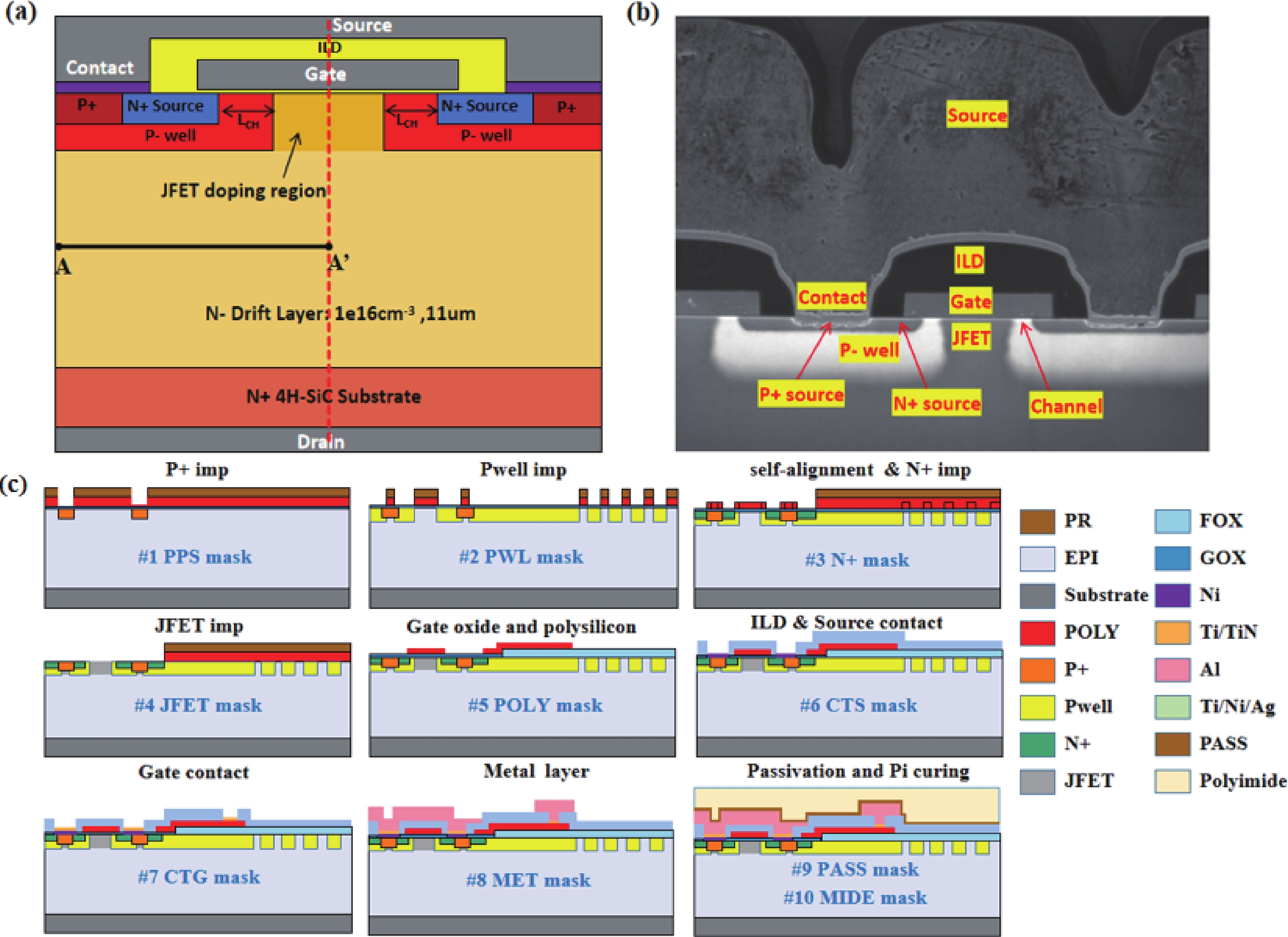
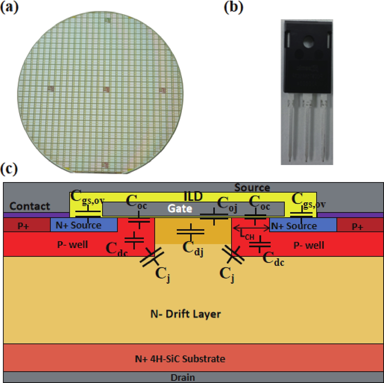
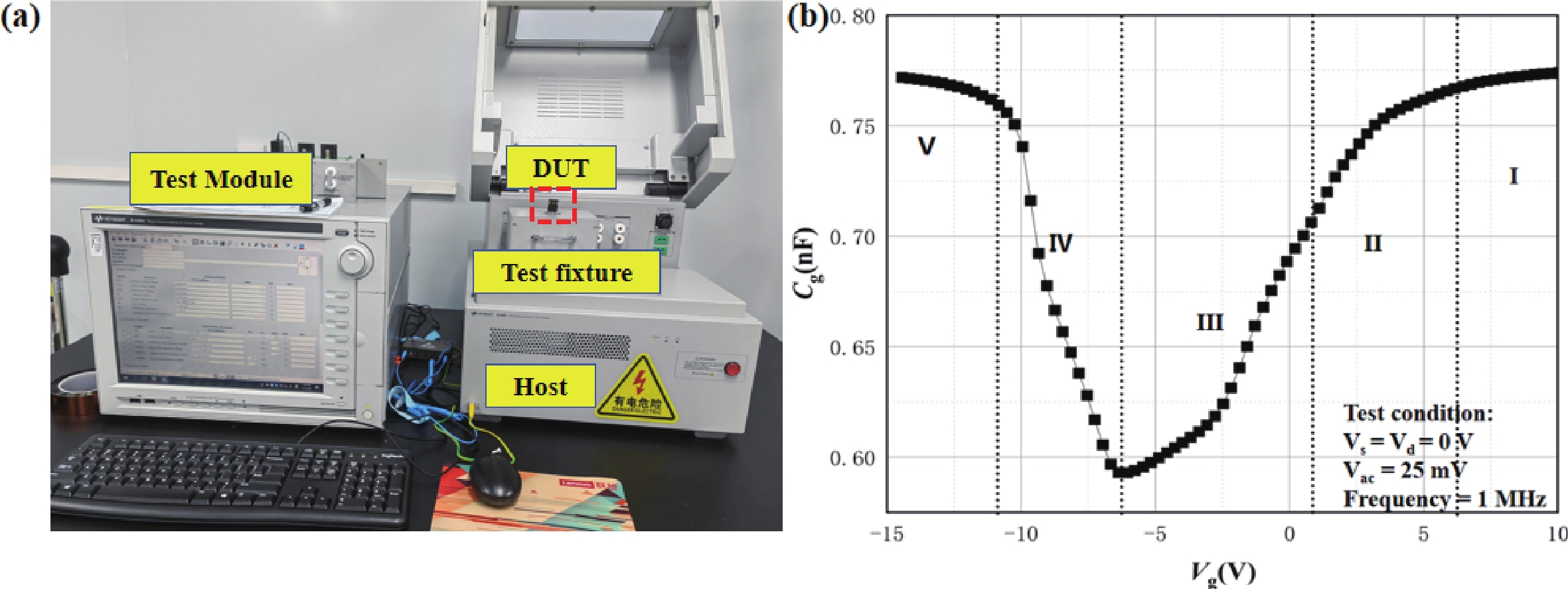
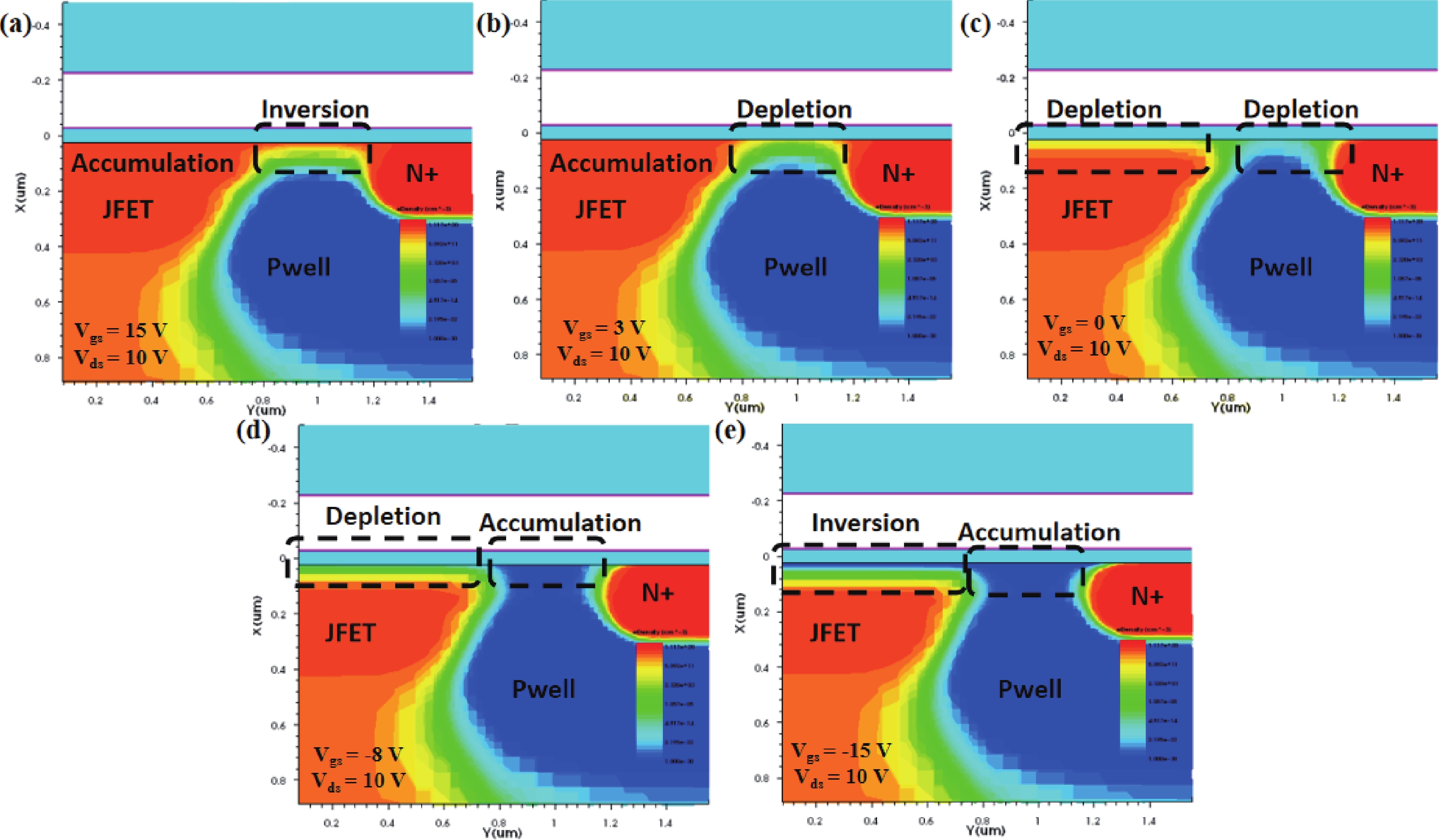
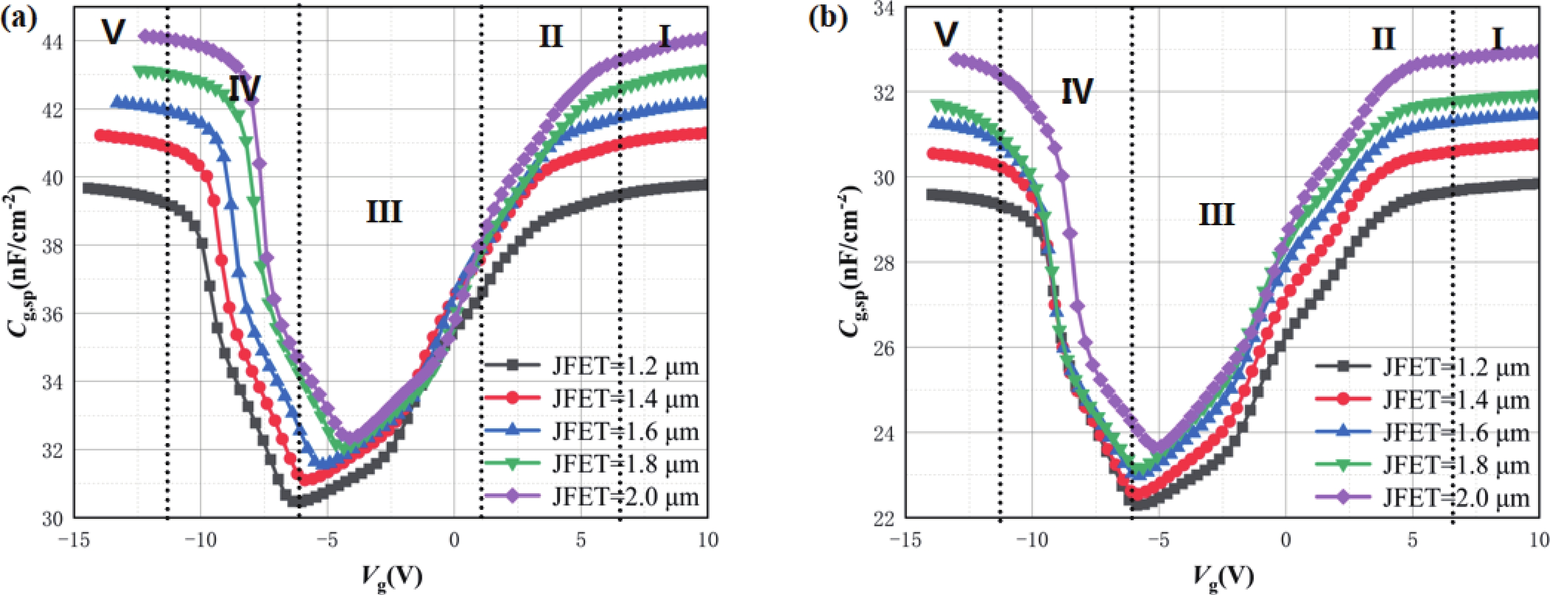
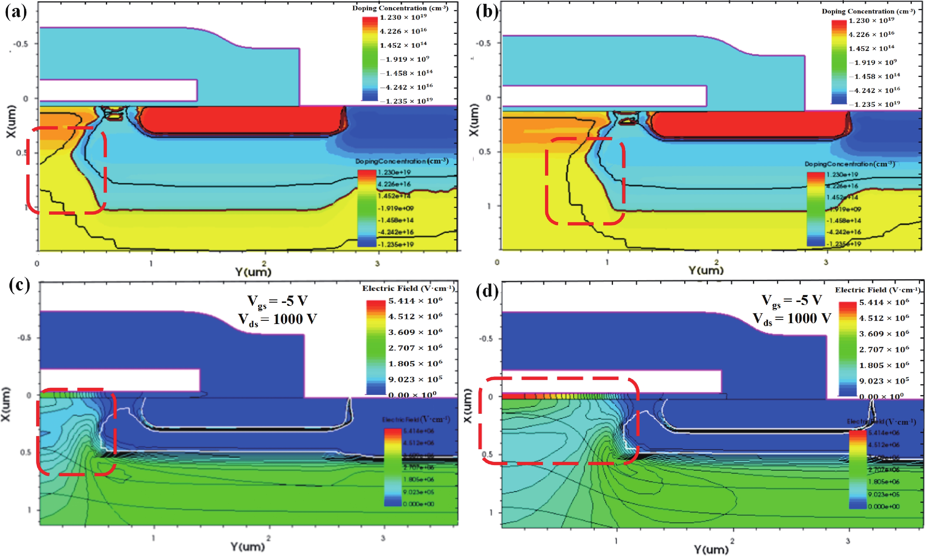
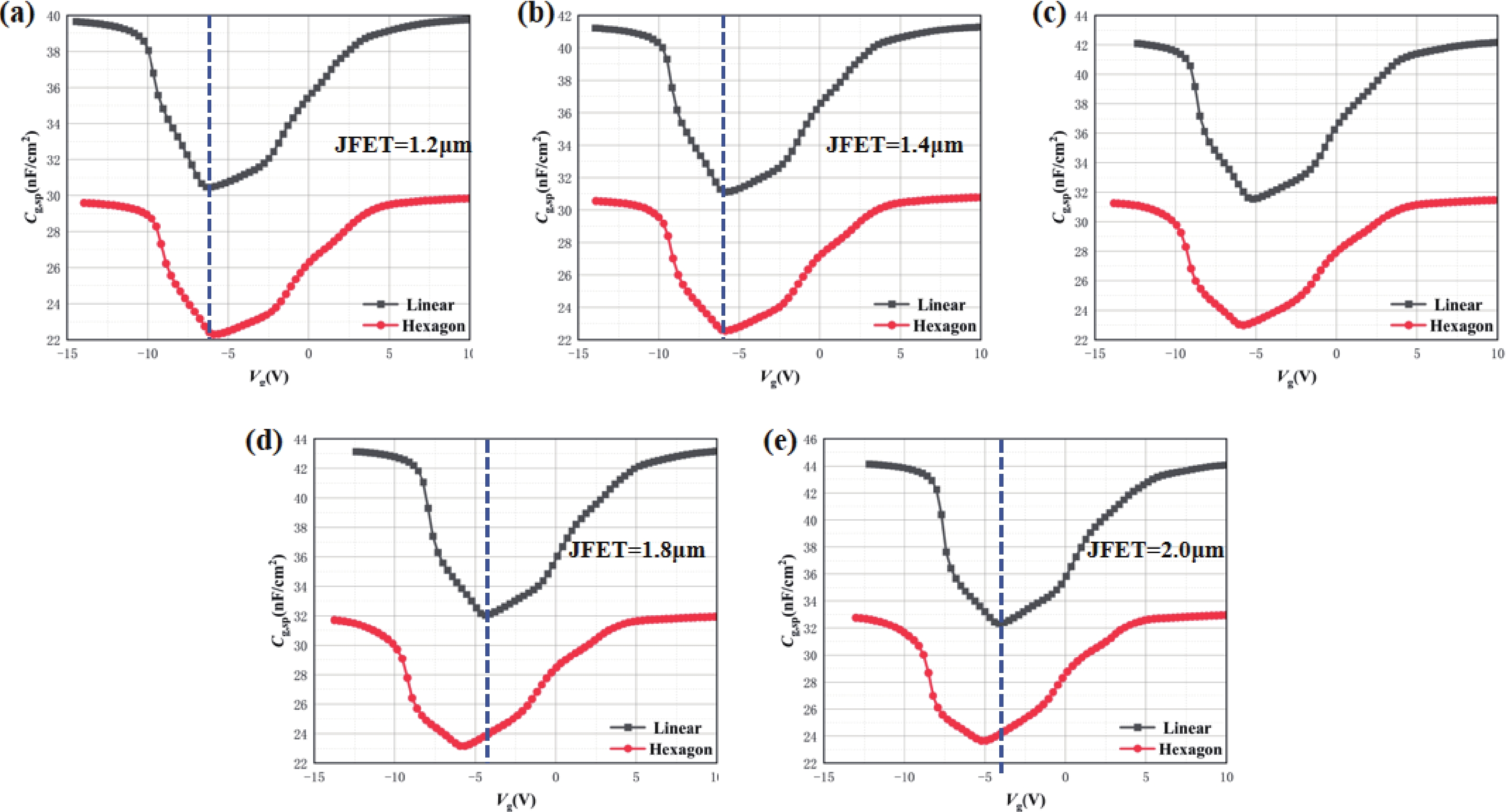
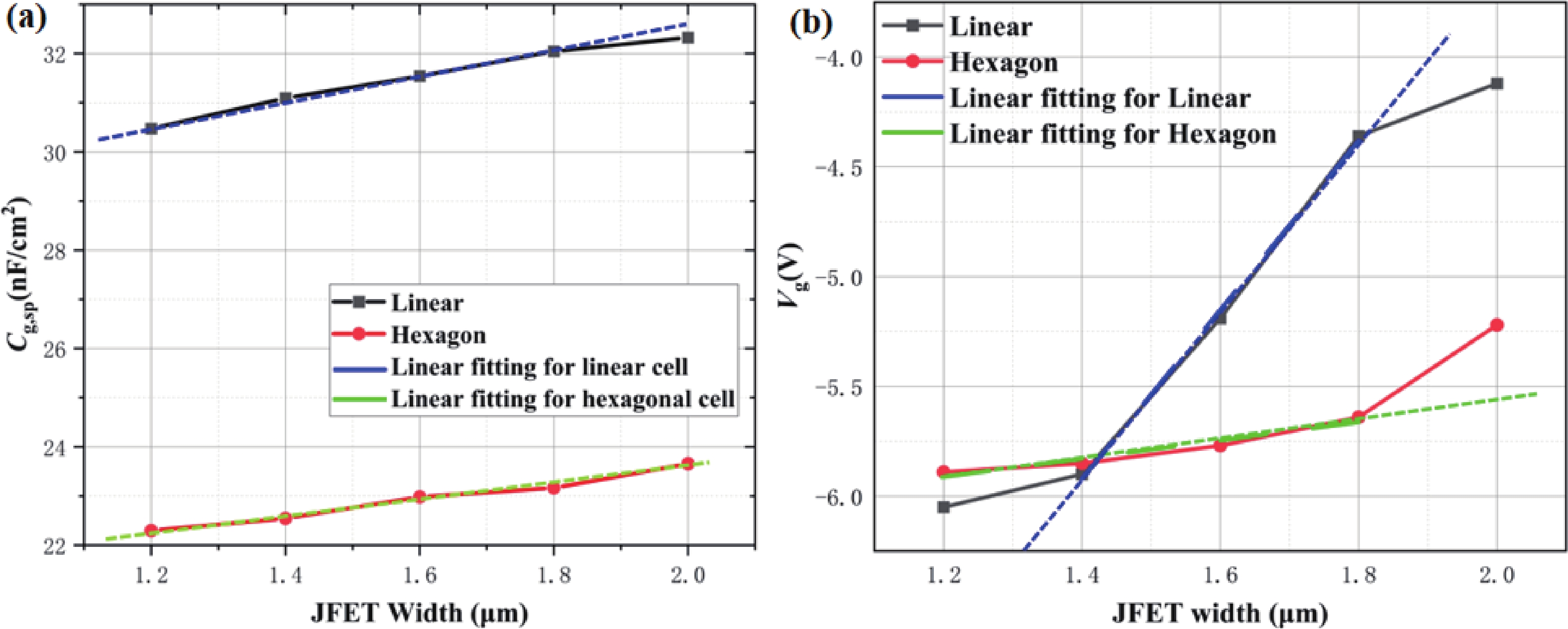
Table 1. 4H-SiC MOSFET structure parameters.
| Symbol | Structure parameter | Value | Unit |
| WP+ | P+ width | 2.0 | μm |
| WN+ | N+ source width | 1.8 | μm |
| LCH | Channel length | 0.5 | μm |
| WJFET | JFET width | 1.2−2.0 | μm |
| Td | Drift thickness | 11 | μm |
| Nd | Drift doping concentration | 1.0 × 10¹⁶ | cm−3 |
| Tox | Gate oxide thickness | 50 | nm |
| Tpoly | Gate poly thickness | 0.5 | μm |
| TILD | Inter level dielectric thickness | 0.95 | μm |
 DownLoad: CSV
Table 2. 4H-SiC MOSFET structure parameters.
| Cell topology | Linear | Hexagonal |
| Pitch (μm) | 8 | 8.7 |
| Sact (cm−2) | 0.0973 | 0.1023 |
| Channel density | 0.125 | 0.174 |
| JFET density | 0.2 | 0.334 |
| BV (V) | 1573 | 1319 |
| Vth (V) | 3.24 | 3.08 |
| Rds,on (mΩ) | 63 | 41 |
| *BV@Vgs = 0 V, Id = 100 μA; *Rds,on@Vgs = 20 V, Id = 20 A; *Vth@Vds = Vgs, Id = 0.4 mV/Rds,on. | ||
DownLoad: CSV
Table 3. Vg−Cg data of SiC MOSFET when it is completely depleted in the JFET region.
| Topology | Linear cell | Hexagonal cell | ||||
| JFET width (μm) | Vg (V) | Cg (nF/cm2) | Vg (V) | Cg (nF/cm2) | ||
| 1.2 | −6.05 | 30.47 | −5.89 | 22.30 | ||
| 1.4 | −5.9 | 31.09 | −5.85 | 22.54 | ||
| 1.6 | −5.19 | 31.54 | −5.77 | 22.98 | ||
| 1.8 | −4.36 | 32.04 | −5.64 | 23.17 | ||
| 2.0 | −4.12 | 32.33 | −5.22 | 23.66 | ||
DownLoad: CSV
Table 4. 4H-SiC MOSFET voltage drift and density of the charge before and after HTGB−.
| Cell topology | JFET width (μm) | ΔVg (V) |
ΔDot (cm−2) |
| Linear cell | 1.2 | −2.56 | 1.1 × 10¹² |
| Linear cell | 1.6 | −3.77 | 1.63 × 10¹² |
| Linear cell | 2.0 | −3.94 | 1.70 × 10¹² |
| Hexagonal cell | 1.2 | −4.04 | 1.74 × 10¹² |
| Hexagonal cell | 1.6 | −4.16 | 1.79 × 10¹² |
| Hexagonal cell | 2.0 | −4.2 | 1.81 × 10¹² |
DownLoad: CSV
| [1] |
Weitzel C E, Palmour J W, Carter C H, et al. Silicon carbide high-power devices. IEEE Trans Electron Devices, 1996, 43(10): 1732 doi: 10.1109/16.536819
|
| [2] |
Callanan R J, Agarwal A, Burk A, et al. Recent progress in SiC DMOSFETs and JBS diodes at cree. 2008 34th Annual Conference of IEEE Industrial Electronics, 2008: 2885 doi: 10.1109/IECON.2008.4758417
|
| [3] |
Rupp R. CoolSiC™ and major trends in SiC power device development. 2017 47th European Solid-State Device Research Conference (ESSDERC), 2017: 118 doi: 10.1109/ESSDERC.2017.8066606
|
| [4] |
Millán J, Godignon P, Perpiñà X, et al. A survey of wide bandgap power semiconductor devices. IEEE Trans Power Electron, 2014, 29(5): 2155 doi: 10.1109/TPEL.2013.2268900
|
| [5] |
Ostling M, Ghandi R, Zetterling C M. SiC power devices—Present status, applications and future perspective. 2011 IEEE 23rd International Symposium on Power Semiconductor Devices and ICs, 2011: 10 doi: 10.1109/ISPSD.2011.5890778
|
| [6] |
A Khan, A Imran, M Hasan. A 2.25kV, 6.1mΩ-cm2 4H-SiC normally-off VJFET. 2012 2nd International Conference on Power, Control and Embedded Systems, 2012: 1 doi: 10.1109/ICPCES.2012.6508119
|
| [7] |
Afanas’ev V V, Stesmans A, Bassler M, et al. Shallow electron traps at the 4H–SiC/SiO2 interface. Appl Phys Lett, 2000, 76(3): 336 doi: 10.1063/1.125737
|
| [8] |
Chung G Y, Tin C C, Williams J R, et al. Improved inversion channel mobility for 4H-SiC MOSFETs following high temperature anneals in nitric oxide. IEEE Electron Device Lett, 2001, 22(4): 176 doi: 10.1109/55.915604
|
| [9] |
Kong M F, Hou Y R, Yi B, et al. A high speed high voltage normally-off SiC vertical JFET power device. 2019 IEEE International Conference on Electron Devices and Solid-State Circuits (EDSSC), 2019: 1 doi: 10.1109/EDSSC.2019.8754097
|
| [10] |
Treu M, Rupp R, Blaschitz P, et al. Strategic considerations for unipolar SiC switch options: JFET vs. MOSFET. 2007 IEEE Industry Applications Annual Meeting, 2007: 324 doi: 10.1109/07IAS.2007.10
|
| [11] |
Zhou W C, Zhong X Q, Sheng K. High temperature stability and the performance degradation of SiC MOSFETs. IEEE Trans Power Electron, 2014, 29(5): 2329 doi: 10.1109/TPEL.2013.2283509
|
| [12] |
Ji S Q, Zheng S, Wang F, et al. Temperature-dependent characterization, modeling, and switching speed-limitation analysis of third-generation 10-kV SiC MOSFET. IEEE Trans Power Electron, 2018, 33(5): 4317 doi: 10.1109/TPEL.2017.2723601
|
| [13] |
Gonzalez J O, Alatise O, Hu J, et al. An investigation of temperature-sensitive electrical parameters for SiC power MOSFETs. IEEE Trans Power Electron, 2017, 32(10): 7954 doi: 10.1109/TPEL.2016.2631447
|
| [14] |
Soler V, Cabello M, Montserrat J, et al. 4.5kV SiC MOSFET with boron doped gate dielectric. 2016 28th International Symposium on Power Semiconductor Devices and ICs (ISPSD), 2016: 283 doi: 10.1109/ISPSD.2016.7520833
|
| [15] |
Noguchi M, Iwamatsu T, Amishiro H, et al. Determination of intrinsic phonon-limited mobility and carrier transport property extraction of 4H-SiC MOSFETs. 2017 IEEE International Electron Devices Meeting (IEDM), 2017: 9.3.1 doi: 10.1109/IEDM.2017.8268358
|
| [16] |
Deboy G, Treu M, Haeberlen O, et al. Si, SiC and GaN power devices: An unbiased view on key performance indicators. 2016 IEEE International Electron Devices Meeting (IEDM), 2016: 20.2.1 doi: 10.1109/IEDM.2016.7838458
|
| [17] |
Wu H, Luo H C, Zhang J P, et al. Investigation of unclamped inductive switch characteristics in 4H-SiC MOSFETs with different cell topologies. IEEE Trans Electron Devices, 2023, 70(3): 1181 doi: 10.1109/TED.2022.3233816
|
| [18] |
Kitai H, Hozumi Y, Shiomi H, et al. Low on-resistance and fast switching of 13-kV SiC MOSFETs with optimized junction field-effect transistor region. 2017 29th International Symposium on Power Semiconductor Devices and IC’s (ISPSD), 2017: 343 doi: 10.23919/ISPSD.2017.7988982
|
| [19] |
Sung W, Han K, Baliga B J. Optimization of the JFET region of 1.2kV SiC MOSFETs for improved high frequency figure of merit (HF-FOM). 2017 IEEE 5th Workshop on Wide Bandgap Power Devices and Applications (WiPDA), 2017: 238 doi: 10.1109/WiPDA.2017.8170553
|
| [20] |
Zhu S N, Liu T S, Fan J C, et al. A new cell topology for 4H-SiC planar power MOSFETs for high-frequency switching. Materials, 2022, 15(19): 6690 doi: 10.3390/ma15196690
|
| [21] |
Losee P A, Bolotnikov A, Yu L C, et al. SiC MOSFET design considerations for reliable high voltage operation. 2017 IEEE International Reliability Physics Symposium (IRPS), 2017: 2A doi: 10.1109/IRPS.2017.7936254
|
| [22] |
Donato N, Naydenov K, Udrea F, et al. On the short circuit electro-thermal failure of 1.2 kV 4H-SiC MOSFETs with 3D cell layouts. Mater Sci Forum, 2022, 1062: 632 doi: 10.4028/p-fnekfr
|
| [23] |
Agarwal A, Han K, Baliga B J. Impact of cell topology on characteristics of 600V 4H-SiC planar MOSFETs. IEEE Electron Device Lett, 2019, 40(5): 773 doi: 10.1109/LED.2019.2908078
|
| [24] |
Naydenov K, Donato N, Udrea F, et al. Clamped and unclamped inductive switching of 3.3 kV 4H-SiC MOSFETs with 3D cellular layouts. Mater Sci Forum, 2022, 1062: 627 doi: 10.4028/p-s1v84y
|
| [25] |
Wu H, Luo H C, Zhang J P, et al. Comparison and analysis on static and dynamic performance of 1.2-kV SiC planar MOSFETs with different cell topologies. Mater Sci Semicond Process, 2024, 184: 108849 doi: 10.1016/j.mssp.2024.108849
|
| [26] |
Wang J, Zhao T F, Li J, et al. Characterization, modeling, and application of 10-kV SiC MOSFET. IEEE Trans Electron Devices, 2008, 55(8): 1798 doi: 10.1109/TED.2008.926650
|
| [27] |
McNutt T R, Hefner A R, Mantooth H A, et al. Silicon carbide power MOSFET model and parameter extraction sequence. IEEE Trans Power Electron, 2007, 22(2): 353 doi: 10.1109/TPEL.2006.889890
|
| [28] |
DeBoer S, Jang S Y, Morgan A, et al. Optimization of jfet region for 1.2kV SiC HEXFETs with 3d tcad simulations. 2024 IEEE 11th Workshop on Wide Bandgap Power Devices & Applications (WiPDA), 2024: 1 doi: 10.1109/WiPDA62103.2024.10773373
|


Article views: 1333 Times PDF downloads: 177 Times Cited by: 0 Times
Received: 26 June 2025 Revised: 06 November 2025 Online: Accepted Manuscript: 15 December 2025Uncorrected proof: 17 December 2025Published: 21 April 2026
| Citation: |
Bofeng Zheng, Houcai Luo, Huan Wu, Jingping Zhang, Xianping Chen. Effects of cell topology and JFET width on depletion layer of SiC MOSFET[J]. Journal of Semiconductors, 2026, 47(4): 042102. doi: 10.1088/1674-4926/25060030
****
B F Zheng, H C Luo, H Wu, J P Zhang, and X P Chen, Effects of cell topology and JFET width on depletion layer of SiC MOSFET[J]. J. Semicond., 2026, 47(4): 042102 doi: 10.1088/1674-4926/25060030

|
 Bofeng Zheng received the M.S. degree in Material Physics from Friedrich-Alexander-Universität Erlangen-Nürnberg, Germany, in 2020. He is currently working toward the D.Eng. degree in Instrument Science and Technology at the College of Optoelectronic Engineering, Chongqing University, Chongqing, China. His research interests include optimization design, robustness, and reliability research of third-generation power semiconductor devices (SiC and GaN)
 Houcai Luo received the B.S. and M.S. degree from the School of Mechanical and Electrical Engineering, Guilin University of Electronic Technology, Guilin, China, in 2016, and 2019, respectively. He is currently working toward the Ph.D. degree at the College of Optoelectronic Engineering, Chongqing University, Chongqing, China. His research interests include the development of silicon carbide power electronics and analysis of their reliability
 Huan Wu received the B.S. degree in Measurement and Control Technology and Instrument from Chongqing University, Chongqing, China, in 2020. He is currently working toward the Ph.D. degree in Instrument Science and Technology at the College of Optoelectronic Engineering, Chongqing University, Chongqing, China. His research interests include optimization design, robustness, and reliability research of wide bandgap power semiconductor devices
 Jingping Zhang received the B.S. degree in Electronic Science and Technology from Chongqing University, Chongqing, China, in 2020. He is currently working toward the Ph.D. degree in Instrument Science and Technology at the College of Optoelectronic Engineering, Chongqing University, Chongqing, China. His research interests include optimization design, robustness, and reliability research of power semiconductor devices
 Xianping Chen (Senior Member, IEEE) received the B.Eng. degree in electrical engineering from Chongqing University, Chongqing, China, in 2002, the M.Sc. degree in bioelectronics from Dresden University of Technology, Dresden, Germany, in 2006, and the Ph.D. degree in semiconductor from Delft University of Technology, Delft, The Netherlands, in 2013. He is currently a Distinguished Professor of Microelectronics and Microsystems with the College of Optoelectronic Engineering, Chongqing University. His research interests include advanced sensor and intelligent sensing technology; power semiconductor device design, packaging, and reliability; and new electronic materials and devices
| [1] |
Weitzel C E, Palmour J W, Carter C H, et al. Silicon carbide high-power devices. IEEE Trans Electron Devices, 1996, 43(10): 1732 doi: 10.1109/16.536819
|
| [2] |
Callanan R J, Agarwal A, Burk A, et al. Recent progress in SiC DMOSFETs and JBS diodes at cree. 2008 34th Annual Conference of IEEE Industrial Electronics, 2008: 2885 doi: 10.1109/IECON.2008.4758417
|
| [3] |
Rupp R. CoolSiC™ and major trends in SiC power device development. 2017 47th European Solid-State Device Research Conference (ESSDERC), 2017: 118 doi: 10.1109/ESSDERC.2017.8066606
|
| [4] |
Millán J, Godignon P, Perpiñà X, et al. A survey of wide bandgap power semiconductor devices. IEEE Trans Power Electron, 2014, 29(5): 2155 doi: 10.1109/TPEL.2013.2268900
|
| [5] |
Ostling M, Ghandi R, Zetterling C M. SiC power devices—Present status, applications and future perspective. 2011 IEEE 23rd International Symposium on Power Semiconductor Devices and ICs, 2011: 10 doi: 10.1109/ISPSD.2011.5890778
|
| [6] |
A Khan, A Imran, M Hasan. A 2.25kV, 6.1mΩ-cm2 4H-SiC normally-off VJFET. 2012 2nd International Conference on Power, Control and Embedded Systems, 2012: 1 doi: 10.1109/ICPCES.2012.6508119
|
| [7] |
Afanas’ev V V, Stesmans A, Bassler M, et al. Shallow electron traps at the 4H–SiC/SiO2 interface. Appl Phys Lett, 2000, 76(3): 336 doi: 10.1063/1.125737
|
| [8] |
Chung G Y, Tin C C, Williams J R, et al. Improved inversion channel mobility for 4H-SiC MOSFETs following high temperature anneals in nitric oxide. IEEE Electron Device Lett, 2001, 22(4): 176 doi: 10.1109/55.915604
|
| [9] |
Kong M F, Hou Y R, Yi B, et al. A high speed high voltage normally-off SiC vertical JFET power device. 2019 IEEE International Conference on Electron Devices and Solid-State Circuits (EDSSC), 2019: 1 doi: 10.1109/EDSSC.2019.8754097
|
| [10] |
Treu M, Rupp R, Blaschitz P, et al. Strategic considerations for unipolar SiC switch options: JFET vs. MOSFET. 2007 IEEE Industry Applications Annual Meeting, 2007: 324 doi: 10.1109/07IAS.2007.10
|
| [11] |
Zhou W C, Zhong X Q, Sheng K. High temperature stability and the performance degradation of SiC MOSFETs. IEEE Trans Power Electron, 2014, 29(5): 2329 doi: 10.1109/TPEL.2013.2283509
|
| [12] |
Ji S Q, Zheng S, Wang F, et al. Temperature-dependent characterization, modeling, and switching speed-limitation analysis of third-generation 10-kV SiC MOSFET. IEEE Trans Power Electron, 2018, 33(5): 4317 doi: 10.1109/TPEL.2017.2723601
|
| [13] |
Gonzalez J O, Alatise O, Hu J, et al. An investigation of temperature-sensitive electrical parameters for SiC power MOSFETs. IEEE Trans Power Electron, 2017, 32(10): 7954 doi: 10.1109/TPEL.2016.2631447
|
| [14] |
Soler V, Cabello M, Montserrat J, et al. 4.5kV SiC MOSFET with boron doped gate dielectric. 2016 28th International Symposium on Power Semiconductor Devices and ICs (ISPSD), 2016: 283 doi: 10.1109/ISPSD.2016.7520833
|
| [15] |
Noguchi M, Iwamatsu T, Amishiro H, et al. Determination of intrinsic phonon-limited mobility and carrier transport property extraction of 4H-SiC MOSFETs. 2017 IEEE International Electron Devices Meeting (IEDM), 2017: 9.3.1 doi: 10.1109/IEDM.2017.8268358
|
| [16] |
Deboy G, Treu M, Haeberlen O, et al. Si, SiC and GaN power devices: An unbiased view on key performance indicators. 2016 IEEE International Electron Devices Meeting (IEDM), 2016: 20.2.1 doi: 10.1109/IEDM.2016.7838458
|
| [17] |
Wu H, Luo H C, Zhang J P, et al. Investigation of unclamped inductive switch characteristics in 4H-SiC MOSFETs with different cell topologies. IEEE Trans Electron Devices, 2023, 70(3): 1181 doi: 10.1109/TED.2022.3233816
|
| [18] |
Kitai H, Hozumi Y, Shiomi H, et al. Low on-resistance and fast switching of 13-kV SiC MOSFETs with optimized junction field-effect transistor region. 2017 29th International Symposium on Power Semiconductor Devices and IC’s (ISPSD), 2017: 343 doi: 10.23919/ISPSD.2017.7988982
|
| [19] |
Sung W, Han K, Baliga B J. Optimization of the JFET region of 1.2kV SiC MOSFETs for improved high frequency figure of merit (HF-FOM). 2017 IEEE 5th Workshop on Wide Bandgap Power Devices and Applications (WiPDA), 2017: 238 doi: 10.1109/WiPDA.2017.8170553
|
| [20] |
Zhu S N, Liu T S, Fan J C, et al. A new cell topology for 4H-SiC planar power MOSFETs for high-frequency switching. Materials, 2022, 15(19): 6690 doi: 10.3390/ma15196690
|
| [21] |
Losee P A, Bolotnikov A, Yu L C, et al. SiC MOSFET design considerations for reliable high voltage operation. 2017 IEEE International Reliability Physics Symposium (IRPS), 2017: 2A doi: 10.1109/IRPS.2017.7936254
|
| [22] |
Donato N, Naydenov K, Udrea F, et al. On the short circuit electro-thermal failure of 1.2 kV 4H-SiC MOSFETs with 3D cell layouts. Mater Sci Forum, 2022, 1062: 632 doi: 10.4028/p-fnekfr
|
| [23] |
Agarwal A, Han K, Baliga B J. Impact of cell topology on characteristics of 600V 4H-SiC planar MOSFETs. IEEE Electron Device Lett, 2019, 40(5): 773 doi: 10.1109/LED.2019.2908078
|
| [24] |
Naydenov K, Donato N, Udrea F, et al. Clamped and unclamped inductive switching of 3.3 kV 4H-SiC MOSFETs with 3D cellular layouts. Mater Sci Forum, 2022, 1062: 627 doi: 10.4028/p-s1v84y
|
| [25] |
Wu H, Luo H C, Zhang J P, et al. Comparison and analysis on static and dynamic performance of 1.2-kV SiC planar MOSFETs with different cell topologies. Mater Sci Semicond Process, 2024, 184: 108849 doi: 10.1016/j.mssp.2024.108849
|
| [26] |
Wang J, Zhao T F, Li J, et al. Characterization, modeling, and application of 10-kV SiC MOSFET. IEEE Trans Electron Devices, 2008, 55(8): 1798 doi: 10.1109/TED.2008.926650
|
| [27] |
McNutt T R, Hefner A R, Mantooth H A, et al. Silicon carbide power MOSFET model and parameter extraction sequence. IEEE Trans Power Electron, 2007, 22(2): 353 doi: 10.1109/TPEL.2006.889890
|
| [28] |
DeBoer S, Jang S Y, Morgan A, et al. Optimization of jfet region for 1.2kV SiC HEXFETs with 3d tcad simulations. 2024 IEEE 11th Workshop on Wide Bandgap Power Devices & Applications (WiPDA), 2024: 1 doi: 10.1109/WiPDA62103.2024.10773373
|

 WeChat ID
Journal of Semiconductors © 2017 All Rights Reserved 京ICP备05085259号-2


