| Citation: |
Kyung Min Kim, Sang Han Ko, Sung Min Yoon. Strategical dynamic modulation of turn-on voltage for write transistor introducing charge-trap layer in 2T0C DRAM cell employing IGZO channel[J]. Journal of Semiconductors, 2026, 47(2): 022301. doi: 10.1088/1674-4926/25050019
****
K M Kim, S H Ko, and S M Yoon, Strategical dynamic modulation of turn-on voltage for write transistor introducing charge-trap layer in 2T0C DRAM cell employing IGZO channel[J]. J. Semicond., 2026, 47(2): 022301 doi: 10.1088/1674-4926/25050019
|
Strategical dynamic modulation of turn-on voltage for write transistor introducing charge-trap layer in 2T0C DRAM cell employing IGZO channel
DOI: 10.1088/1674-4926/25050019
CSTR: 32376.14.1674-4926.25050019
More Information-
Abstract
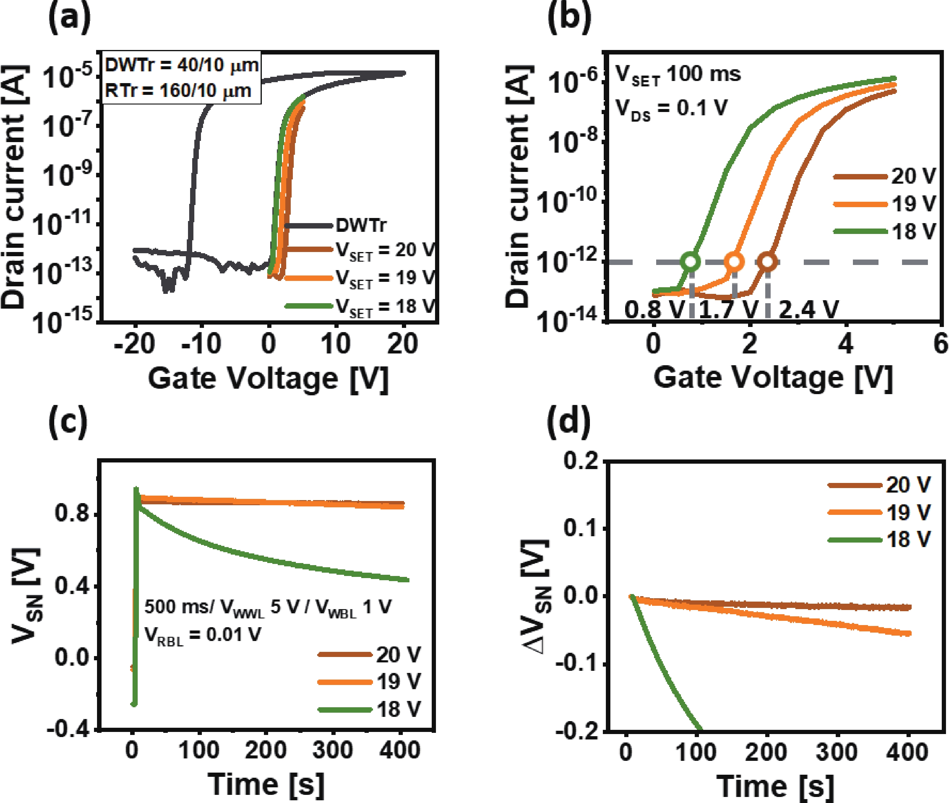
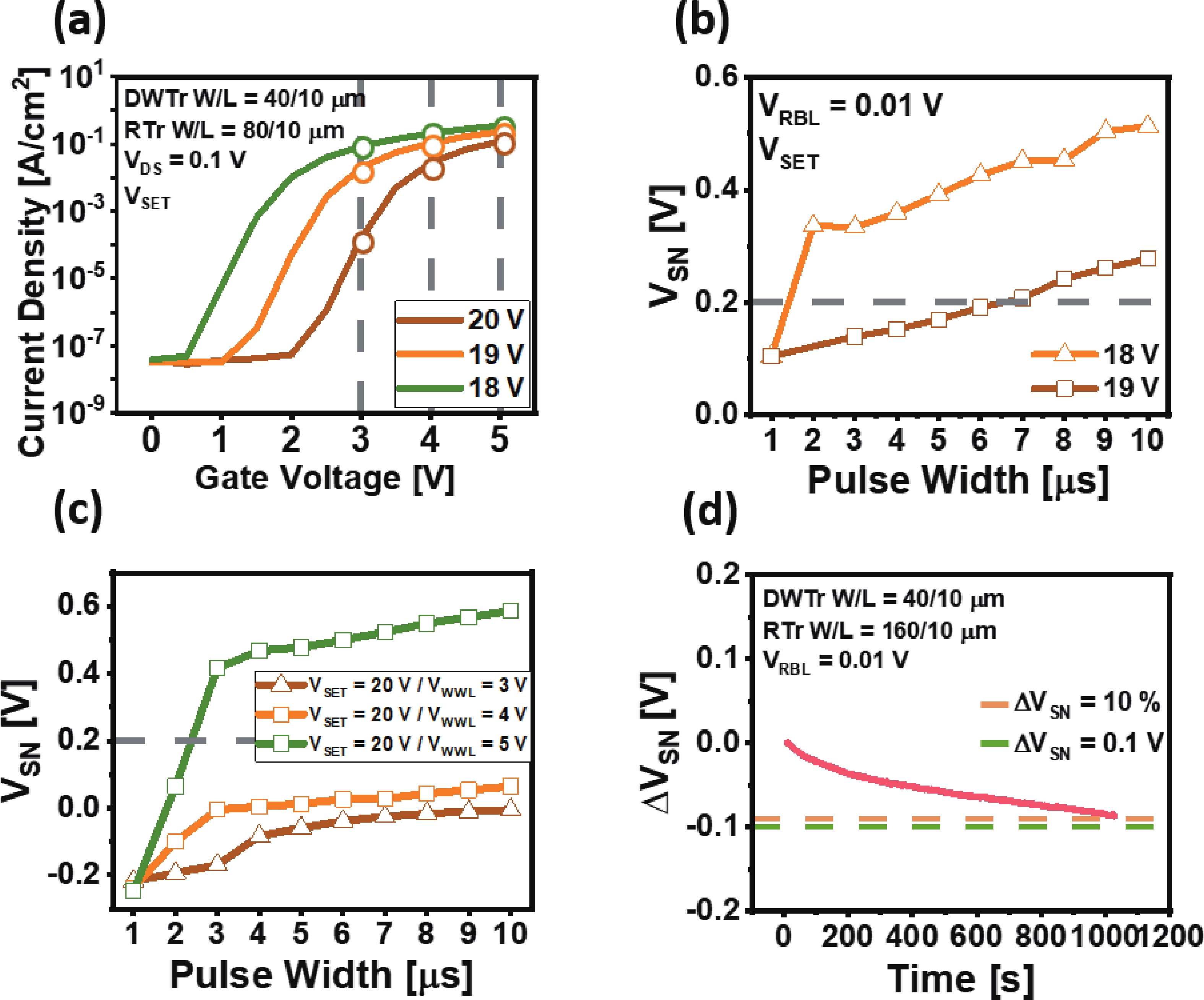
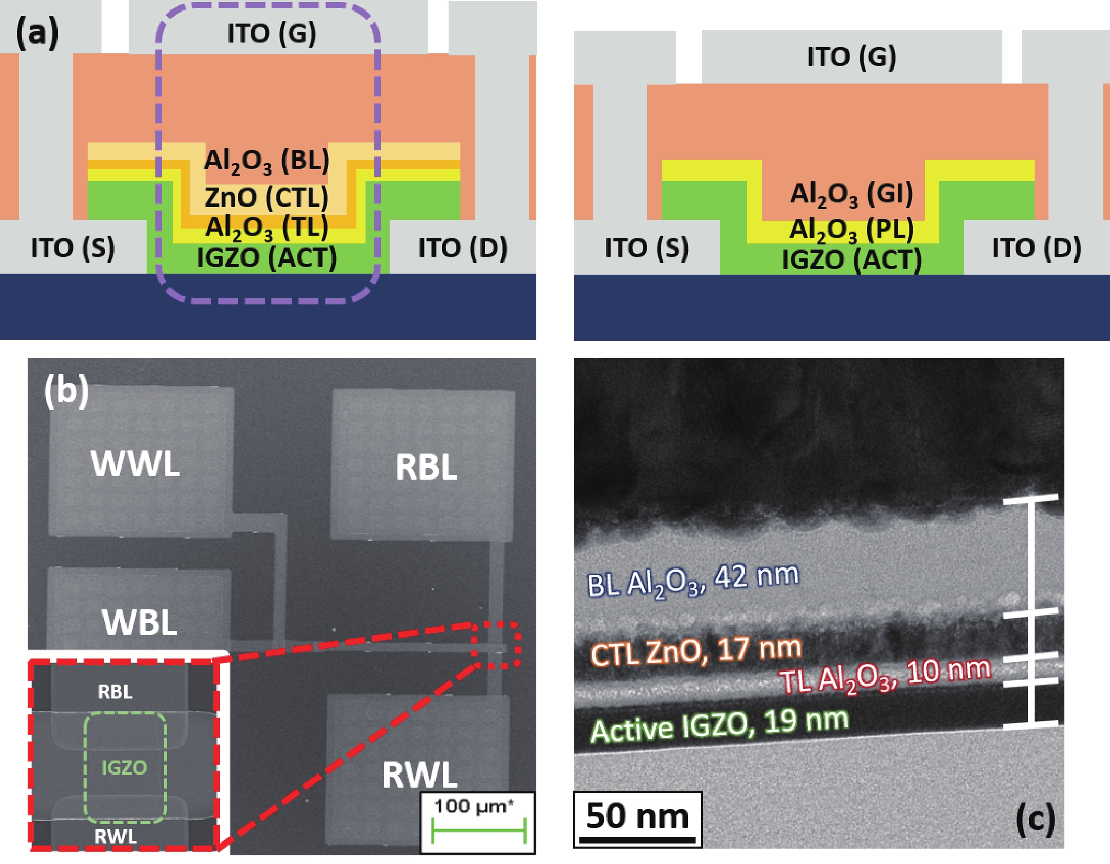
The fabrication of a dynamic threshold-2T0C (DT-2T0C) DRAM cell incorporating a ZnO charge-trap layer in the write transistor has been successfully achieved, addressing the negative hold voltage (VHOLD) issue of conventional 2T0C DRAM cells using oxide channel layers. The proposed device facilitates dynamic modulation of turn-on voltage (VON) through an additional SET operation, allowing VON to shift above 0 V. The retention time in SET operation was extended to 104 s by optimizing the tunneling layer deposition conditions. The device characterization revealed a significant correlation between VON and both the WRITE speed and the retention properties of the DT-2T0C, verifying the trade-off between WRITE time and retention time. A long retention time over 1000 s was achieved, even under VHOLD of 0 V. -
References
[1] Kim S E, Sung J Y, Jeon J D, et al. Toward advanced high—k and electrode thin films for DRAM capacitors via atomic layer deposition. Adv Mater Technol, 2023, 8(20): 2200878 doi: 10.1002/admt.202200878[2] Keitel-Schulz D, Wehn N. Embedded DRAM development: Technology, physical design, and application issues. IEEE Des Test Comput, 2001, 18(3): 7 doi: 10.1109/54.922799[3] Nomura K, Ohta H, Takagi A, et al. Room-temperature fabrication of transparent flexible thin-film transistors using amorphous oxide semiconductors. Nature, 2004, 432(7016): 488 doi: 10.1038/nature03090[4] Yabuta H, Sano M, Abe K, et al. High-mobility thin-film transistor with amorphous InGaZnO4 channel fabricated by room temperature rf-magnetron sputtering. Appl Phys Lett, 2006, 89(11): 112123 doi: 10.1063/1.2353811[5] Belmonte A, Oh H, Rassoul N, et al. Capacitor-less, long-retention (>400s) DRAM cell paving the way towards low-power and high-density monolithic 3D DRAM. 2020 IEEE International Electron Devices Meeting (IEDM), 2020: 28.2. 1 doi: 10.1109/IEDM13553.2020.9371900[6] Kamiya T, Nomura K, Hosono H. Electronic Structures above mobility edges in crystalline and amorphous In-Ga-Zn-O: Percolation conduction examined by analytical model. J Disp Technol, 2009, 5(12): 462 doi: 10.1109/JDT.2009.2022064[7] Kamiya T, Nomura K, Hosono H. Present status of amorphous In–Ga–Zn–O thin-film transistors. Sci Technol Adv Mater, 2010, 11(4): 044305 doi: 10.1088/1468-6996/11/4/044305[8] Xiong W, Luo B B, Meng W, et al. Atomic-layer-deposited ultrathin InAlZnO FETs-based 2T0C DRAM cells with long data retention and multilevel storage. IEEE Trans Electron Devices, 2024, 71(4): 2393 doi: 10.1109/TED.2024.3365457[9] Yan G P, Luo Y N, Wang J J, et al. First demonstration of true 4-bit memory with record high multibit retention >103s and read window >105 by hydrogen self-adaptive-doping for IGZO DRAM arrays. 2023 International Electron Devices Meeting (IEDM), 2023: 1 doi: 10.1109/IEDM45741.2023.10413762[10] Lopes M E, Gomes H L, Medeiros M C R, et al. Gate-bias stress in amorphous oxide semiconductors thin-film transistors. Appl Phys Lett, 2009, 95(6): 063502 doi: 10.1063/1.3187532[11] Fung T C, Abe K, Kumomi H, et al. Electrical instability of RF sputter amorphous In-Ga-Zn-O thin-film transistors. J Disp Technol, 2009, 5(12): 452 doi: 10.1109/JDT.2009.2020611[12] Hong T, Kim Y S, Choi S H, et al. Exploration of chemical composition of In–Ga–Zn–O system via PEALD technique for optimal physical and electrical properties. Adv Elect Materials, 2023, 9(4): 2201208 doi: 10.1002/aelm.202201208[13] Yan G P, Yang Y Y, Tai L, et al. Linear tuning of positive threshold voltage in IGZO thin-film transistors via gate dielectric stack engineering. IEEE Electron Device Lett, 2025, 46(5): 781 doi: 10.1109/LED.2025.3553826[14] Ide K, Kikuchi Y, Nomura K, et al. Effects of excess oxygen on operation characteristics of amorphous In-Ga-Zn-O thin-film transistors. Appl Phys Lett, 2011, 99(9): 093507 doi: 10.1063/1.3633100[15] Zhang J, Zhang Z, Dou H, et al. Fluorine anion-doped ultra-thin InGaO transistors overcoming mobility-stability trade-off. 2023 International Electron Devices Meeting (IEDM), 2023: 1 doi: 10.1109/IEDM45741.2023.10413810[16] Hu Q L, Gu C R, Zhu S W, et al. Capacitorless DRAM cells based on high-performance indium-tin-oxide transistors with record data retention and reduced write latency. IEEE Electron Device Lett, 2023, 44(1): 60 doi: 10.1109/LED.2022.3225263[17] Duan X L, Huang K L, Feng J X, et al. Novel vertical channel-all-around (CAA) In-Ga-Zn-O FET for 2T0C-DRAM with high density beyond 4F2 by monolithic stacking. IEEE Trans Electron Devices, 2022, 69(4): 2196 doi: 10.1109/TED.2022.3154693[18] Noh T H, Chen S M, Kim H B, et al. First demonstration of 2T0C-FeDRAM: A-ITZO FET and double gate a-ITZO/a-IGZO FeFET with a record-long multibit retention time of >4-bit and >2000 s. Nanoscale, 2024, 16(35): 16467 doi: 10.1039/D4NR02393E[19] Liu D D, Pei J X, Li L K, et al. Multilevel memory and synaptic characteristics of a-IGZO thin-film transistor with atomic layer–deposited Al2O3/ZnO/Al2O3 stack layers. J Mater Res, 2020, 35(7): 732 doi: 10.1557/jmr.2019.355[20] Bak J Y, Ryu M K, Park S H K, et al. Impact of charge-trap layer conductivity control on device performances of top-gate memory thin-film transistors using IGZO channel and ZnO charge-trap layer. IEEE Trans Electron Devices, 2014, 61(7): 2404 doi: 10.1109/TED.2014.2318751[21] Cho Y J, Kwon Y H, Seong N J, et al. Device feasibility of 60-nm-scaled vertical-channel memory transistors using InGaZnO channel and ZnO charge-trap layers. IEEE Trans Electron Devices, 2024, 71(3): 1839 doi: 10.1109/TED.2024.3350562[22] Bak J Y, Kim S J, Byun C W, et al. Effects of thickness and geometric variations in the oxide gate stack on the nonvolatile memory behaviors of charge-trap memory thin-film transistors. Solid State Electron, 2015, 111: 153 doi: 10.1016/j.sse.2015.06.003[23] Moon S H, Kwon Y H, Seong N J, et al. Performance enhancement of self-aligned coplanar TFTs with ALD-IGZO channels via effective doping from interlayer dielectric. IEEE Electron Device Lett, 2023, 44(7): 1128 doi: 10.1109/LED.2023.3274811[24] Zheng L K, Wang Z H, Lin Z Y, et al. The impact of parasitic capacitance on the memory characteristics of 2T0C DRAM and new writing strategy. IEEE Electron Device Lett, 2023, 44(8): 1284 doi: 10.1109/LED.2023.3287942[25] Cho Y J, Kwon Y H, Seong N J, et al. Impact of channel thickness on device scaling in vertical InGaZnO channel charge-trap memory transistors with ALD Al2O3 tunneling layer. Mater Sci Semicond Process, 2024, 178: 108476 doi: 10.1016/j.mssp.2024.108476[26] Guo J M, Lin Z Y, Che X L, et al. Capacitorless dynamic random access memory with 2D transistors by one-step transfer of van der waals dielectrics and electrodes. ACS Nano, 2025, 19(2): 2848 doi: 10.1021/acsnano.4c15750[27] Xiao K, Wan J, Xie H, et al. High performance Si-MoS2 heterogeneous embedded DRAM. Nature Communications, 2024, 15(1): 9782 doi: 10.1038/s41467-024-54218-w[28] Park J M, Lee S, Lee J, et al. ITZO-based self-aligned top gate thin-film transistor with minimum parasitic capacitance for long-retention 2T0C DRAM. ACS Omega, 2024, 10(1): 1006 doi: 10.1021/acsomega.4c08274 -
Supplements
 Supporting Information.pdf

-
Proportional views


 Kyung Min Kim is currently pursuing a B.S. degree from the Department of Materials Science and Engineering, Kyung Hee University, Yongin, Korea. His research interests include In-Ga-Zn-O (IGZO), thin-film transistor (TFT) and memory device.
 Sang Han Ko received his M.S. degree from Department of Materials Science and Engineering, Kyung Hee University, Yongin, Korea, in 2025.
 Sung Min Yoon received his B.S. degree from the Department of Inorganic Material Engineering, Seoul National University, Korea, in 1995, and his M.S. and Ph.D. degrees from the Department of Applied Electronics, Tokyo Institute of Technology, Japan, in 1997 and 2000, respectively. He was a senior research engineer with ETRI, Korea, from 2001 to 2011. He is currently a Professor with the Department of Materials Science and Engineering, Kyung Hee University, Yongin, Korea. His research interests include electronic materials and semiconductor devices. He is also currently working as an overseas editor for JJAP/APEX.
 DownLoad:
