


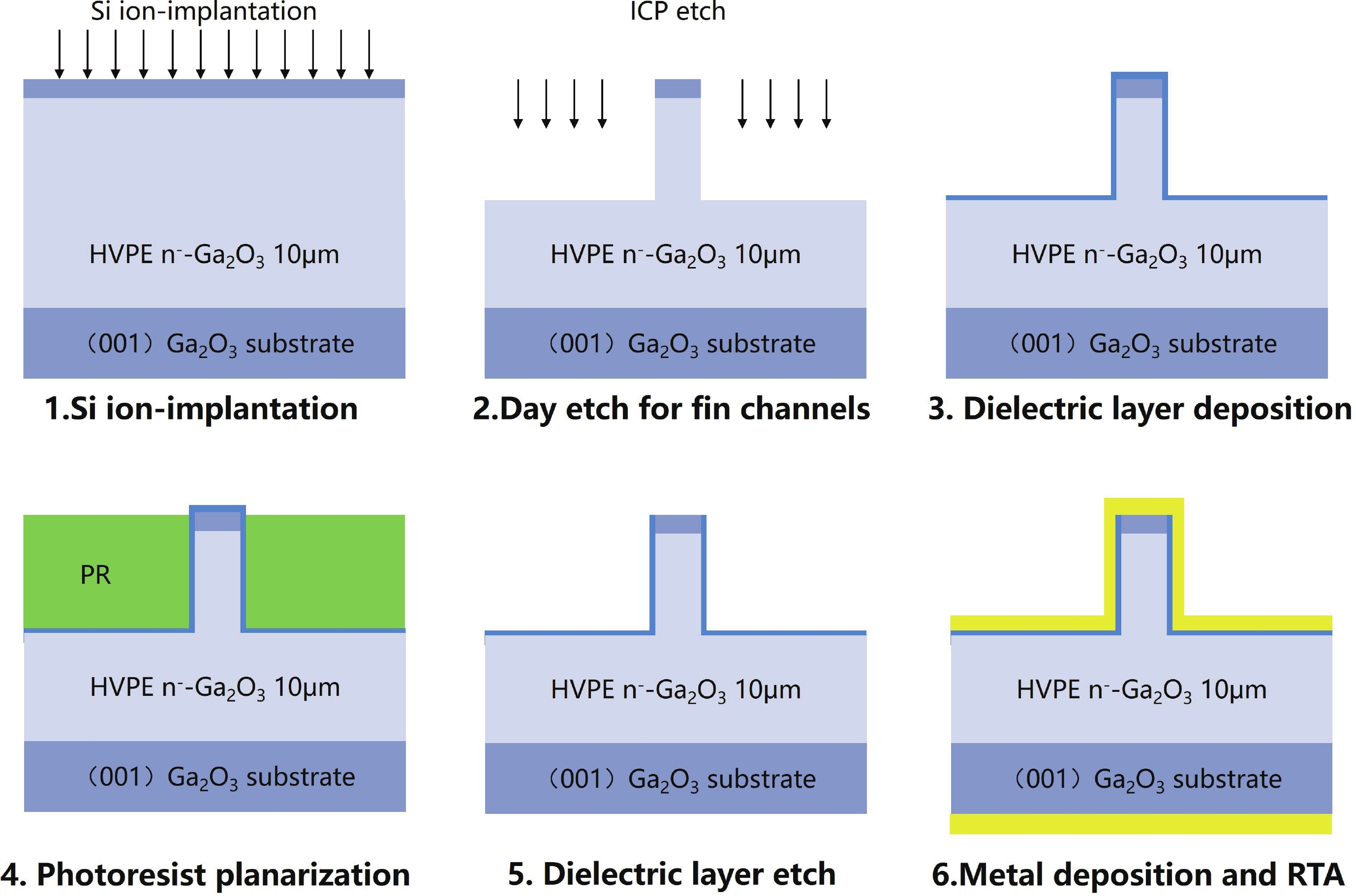
Fig. 1.
(Color online) Complete process flow of the vertical β-Ga2O3 Fin-channel diode fabrication.
ARTICLES
Gaofu Guo1, 2, Xiaodong Zhang2, Chunhong Zeng2, Dong Wei1, Dengrui Zhao1, 2, Tiwei Chen2, Zhucheng Li2, Anjing Luo2, Guangyuan Yu2, 3, Yu Hu2, Zhongming Zeng2, Baoshun Zhang2, and Xianqi Dai1,
Corresponding author: Baoshun Zhang, bszhang2006@sinano.ac.cn; Xianqi Dai, xqdai@htu.edu.cn
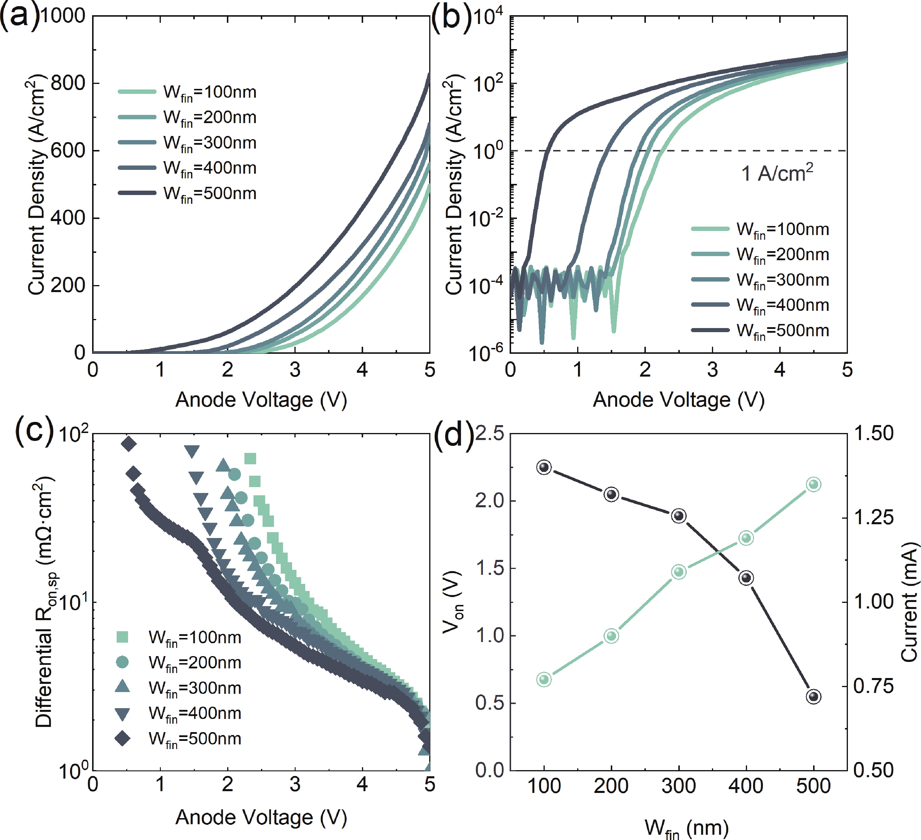
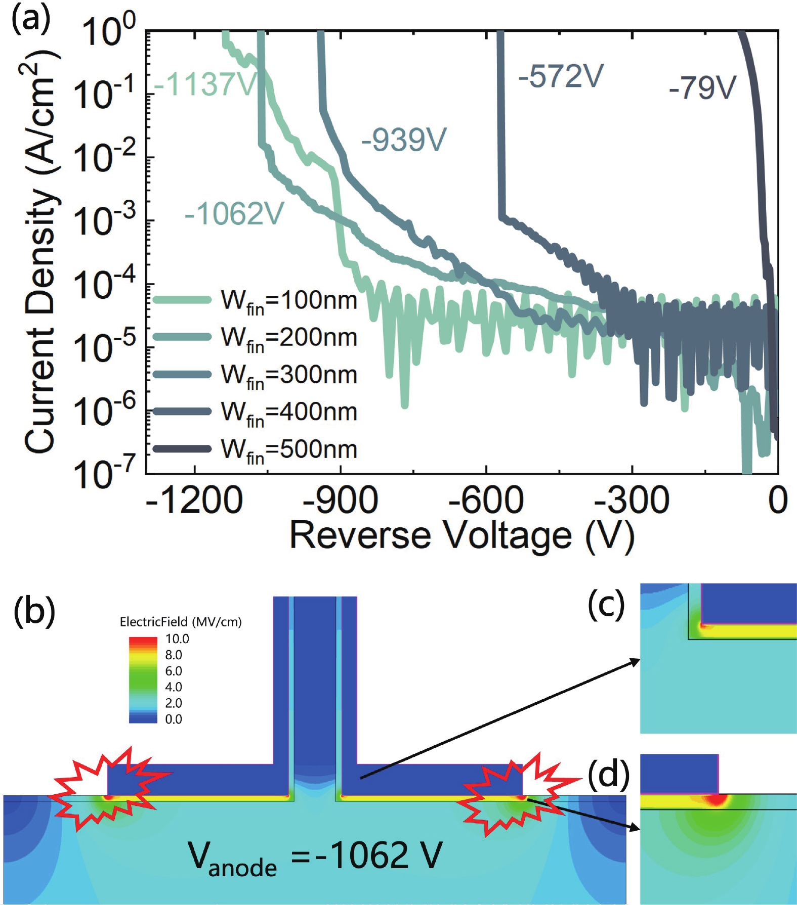
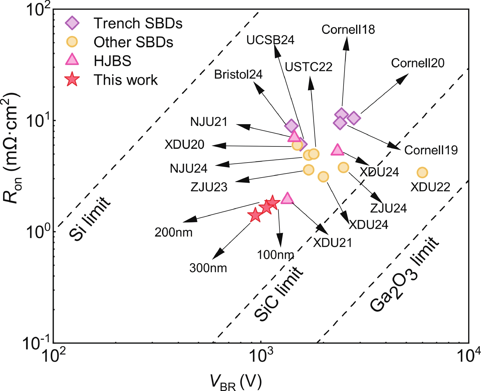
Abstract: This study presents a β-Ga2O3 diode featuring a Fin-channel structure and an anode ohmic contact. The device turn-off is facilitated by the depletion effect induced by the work function difference between the sidewall metal and β-Ga2O3. As the forward bias increases, electron accumulation occurs on the Fin-channel sidewalls, reducing the on-resistance and improving the forward characteristics. Moreover, the device exhibits the reduced surface field (RESURF) effect, similar to trench schottky barrier diodes (SBDs), which shifts the electric field at the fin corners and enhances the breakdown voltage. For a device with a 100 nm fin width (Wfin), we achieved a breakdown voltage (BV) of 1137 V, a specific on-resistance (Ron,sp) of 1.8 mΩ·cm2, and a power figure of merit (PFOM) of 0.72 GW/cm2. This work expands the fabrication approach for β-Ga2O3-based devices, advancing their potential for high-performance applications.
Keywords: β-Ga2O3, Fin-channel diode, self-align, RESUFE, breakdown voltage
| [1] |
Waseem A, Ren Z J, Huang H C, et al. A review of recent progress in β-Ga2O3 epitaxial growth: Effect of substrate orientation and precursors in metal−organic chemical vapor deposition. Phys Status Solidi A, 2023, 220(8): 2200616 doi: 10.1002/pssa.202200616
|
| [2] |
Pearton S J, Yang J C, Cary P H IV, et al. A review of Ga2O3 materials, processing, and devices. Appl Phys Rev, 2018, 5: 011301 doi: 10.1063/1.5006941
|
| [3] |
Spencer J A, Mock A L, Jacobs A G, et al. A review of band structure and material properties of transparent conducting and semiconducting oxides: Ga2O3, Al2O3, In2O3, ZnO, SnO2, CdO, NiO, CuO, and Sc2O3. Appl Phys Rev, 2022, 9: 011315 doi: 10.1063/5.0078037
|
| [4] |
Peterson C, Bhattacharyya A, Chanchaiworawit K, et al. 200 cm2/(V∙s) electron mobility and controlled low 1015 cm−3 Si doping in (010) β-Ga2O3 epitaxial drift layers. Appl Phys Lett, 2024, 125(18): 182103 doi: 10.1063/5.0230413
|
| [5] |
Higashiwaki M, Wong M H. Beta-gallium oxide material and device technologies. Annu Rev Mater Res, 2024, 54: 175 doi: 10.1146/annurev-matsci-080921-104058
|
| [6] |
Zheng X Q, Zhao H P, Feng P X. A perspective on β-Ga2O3 micro/nanoelectromechanical systems. Appl Phys Lett, 2022, 120(4): 040502 doi: 10.1063/5.0073005
|
| [7] |
Green A J, Speck J, Xing G, et al. β-Gallium oxide power electronics. APL Mater, 2022, 10(2): 029201 doi: 10.1063/5.0060327
|
| [8] |
Jamwal N S, Kiani A. Gallium oxide nanostructures: A review of synthesis, properties and applications. Nanomaterials, 2022, 12(12): 2061 doi: 10.3390/nano12122061
|
| [9] |
Qin Y, Wang Z P, Sasaki K, et al. Recent progress of Ga2O3 power technology: Large-area devices, packaging and applications. Jpn J Appl Phys, 2023, 62: SF0801 doi: 10.35848/1347-4065/acb3d3
|
| [10] |
Kim K H, Choa S H. Recent overview on power semiconductor devices and package module technology. J Microelectron Packag Soc, 2019, 26(3): 15 doi: 10.6117/kmeps.2019.26.3.015
|
| [11] |
Igarashi T, Ueda Y, Koshi K, et al. Growth of 6 inch diameter β-Ga2O3 crystal by the vertical bridgman method. Phys Status Solidi B, 2025, 262(8): 2400444 doi: 10.1002/pssb.202400444
|
| [12] |
Zhou J B, Zhou X Z, Liu Q, et al. Vertical β-Ga2O3 power transistors: Fundamentals, designs, and opportunities. IEEE Trans Electron Devices, 2024, 71(3): 1513 doi: 10.1109/TED.2023.3328806
|
| [13] |
Varley J B, Weber J R, Janotti A, et al. Oxygen vacancies and donor impurities in β-Ga2O3. Appl Phys Lett, 2010, 97(14): 142106 doi: 10.1063/1.3499306
|
| [14] |
Ho Q D, Frauenheim T, Deák P. Theoretical confirmation of the polaron model for the Mg acceptor in β-Ga2O3. J Appl Phys, 2018, 124(14): 145702 doi: 10.1063/1.5049861
|
| [15] |
Gong H H, Yang X, Porter M, et al. Reliability of NiO/β-Ga2O3 bipolar heterojunction. Appl Phys Lett, 2025, 126: 012102 doi: 10.1063/5.0243015
|
| [16] |
Ding M F, Hao W B, Yu S J, et al. Self-powered p-NiO/n-Ga2O3 heterojunction solar-blind photodetector with record detectivity and open circuit voltage. IEEE Electron Device Lett, 2023, 44(2): 277 doi: 10.1109/LED.2022.3227583
|
| [17] |
Wang B Y, Xiao M, Spencer J, et al. 2.5 kV vertical Ga2O3 Schottky rectifier with graded junction termination extension. IEEE Electron Device Lett, 2023, 44(2): 221 doi: 10.1109/LED.2022.3229222
|
| [18] |
Ma Y, Qin Y, Porter M, et al. Wide-bandgap nickel oxide with tunable acceptor concentration for multidimensional power devices. Adv Electron Mater, 2025, 11(1): 2300662 doi: 10.1002/aelm.202300662
|
| [19] |
Li W S, Nomoto K, Hu Z Y, et al. ON-resistance of Ga2O3 trench-MOS Schottky barrier diodes: Role of sidewall interface trapping. IEEE Trans Electron Devices, 2021, 68(5): 2420 doi: 10.1109/TED.2021.3067856
|
| [20] |
He Q M, Zhou X Z, Li Q Y, et al. Selective high-resistance zones formed by oxygen annealing for-GaO Schottky diode applications. IEEE Electron Device Lett, 2022, 43(11): 1933 doi: 10.1109/LED.2022.3205326
|
| [21] |
Su C X, Zhou H, Zhang K, et al. Low turn-on voltage and 2.3 kV β-Ga2O3 heterojunction barrier Schottky diodes with Mo anode. Appl Phys Lett, 2024, 124(17): 173506 doi: 10.1063/5.0189890
|
| [22] |
Gong H H, Zhou F, Yu X X, et al. 70-μm-body Ga2O3 Schottky barrier diode with 1.48 K/W thermal resistance, 59 A surge current and 98.9% conversion efficiency. IEEE Electron Device Lett, 2022, 43(5): 773 doi: 10.1109/LED.2022.3162393
|
| [23] |
Hong Y H, Zheng X F, He Y L, et al. Leakage current reduction in β-Ga2O3 Schottky barrier diode with p-NiOx guard ring. Appl Phys Lett, 2022, 121(21): 212102 doi: 10.1063/5.0128736
|
| [24] |
Zhang Y N, Zhang J C, Feng Z Q, et al. Impact of implanted edge termination on vertical β-Ga2O3 Schottky barrier diodes under OFF-state stressing. IEEE Trans Electron Devices, 2020, 67(10): 3948 doi: 10.1109/TED.2020.3002327
|
| [25] |
Chen H, Wang H Y, Sheng K. Vertical β-Ga2O3 Schottky barrier diodes with field plate assisted negative beveled termination and positive beveled termination. IEEE Electron Device Lett, 2023, 44(1): 21 doi: 10.1109/LED.2022.3222878
|
| [26] |
Wan J, Wang H, Wang C, et al. 2.5 kV/3.78 MW·cm2 low forward voltage vertical β-Ga2O3 Schottky rectifier with field plate assisted deep mesa termination. IEEE Electron Device Lett, 2024, 45(5): 778 doi: 10.1109/LED.2024.3375852
|
| [27] |
Yan Q L, Gong H H, Zhou H, et al. Low density of interface trap states and temperature dependence study of Ga2O3 Schottky barrier diode with p-NiOx termination. Appl Phys Lett, 2022, 120(9): 092106 doi: 10.1063/5.0082377
|
| [28] |
Li W S, Hu Z Y, Nomoto K, et al. 2.44 kV Ga2O3 vertical trench Schottky barrier diodes with very low reverse leakage current. 2018 IEEE International Electron Devices Meeting (IEDM), 2018: 8.5.1 doi: 10.1109/IEDM.2018.8614693
|
| [29] |
Hu Z, Nomoto K, Li W, et al. Vertical fin β-Ga2O3 power field-effect transistors with on/off ratio > 109. Annual Device Research Conference (DRC), 2017: 7999512 doi: 10.1109/DRC.2017.7999512
|
| [30] |
Hu Z Y, Nomoto K, Li W S, et al. Enhancement-mode Ga2O3 vertical transistors with breakdown voltage >1 kV. IEEE Electron Device Lett, 2018, 39(6): 869 doi: 10.1109/LED.2018.2830184
|
| [31] |
Li W, Nomoto K, Hu Z, et al. Single and multi-fin normally-off Ga2O3 vertical transistors with a breakdown voltage over 2.6 kV. 2019 IEEE International Electron Devices Meeting (IEDM), 2019: 12.4.1 doi: 10.1109/IEDM19573.2019.8993526
|
| [32] |
Wei Y X, Lu J, Jiang Z L, et al. Low turn-on voltage and high breakdown voltage β-Ga2O3 diode with fin channel and ohmic contact anode. IEEE Trans Electron Devices, 2023, 70(1): 196 doi: 10.1109/TED.2022.3225130
|
| [33] |
Wei Y X, Peng X S, Jiang Z L, et al. Low reverse conduction loss β-Ga2O3 vertical FinFET with an integrated fin diode. IEEE Trans Electron Devices, 2023, 70(7): 3454 doi: 10.1109/TED.2023.3274499
|


Article views: 735 Times PDF downloads: 99 Times Cited by: 0 Times
Received: 26 May 2025 Revised: 08 September 2025 Online: Accepted Manuscript: 30 October 2025Uncorrected proof: 31 October 2025Published: 15 March 2026
| Citation: |
Gaofu Guo, Xiaodong Zhang, Chunhong Zeng, Dong Wei, Dengrui Zhao, Tiwei Chen, Zhucheng Li, Anjing Luo, Guangyuan Yu, Yu Hu, Zhongming Zeng, Baoshun Zhang, Xianqi Dai. 1.1 kV/0.72 GW/cm2 β-Ga2O3 Fin-channel diode with ohmic contacts anode[J]. Journal of Semiconductors, 2026, 47(3): 032502. doi: 10.1088/1674-4926/25050032
****
G F Guo, X D Zhang, C H Zeng, D Wei, D R Zhao, T W Chen, Z C Li, A J Luo, G Y Yu, Y Hu, Z M Zeng, B S Zhang, and X Q Dai, 1.1 kV/0.72 GW/cm2 β-Ga2O3 Fin-channel diode with ohmic contacts anode[J]. J. Semicond., 2026, 47(3): 032502 doi: 10.1088/1674-4926/25050032

|
 Gaofu Guo received his B.S. degree from Zhengzhou Normal University and is currently pursuing his Ph.D. degree at Henan Normal University. His research focuses on the design, fabrication, and performance optimization of vertical β-Ga2O3 power devices
 Baoshun Zhang received his BS degree from Changchun University of Science and Technology in 1994 and PhD degree from the Institute of Semiconductors, Chinese Academy of Sciences in 2003. Then he joined in Hong Kong University of Science and Technology. Currently, he is a researcher at Suzhou Institute of Nano-Tech and Nano-Bionics, Chinese Academy of Sciences, and his research interests include semiconductor material growth and device technology research
 Xianqi Dai received his Ph.D. degree in Physics from the University of Hong Kong in 2002. He is currently a Professor at the School of Physics, Henan Normal University. His research focuses on the physical properties of wide bandgap semiconductors and two-dimensional quantum materials
| [1] |
Waseem A, Ren Z J, Huang H C, et al. A review of recent progress in β-Ga2O3 epitaxial growth: Effect of substrate orientation and precursors in metal−organic chemical vapor deposition. Phys Status Solidi A, 2023, 220(8): 2200616 doi: 10.1002/pssa.202200616
|
| [2] |
Pearton S J, Yang J C, Cary P H IV, et al. A review of Ga2O3 materials, processing, and devices. Appl Phys Rev, 2018, 5: 011301 doi: 10.1063/1.5006941
|
| [3] |
Spencer J A, Mock A L, Jacobs A G, et al. A review of band structure and material properties of transparent conducting and semiconducting oxides: Ga2O3, Al2O3, In2O3, ZnO, SnO2, CdO, NiO, CuO, and Sc2O3. Appl Phys Rev, 2022, 9: 011315 doi: 10.1063/5.0078037
|
| [4] |
Peterson C, Bhattacharyya A, Chanchaiworawit K, et al. 200 cm2/(V∙s) electron mobility and controlled low 1015 cm−3 Si doping in (010) β-Ga2O3 epitaxial drift layers. Appl Phys Lett, 2024, 125(18): 182103 doi: 10.1063/5.0230413
|
| [5] |
Higashiwaki M, Wong M H. Beta-gallium oxide material and device technologies. Annu Rev Mater Res, 2024, 54: 175 doi: 10.1146/annurev-matsci-080921-104058
|
| [6] |
Zheng X Q, Zhao H P, Feng P X. A perspective on β-Ga2O3 micro/nanoelectromechanical systems. Appl Phys Lett, 2022, 120(4): 040502 doi: 10.1063/5.0073005
|
| [7] |
Green A J, Speck J, Xing G, et al. β-Gallium oxide power electronics. APL Mater, 2022, 10(2): 029201 doi: 10.1063/5.0060327
|
| [8] |
Jamwal N S, Kiani A. Gallium oxide nanostructures: A review of synthesis, properties and applications. Nanomaterials, 2022, 12(12): 2061 doi: 10.3390/nano12122061
|
| [9] |
Qin Y, Wang Z P, Sasaki K, et al. Recent progress of Ga2O3 power technology: Large-area devices, packaging and applications. Jpn J Appl Phys, 2023, 62: SF0801 doi: 10.35848/1347-4065/acb3d3
|
| [10] |
Kim K H, Choa S H. Recent overview on power semiconductor devices and package module technology. J Microelectron Packag Soc, 2019, 26(3): 15 doi: 10.6117/kmeps.2019.26.3.015
|
| [11] |
Igarashi T, Ueda Y, Koshi K, et al. Growth of 6 inch diameter β-Ga2O3 crystal by the vertical bridgman method. Phys Status Solidi B, 2025, 262(8): 2400444 doi: 10.1002/pssb.202400444
|
| [12] |
Zhou J B, Zhou X Z, Liu Q, et al. Vertical β-Ga2O3 power transistors: Fundamentals, designs, and opportunities. IEEE Trans Electron Devices, 2024, 71(3): 1513 doi: 10.1109/TED.2023.3328806
|
| [13] |
Varley J B, Weber J R, Janotti A, et al. Oxygen vacancies and donor impurities in β-Ga2O3. Appl Phys Lett, 2010, 97(14): 142106 doi: 10.1063/1.3499306
|
| [14] |
Ho Q D, Frauenheim T, Deák P. Theoretical confirmation of the polaron model for the Mg acceptor in β-Ga2O3. J Appl Phys, 2018, 124(14): 145702 doi: 10.1063/1.5049861
|
| [15] |
Gong H H, Yang X, Porter M, et al. Reliability of NiO/β-Ga2O3 bipolar heterojunction. Appl Phys Lett, 2025, 126: 012102 doi: 10.1063/5.0243015
|
| [16] |
Ding M F, Hao W B, Yu S J, et al. Self-powered p-NiO/n-Ga2O3 heterojunction solar-blind photodetector with record detectivity and open circuit voltage. IEEE Electron Device Lett, 2023, 44(2): 277 doi: 10.1109/LED.2022.3227583
|
| [17] |
Wang B Y, Xiao M, Spencer J, et al. 2.5 kV vertical Ga2O3 Schottky rectifier with graded junction termination extension. IEEE Electron Device Lett, 2023, 44(2): 221 doi: 10.1109/LED.2022.3229222
|
| [18] |
Ma Y, Qin Y, Porter M, et al. Wide-bandgap nickel oxide with tunable acceptor concentration for multidimensional power devices. Adv Electron Mater, 2025, 11(1): 2300662 doi: 10.1002/aelm.202300662
|
| [19] |
Li W S, Nomoto K, Hu Z Y, et al. ON-resistance of Ga2O3 trench-MOS Schottky barrier diodes: Role of sidewall interface trapping. IEEE Trans Electron Devices, 2021, 68(5): 2420 doi: 10.1109/TED.2021.3067856
|
| [20] |
He Q M, Zhou X Z, Li Q Y, et al. Selective high-resistance zones formed by oxygen annealing for-GaO Schottky diode applications. IEEE Electron Device Lett, 2022, 43(11): 1933 doi: 10.1109/LED.2022.3205326
|
| [21] |
Su C X, Zhou H, Zhang K, et al. Low turn-on voltage and 2.3 kV β-Ga2O3 heterojunction barrier Schottky diodes with Mo anode. Appl Phys Lett, 2024, 124(17): 173506 doi: 10.1063/5.0189890
|
| [22] |
Gong H H, Zhou F, Yu X X, et al. 70-μm-body Ga2O3 Schottky barrier diode with 1.48 K/W thermal resistance, 59 A surge current and 98.9% conversion efficiency. IEEE Electron Device Lett, 2022, 43(5): 773 doi: 10.1109/LED.2022.3162393
|
| [23] |
Hong Y H, Zheng X F, He Y L, et al. Leakage current reduction in β-Ga2O3 Schottky barrier diode with p-NiOx guard ring. Appl Phys Lett, 2022, 121(21): 212102 doi: 10.1063/5.0128736
|
| [24] |
Zhang Y N, Zhang J C, Feng Z Q, et al. Impact of implanted edge termination on vertical β-Ga2O3 Schottky barrier diodes under OFF-state stressing. IEEE Trans Electron Devices, 2020, 67(10): 3948 doi: 10.1109/TED.2020.3002327
|
| [25] |
Chen H, Wang H Y, Sheng K. Vertical β-Ga2O3 Schottky barrier diodes with field plate assisted negative beveled termination and positive beveled termination. IEEE Electron Device Lett, 2023, 44(1): 21 doi: 10.1109/LED.2022.3222878
|
| [26] |
Wan J, Wang H, Wang C, et al. 2.5 kV/3.78 MW·cm2 low forward voltage vertical β-Ga2O3 Schottky rectifier with field plate assisted deep mesa termination. IEEE Electron Device Lett, 2024, 45(5): 778 doi: 10.1109/LED.2024.3375852
|
| [27] |
Yan Q L, Gong H H, Zhou H, et al. Low density of interface trap states and temperature dependence study of Ga2O3 Schottky barrier diode with p-NiOx termination. Appl Phys Lett, 2022, 120(9): 092106 doi: 10.1063/5.0082377
|
| [28] |
Li W S, Hu Z Y, Nomoto K, et al. 2.44 kV Ga2O3 vertical trench Schottky barrier diodes with very low reverse leakage current. 2018 IEEE International Electron Devices Meeting (IEDM), 2018: 8.5.1 doi: 10.1109/IEDM.2018.8614693
|
| [29] |
Hu Z, Nomoto K, Li W, et al. Vertical fin β-Ga2O3 power field-effect transistors with on/off ratio > 109. Annual Device Research Conference (DRC), 2017: 7999512 doi: 10.1109/DRC.2017.7999512
|
| [30] |
Hu Z Y, Nomoto K, Li W S, et al. Enhancement-mode Ga2O3 vertical transistors with breakdown voltage >1 kV. IEEE Electron Device Lett, 2018, 39(6): 869 doi: 10.1109/LED.2018.2830184
|
| [31] |
Li W, Nomoto K, Hu Z, et al. Single and multi-fin normally-off Ga2O3 vertical transistors with a breakdown voltage over 2.6 kV. 2019 IEEE International Electron Devices Meeting (IEDM), 2019: 12.4.1 doi: 10.1109/IEDM19573.2019.8993526
|
| [32] |
Wei Y X, Lu J, Jiang Z L, et al. Low turn-on voltage and high breakdown voltage β-Ga2O3 diode with fin channel and ohmic contact anode. IEEE Trans Electron Devices, 2023, 70(1): 196 doi: 10.1109/TED.2022.3225130
|
| [33] |
Wei Y X, Peng X S, Jiang Z L, et al. Low reverse conduction loss β-Ga2O3 vertical FinFET with an integrated fin diode. IEEE Trans Electron Devices, 2023, 70(7): 3454 doi: 10.1109/TED.2023.3274499
|

 WeChat ID
Journal of Semiconductors © 2017 All Rights Reserved 京ICP备05085259号-2

 DownLoad:

