


Fig. 1.
(Color online) Schematic illustration of CZTS based bifunctional nanosystems.
ARTICLES
Kalyan B. Chavan1, 3, Maruti V. Salve1, Shweta Chaure2 and Nandu B. Chaure1,
Corresponding author: Nandu B. Chaure, n.chaure@physics.unipune.ac.in
Abstract: CZTS (Cu2ZnSnS4) is a quaternary semiconductor that is environmentally friendly, less expensive. In this paper, we report on the optimization and fabrication of CZTS-based heterojunction nanodevices for bifunctional applications such as solar cells and photodetectors. CZTS thin films were deposited on top of (Molybdenum) Mo-coated glass substrates via RF sputtering at 100 and 200 W. Rapid thermal processing (RTP) was used at 300, 400, and 500 °C temperatures. CdS (cadmium sulphide) was deposited on CZTS using a chemical bath deposition system with 3- and 5-min deposition times. ZnO (zinc oxide) and AZO (aluminium doped zinc oxide) layers were deposited using RF (radio frequency) sputtering to create the solar device. XRD confirms the formation of a tetragonal structure with increased crystallinity due to the use of RTP. Raman reveals the characteristic Raman shift peak associated with CZTS at 336 and 335 cm−1. The FESEM shows a relationship with RTP temperature. Surface features, including grain size, vary with RTP temperature. The ideality factor is nearly 2, indicating imperfection in the Mo/CZTS interface. Schottky barrier height estimates range from 0.6 to 0.7 eV. Absorbance and transmittance show a predictable fluctuation with RTP temperature. Photovoltaic device was built using the higher crystalline feature of CZTS in conjunction with CdS deposited at 3 and 5 min. The efficiency of CdS deposited after 3 and 5 min was 1.15 and 0.97 percent, respectively. Fabricated devices were used for wavelength-dependent photodetection. This work demonstrated self-powered photodetection.
Keywords: CZTS thin film solar cell, bifunctional device, photodetection, RF sputtering
| [1] |
Prima E C, Rahmat A D, Setiawan A. Synthesis and fabrication of superstrate and substrate Cu2ZnSnS4/CdS thin film solar cells utilizing copper powder as local materials. J Ris Kaji Pendidik Fis, 2023, 10(1): 28 doi: 10.12928/jrkpf.v10i1.234
|
| [2] |
Islam M F, Md Yatim N, Hashim M A. A review of CZTS thin film solar cell technology. J Adv Res Fluid Mech Therm Sci, 2021, 81(1): 73 doi: 10.37934/arfmts.81.1.7387
|
| [3] |
Pramanik S, Trejo N, Mclntire E, et al. Transformations and environmental impacts of copper zinc tin sulfide nanoparticles and thin films. ACS Appl Mater Interfaces, 2023, 15(20): 24978 doi: 10.1021/acsami.3c00374
|
| [4] |
Rondiya S, Jadhav Y, Nasane M, et al. Interface structure and band alignment of CZTS/CdS heterojunction: An experimental and first-principles DFT investigation. Materials, 2019, 12(24): 4040 doi: 10.3390/ma12244040
|
| [5] |
Shimamune Y, Inoue S, Jimbo K. CZTS polycrystal formation by laser annealing and demonstration of solar cell fabrication. Jpn J Appl Phys, 2022, 61: SB1020 doi: 10.35848/1347-4065/ac290d
|
| [6] |
Lie S, Guc M, Tunuguntla V, et al. Comprehensive physicochemical and photovoltaic analysis of different Zn substitutes (Mn, Mg, Fe, Ni, Co, Ba, Sr) in CZTS-inspired thin film solar cells. J Mater Chem A, 2022, 10(16): 9137 doi: 10.1039/D2TA00225F
|
| [7] |
Zakaria S, El Mahboub E, El Hichou A. Physical properties of the low-cost CZTS absorber layer deposited by spin-coating: Effect of the copper concentration associated with SCAPS-1D simulation. RSC Adv, 2023, 13(39): 27106 doi: 10.1039/D3RA03996J
|
| [8] |
Martinho F, Hajijafarassar A, Lopez-Marino S, et al. Nitride-based interfacial layers for monolithic tandem integration of new solar energy materials on Si: The case of CZTS. ACS Appl Energy Mater, 2020, 3(5): 4600 doi: 10.1021/acsaem.0c00280
|
| [9] |
Zaki M Y, Velea A. Recent progress and challenges in controlling secondary phases in kesterite CZT(S/Se) thin films: A critical review. Energies, 2024, 17(7): 1600 doi: 10.3390/en17071600
|
| [10] |
Zaki M Y, Sava F, Buruiana A T, et al. Synthesis and characterization of Cu2ZnSnS4 thin films obtained by combined magnetron sputtering and pulsed laser deposition. Nanomaterials, 2021, 11(9): 2403 doi: 10.3390/nano11092403
|
| [11] |
Nazligul A S, Wang M Q, Choy K L. Recent development in earth-abundant kesterite materials and their applications. Sustainability, 2020, 12(12): 5138 doi: 10.3390/su12125138
|
| [12] |
Adewale Busari R, Alade Taleatu B, Adekunle Adewinbi S, et al. Surface characterisation of spin coated quaternary chalcogenide CZT(S, O) thin film for optoelectronic applications. J Photonic Mater Technol, 2019, 5(2): 38 doi: 10.11648/j.jmpt.20190502.13
|
| [13] |
Jayakumar A, Krishnan A. Electrodeposited CZTS loaded titania nanotubes for photocatalytic water splitting. IOP Conf Ser: Mater Sci Eng, 2023, 1291(1): 012006 doi: 10.1088/1757-899X/1291/1/012006
|
| [14] |
Raj C S A, Sebastian S, Susai Rajendran et al. A review on Spray pyrolysis deposited CZTS thin films for solar cell applications. J Univ Shanghai Sci Technol, 2021, 23(9): 1196 doi: 10.51201/JUSST/21/09681
|
| [15] |
Ikram A, Zulfequar M. Visible light driven CZTS QDs/α-Fe2O3-graphene p-n heterojunction for photoelectrochemical water splitting. Nanotechnology, 2023, 34(31): 315403 doi: 10.1088/1361-6528/acd1f3
|
| [16] |
Havryliuk Y, Dzhagan V, Karnaukhov A, et al. Influence of thermal and flash-lamp annealing on the thermoelectrical properties of Cu2ZnSnS4 nanocrystals obtained by green colloidal synthesis. Nanomaterials, 2023, 13(11): 1775 doi: 10.3390/nano13111775
|
| [17] |
Havryliuk Y, Dzhagan V, Karnaukhov A, et al. Raman spectroscopy and thermoelectric characterization of composite thin films of Cu2ZnSnS4 nanocrystals embedded in a conductive polymer PEDOT: PSS. Nanomaterials, 2022, 13(1): 41 doi: 10.3390/nano13010041
|
| [18] |
Zaki M Y, Sava F, Simandan I D, et al. A two-step magnetron sputtering approach for the synthesis of Cu2ZnSnS4 films from Cu2SnS3\ZnS stacks. ACS Omega, 2022, 7(27): 23800 doi: 10.1021/acsomega.2c02475
|
| [19] |
Krishnan A, Rishad Ali K, Vishnu G, et al. Towards phase pure CZTS thin films by SILAR method with augmented Zn adsorption for photovoltaic applications. Mater Renew Sustain Energy, 2019, 8(3): 16 doi: 10.1007/s40243-019-0152-1
|
| [20] |
Zhang X F, Fu E G, Wang Y H, et al. Fabrication of Cu2ZnSnS4 (CZTS) nanoparticle inks for growth of CZTS films for solar cells. Nanomaterials, 2019, 9(3): 336 doi: 10.3390/nano9030336
|
| [21] |
Patil S S, Nadaf S N, Mali S S, et al. Optoelectronic and photovoltaic properties of the Cu2ZnSnS4 photocathode by a temperature-dependent facile hydrothermal route. Ind Eng Chem Res, 2021, 60(21): 7816 doi: 10.1021/acs.iecr.1c00801
|
| [22] |
Mkawi E M, Al-Hadeethi Y, Arkook B, et al. Impact of 1, 8-diiodooctane (DIO) additive on the active layer properties of Cu2ZnSnS4 kesterite thin films prepared by electrochemical deposition for photovoltaic applications. Materials, 2023, 16(4): 1659 doi: 10.3390/ma16041659
|
| [23] |
Al-Hadeethi Y, Mkawi E M, Al-Hartomy, et al. role of triethanolamine in forming Cu2ZnSnS4 nanoparticles during solvothermal processing for solar cell applications. Int J Energy Res, 2022, 46: 7239 doi: 10.1002/er.7632
|
| [24] |
Cao V M H, Bae J, Shim J, et al. Fabrication of the Cu2ZnSnS4 thin film solar cell via a photo-sintering technique. Appl Sci, 2022, 12(1): 38 doi: 10.3390/app12010038
|
| [25] |
Wu T, Hu J G, Chen S, et al. Energy band alignment by solution-processed aluminum doping strategy toward record efficiency in pulsed laser-deposited kesterite thin-film solar cell. ACS Appl Mater Interfaces, 2023, 15(11): 14291 doi: 10.1021/acsami.2c22174
|
| [26] |
Ahmad A A, Migdadi A B, Alsaad A M, et al. Computational and experimental characterizations of annealed Cu2ZnSnS4 thin films. Heliyon, 2022, 8(1): e08683 doi: 10.1016/j.heliyon.2021.e08683
|
| [27] |
Huang L, Wang S J, Zhong L, et al. Role of ZnS particles in the performance of Cu2ZnSnS4 thin film solar cells: A comparative study by active control of zinc deposition in coevaporated precursors. Sol RRL, 2020, 4(11): 2000334 doi: 10.1002/solr.202000334
|
| [28] |
Shkir M, Khan M T, Ashraf I M, et al. High-performance visible light photodetectors based on inorganic CZT and InCZT single crystals. Sci Rep, 2019, 9(1): 12436 doi: 10.1038/s41598-019-48621-3
|
| [29] |
Wu D, Guo J W, Du J, et al. Highly polarization-sensitive, broadband, self-powered photodetector based on graphene/PdSe2/germanium heterojunction. ACS Nano, 2019, 13(9): 9907 doi: 10.1021/acsnano.9b03994
|
| [30] |
Ghods S, Vardast S, Esfandiar A, et al. Enhanced broadband photoresponsivity of the CZTS/WSe2 heterojunction by gate voltage. ACS Appl Electron Mater, 2022, 4(12): 6204 doi: 10.1021/acsaelm.2c01337
|
| [31] |
Wu H Z, Ma C H, Zhang J Y, et al. High-performance photodetectors with an ultrahigh photoswitching ratio and a very fast response speed in self-powered Cu2ZnSnS4/CdS PN heterojunctions. ACS Appl Electron Mater, 2021, 3(9): 4135 doi: 10.1021/acsaelm.1c00597
|
| [32] |
Allawi N H, Al-Jawad S M H. Synthesis and assessment of the Mo/MoO3/CZTS/Ag diode fabricated by one-pot hydrothermal route: Impact of temperature. Eur Phys J Appl Phys, 2024, 99: 30 doi: 10.1051/epjap/2024230185
|
| [33] |
Allawi N H, Al-Jawad S M H. Facile growth of kesterite CZTS film by one-pot hydrothermal route using EDTA as complex agent for heterojunction solar cell applications: Influence of zinc concentration. Opt Quantum Electron, 2023, 55(12): 1089 doi: 10.1007/s11082-023-05319-1
|
| [34] |
Allawi N H, Al-Jawad S M H. Toward phase pure CZTS film-based solar cell prepared by the one-step hydrothermal method: Influence of copper concentration. ECS J Solid State Sci Technol, 2023, 12(7): 075001 doi: 10.1149/2162-8777/ace214
|
| [35] |
Allawi N H, Al-Jawad S M H. Cauliflower Cu2ZnSnS4: Na film prepared by single-pot hydrothermal approach for photovoltaic application: Impact of NaOH additive. J Appl Electrochem, 2024, 54(7): 1567 doi: 10.1007/s10800-023-02052-1
|
| [36] |
Peksu E, Karaagac H. Preparation of CZTS thin films for the fabrication of ZnO nanorods based superstrate solar cells. J Alloys Compd, 2021, 884: 161124 doi: 10.1016/j.jallcom.2021.161124
|
| [37] |
Tumbul A, Aslan F, Göktaş A, et al. All solution processed superstrate type Cu2ZnSnS4 (CZTS) thin film solar cell: Effect of absorber layer thickness. J Alloys Compd, 2019, 781: 280 doi: 10.1016/j.jallcom.2018.12.012
|
| [38] |
Gour K S, Bhattacharyya B, Singh O P, et al. Nanostructured Cu2ZnSnS4 (CZTS) thin film for self-powered broadband photodetection. J Alloys Compd, 2018, 735: 285 doi: 10.1016/j.jallcom.2017.11.079
|
| [39] |
Gour K S, Karade V, Pandey A, et al. High-speed, low-bias operated, broadband (Vis-NIR) photodetector based on sputtered Cu2ZnSn(S, Se)4 (CZTSSe) thin films. Sens Actuat A Phys, 2020, 314: 112231 doi: 10.1016/j.sna.2020.112231
|
| [40] |
Chavan K B, Desarada S V, Chaure S, et al. Study of substrate dependent microstructural properties of sputtered Mo/CZTS heterojunctions using X ray diffraction. Solid State Sci, 2024, 158: 107739 doi: 10.1016/j.solidstatesciences.2024.107739
|
| [41] |
Cullity B D. Elements of X ray diffraction. Pearson, 2014
|
| [42] |
Wiatrowski A, Obstarczyk A, Mazur M, et al. Characterization of HfO2 optical coatings deposited by MF magnetron sputtering. Coatings, 2019, 9(2): 106 doi: 10.3390/coatings9020106
|
| [43] |
Ghasemi S, Farhadizadeh A R, Ali Amadeh A, et al. Structural and morphological properties of TiN deposited by magnetron sputtering. Surf Topogr: Metrol Prop, 2018, 6(4): 045003 doi: 10.1088/2051-672X/aae405
|
| [44] |
Alaksanasuwan S, Buranawong A, Witit-Anun N. Effect of sputtering current on the structure of TiCrN thin films prepared from mosaic target by reactive DC magnetron sputtering. Appl Mech Mater, 2020, 901: 37 doi: 10.4028/www.scientific.net/AMM.901.37
|
| [45] |
Wang W K, Liu K F, Tsai P C, et al. Influence of annealing temperature on the properties of ZnGa2O4 thin films by magnetron sputtering. Coatings, 2019, 9(12): 859 doi: 10.3390/coatings9120859
|
| [46] |
Almohammedi A, Shaaban E R. Spectroscopic ellipsometry and photovoltaic characteristics for n-CdS/p-Cu2ZnSnS4 heterojunction by annealing for solar cells. Chalcogenide Lett, 2022, 19(10): 701 doi: 10.15251/CL.2022.1910.701
|
| [47] |
Chavan K B, Chaure N B. Studies on controlled preferentially orientated Mo thin films via sputtering technique. Mater Res Express, 2019, 6(7): 076423 doi: 10.1088/2053-1591/ab162d
|
| [48] |
Xu J X, Cao Z M, Yang Y Z, et al. Characterization of Cu2ZnSnS4 thin films on flexible metal foil substrates. J Mater Sci Mater Electron, 2015, 26(2): 726 doi: 10.1007/s10854-014-2456-3
|
| [49] |
Venugopal B, Shown I, Samireddi S, et al. Microstructural intra-granular cracking in Cu2ZnSnS4@C thin-film anode enhanced the electrochemical performance in lithium-ion battery applications. Mater Adv, 2021, 2(17): 5672 doi: 10.1039/D1MA00471A
|
| [50] |
Ataollahi N, Bazerla F, Malerba C, et al. Synthesis and post-annealing of Cu2ZnSnS4 absorber layers based on oleylamine/1-dodecanethiol. Materials, 2019, 12(20): 3320 doi: 10.3390/ma12203320
|
| [51] |
Almohammedi A, Ashour A, Essam R. Shaaban et al. Structural, morphological and optical properties of annealed Cu2ZnSnS4 thin films using the first derivative of tga curve for solar cell applications. J Ovonic Res, 2020, 16(1): 21 doi: 10.15251/JOR.2020.161.21
|
| [52] |
Selyshchev O, Havryliuk Y, Valakh M Y, et al. Raman and X-ray photoemission identification of colloidal metal sulfides as potential secondary phases in nanocrystalline Cu2ZnSnS4 photovoltaic absorbers. ACS Appl Nano Mater, 2020, 3(6): 5706 doi: 10.1021/acsanm.0c00910
|
| [53] |
Turkoglu F, Koseoglu H, Cantas A, et al. Effect of defects and secondary phases in Cu2ZnSnS4 absorber material on the performance of Zn(O, S) buffered devices. Thin Solid Films, 2019, 670: 6 doi: 10.1016/j.tsf.2018.12.001
|
| [54] |
Nguyen T H, Kawaguchi T, Chantana J, et al. Structural and solar cell properties of a Ag-containing Cu2ZnSnS4 thin film derived from spray pyrolysis. ACS Appl Mater Interfaces, 2018, 10(6): 5455 doi: 10.1021/acsami.7b14929
|
| [55] |
Sava F, Diagne O, Gâlcă A C, et al. Secondary crystalline phases influence on optical properties in off-stoichiometric Cu2S–ZnS–SnS2 thin films. Materials, 2020, 13(20): 4624 doi: 10.3390/ma13204624
|
| [56] |
Ahmad R, Saddiqi N, Wu M, et al. Effect of the counteranion on the formation pathway of Cu2ZnSnS4 (CZTS) nanoparticles under Solvothermal conditionsm. Inorg Chem, 2020, 59(3): 1973 doi: 10.1021/acs.inorgchem.9b03338
|
| [57] |
Chen J, Wang F C, Yang B B, et al. Fabrication of Cu2ZnSnS4 thin films based on facile nanocrystals-printing approach with rapid thermal annealing (RTA) process. Coatings, 2019, 9(2): 130 doi: 10.3390/coatings9020130
|
| [58] |
Baláž P, Hegedus M, Baláž M, et al. Photovoltaic materials: Cu2ZnSnS4 (CZTS) nanocrystals synthesized via industrially scalable, green, one-step mechanochemical process. Prog in Photovoltaics, 2019, 27(9): 798 doi: 10.1002/pip.3152
|
| [59] |
Pitale S, Ghosh M, Singh S G, et al. Characteristics of Al/Ge Schottky and ohmic contacts at low temperatures. Mater Sci Semicond Process, 2021, 130: 105820 doi: 10.1016/j.mssp.2021.105820
|
| [60] |
Nam Y, Yang J H, Jeong P, et al. Effect of a rapid thermal annealing process on the electrical properties of an aluminum-doped indium zinc tin oxide thin film transistor. Phys Status Solidi A, 2017, 214(1): 1600490 doi: 10.1002/pssa.201600490
|
| [61] |
Horng R H, Wuu D S, Chan S H, et al. Rapid-thermal-processed BaTiO3 thin films deposited by liquid-source misted chemical deposition. Jpn J Appl Phys, 1998, 37(3R): 885 doi: 10.1143/JJAP.37.885
|
| [62] |
Pérez R, Mestres N, Montserrat J, et al. Barrier inhomogeneities and electrical characteristics of Ni/Ti bilayer Schottky contacts on 4H-SiC after high temperature treatments. Phys Status Solidi Appl Res, 2005, 202(4): 692 doi: 10.1002/pssa.200460475
|
| [63] |
Lee S Y, Yun W S, Lee J D. New method to determine the Schottky barrier in few-layer black phosphorus metal contacts. ACS Appl Mater Interfaces, 2017, 9(8): 7873 doi: 10.1021/acsami.7b00357
|
| [64] |
White E R, Ashok S, Allara D L. Junction formation in silicon using a phosphorus vapor source and rapid thermal drive-In. MRS Online Proc Libr, 1992, 260(1): 265 doi: 10.1557/PROC-260-265
|
| [65] |
Zhang X F, Fu E G, Zheng M X, et al. Fabrication of Cu2ZnSnS4 thin films from ball-milled nanoparticle inks under various annealing temperatures. Nanomaterials, 2019, 9(11): 1615 doi: 10.3390/nano9111615
|
| [66] |
Ye F, He C S, Wu T, et al. Sputtering deposited and energy band matched ZnSnN2 buffer layers for highly efficient Cd-free Cu2ZnSnS4 solar cells. Adv Funct Materials, 2024, 34(38): 2402762 doi: 10.1002/adfm.202402762
|
| [67] |
Ismail Fathima M, Arulanantham A S, Joseph Wilson K S. Effect of ZnS nanowire ARC on CZTS/CdS thin film solar cell by Nebulizer spray pyrolysis technique. Mater Res Express, 2020, 7(1): 015510 doi: 10.1088/2053-1591/ab63f9
|
| [68] |
Platzer-Björkman C, Barreau N, Bär M, et al. Back and front contacts in kesterite solar cells: State-of-the-art and open questions. J Phys Energy, 2019, 1(4): 044005 doi: 10.1088/2515-7655/ab3708
|
| [69] |
Chu L L, Zhang J P, Xiang H W, et al. Synergetic effects of Zn alloying and defect engineering on improving the CdS buffer layer of Cu2ZnSnS4 solar cells. Inorg Chem, 2022, 61(31): 12293 doi: 10.1021/acs.inorgchem.2c01575
|
| [70] |
Yang X X, Liu X, Qu L H, et al. Boosting photoresponse of self-powered InSe-based photoelectrochemical photodetectors via suppression of interface doping. ACS Nano, 2022, 16(5): 8440 doi: 10.1021/acsnano.2c02986
|
| [71] |
Sorifi S, Moun M, Kaushik S, et al. 2020 high-temperature performance of a GaSe nanosheet-based broadband photodetector. ACS Appl Electron Mater, 2020, 2(3): 670 doi: 10.1021/acsaelm.9b00770
|
| [72] |
Shao D L, Zhu W G, Liu X Q, et al. Ultrasensitive UV photodetector based on interfacial charge-controlled inorganic perovskite-polymer hybrid structure. ACS Appl Mater Interfaces, 2020, 12(38): 43106 doi: 10.1021/acsami.0c09890
|
| [73] |
Xin J, Wang Q, Li J H, et al. Planar visible–near infrared photodetectors based on organic–inorganic hybrid perovskite single crystal bulks. J Phys D Appl Phys, 2017, 53: 414003 doi: 10.1088/1361-6463/ab94e510.1088/1361-6463/ab94e5
|
| [74] |
Zhou S. 2024 PtTe2/WS2/Pyramidal-Si Van Der Waals heterojunction with semiconformal interfaces toward high-performance photodetectors. ACS Photonics, 2024, 11(4): 1810-20 doi: 10.1021/acsphotonics.4c00331
|
| [75] |
Yang T F, Wang X, Zheng B Y, et al. Ultrahigh-performance optoelectronics demonstrated in ultrathin perovskite-based vertical semiconductor heterostructures. ACS Nano, 2019, 13(7): 7996 doi: 10.1021/acsnano.9b02676
|

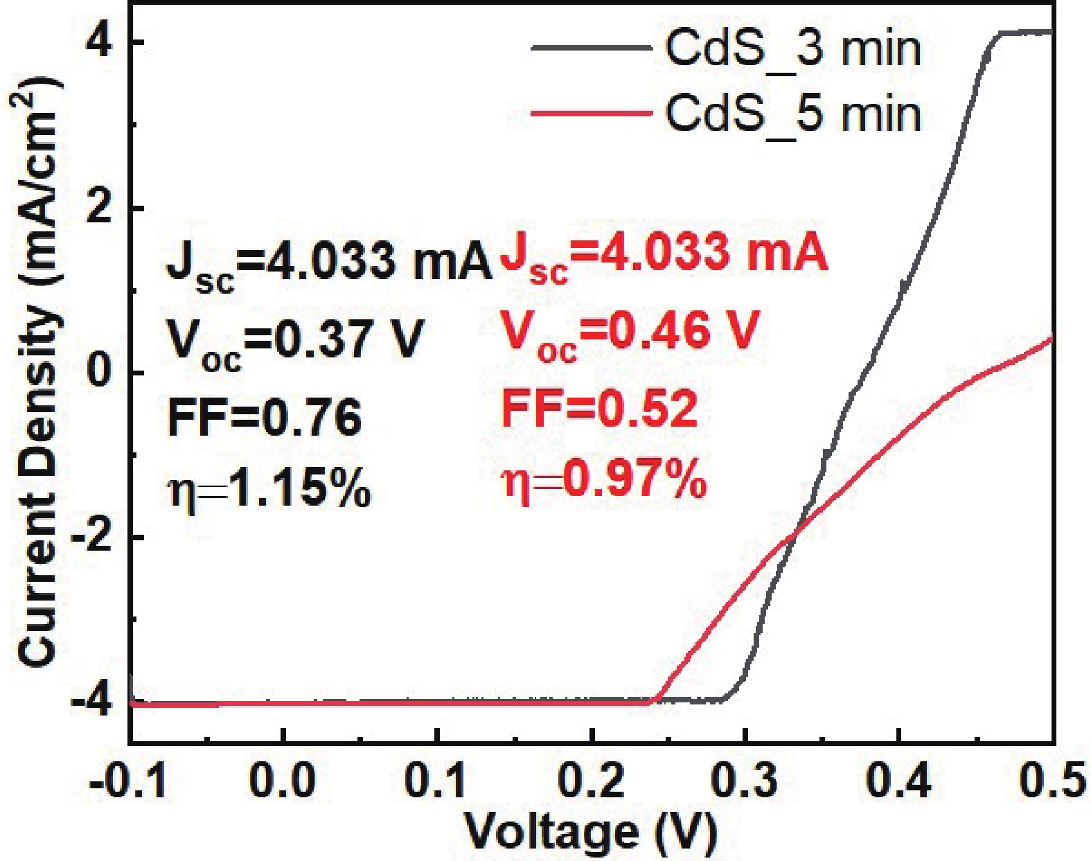

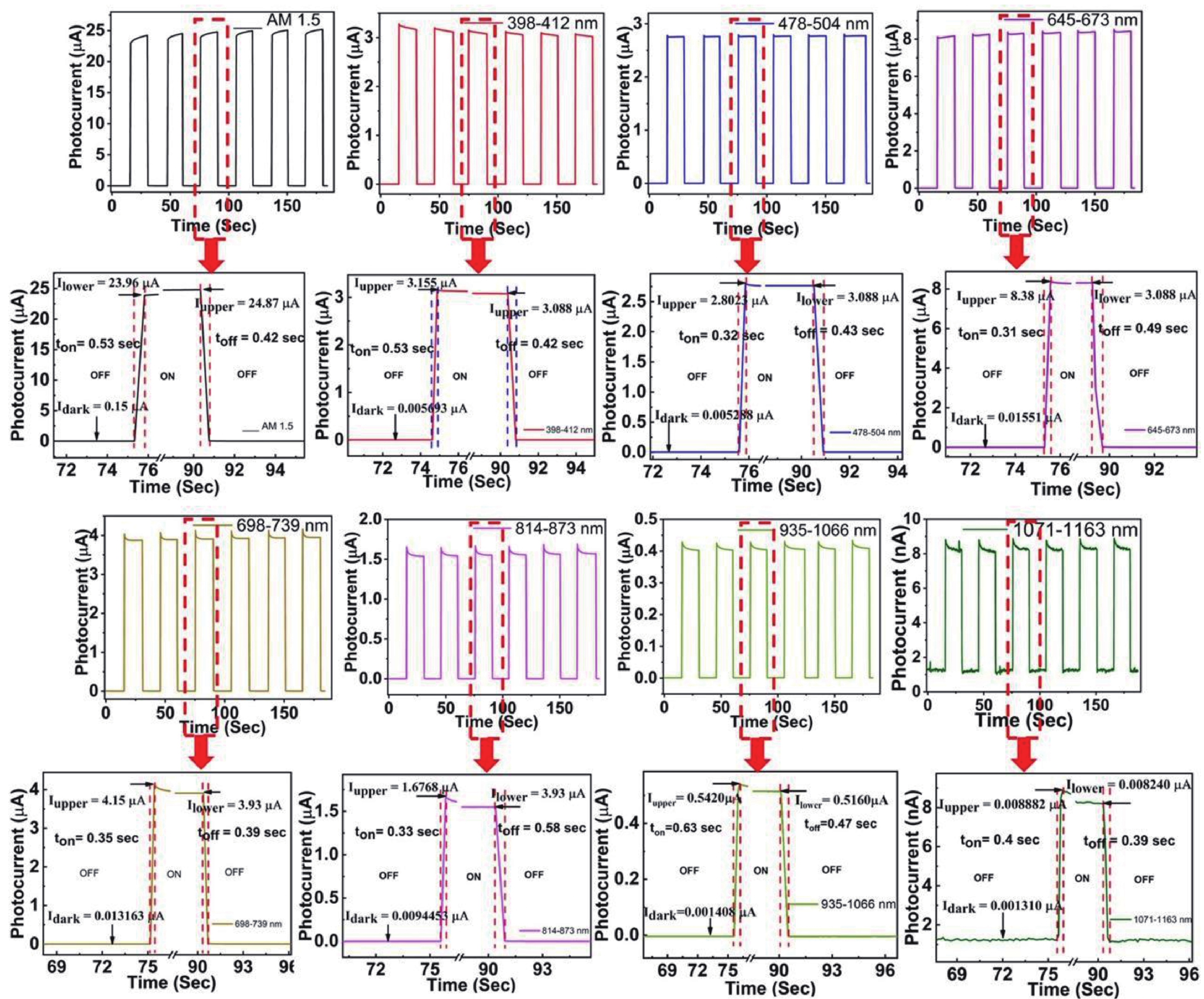
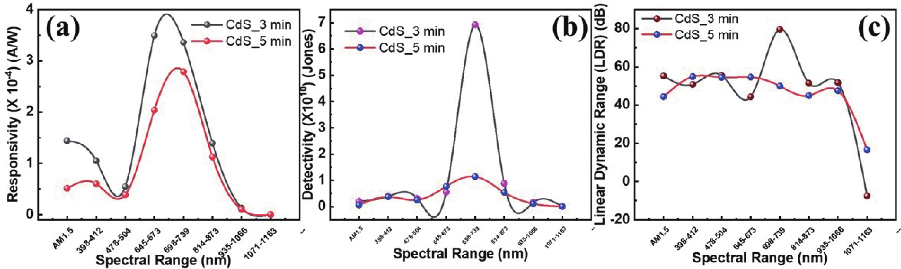
Table 1. Comparative review of work done on bifunctional capabilities of CZTS.
| Reference | Solar cell | Photodetector | ||||
| Efficiency (%) | Jsc (mA/cm2) | Voc (V) | Self-powered/biased | Detectivity (Jones) | ||
| Pesku et al.[36] | 2.82 | 20.80 | 0.46 | − | − | |
| Tumbul et al.[37] | 0.7 | 3.1 | 0.490 | − | − | |
| Gour et al.[38, 39] | − | − | − | Biasing (1mV) | 4.48 × 10⁸ | |
| Gour et al.[39] | − | − | − | Biasing (500 mV) | 109 | |
| This work | 1.15 | 4.037 | 0.37 | Self-powered | ~1010 | |
 DownLoad: CSV
Table 2. Growth parameters of Mo/CZTS thin films.
| Sample codes |
Mo (DC power) (W) |
CZTS (RF power) (W) |
RTP temp (°C) |
| A41 | 150 | 100 | 400 |
| A51 | 150 | 100 | 500 |
| A44 | 500 | 100 | 400 |
| A54 | 500 | 100 | 500 |
| B31 | 150 | 200 | 300 |
| B41 | 150 | 200 | 400 |
| B51 | 150 | 200 | 500 |
| B34 | 500 | 200 | 300 |
| B44 | 500 | 200 | 400 |
| B54 | 500 | 200 | 500 |
DownLoad: CSV
Table 3. Structural and electrical parameters of CZTS grown Mo coated SLG.
| Sample code | FWHM | Crystallite size (nm) | Dislocation density (nm−2) | Ideality factor | Schottky barrier height (eV) |
| A41 | 1.897 | 5.06 | 0.0391 | 1.94 | 0.63 |
| A44 | 1.552 | 5.82 | 0.0295 | 2.00 | 0.70 |
| A51 | 1.212 | 7.29 | 0.0188 | 2.00 | 0.62 |
| A54 | 0.921 | 10.04 | 0.0099 | 2.00 | 0.61 |
| B31 | 1.589 | 6.88 | 0.0211 | 2.00 | 0.62 |
| B34 | 7.206 | 5.54 | 0.0326 | 2.04 | 0.66 |
| B41 | 1.670 | 6.66 | 0.0225 | 2.00 | 0.61 |
| B44 | 1.746 | 6.56 | 0.0232 | 2.00 | 0.63 |
| B51 | 1.053 | 8.68 | 0.0133 | 2.00 | 0.62 |
| B54 | 1.388 | 8.75 | 0.0131 | 2.00 | 0.66 |
DownLoad: CSV
Table 4. Spectra range dependent photodetector parameters.
| Spectral range (nm) | Photocurrent ($ \mu {\rm{A}} $) | Responsivity (10−4 A/W) | Detectivity (109 Jones) | Linear dynamic range (dB) | |||||||
| 3 min | 5 min | 3 min | 5 min | 3 min | 5 min | 3 min | 5 min | ||||
| AM1.5 | 69.54 | 24.87 | 1.44 | 0.515 | 1.962 | 0.626 | 55.30 | 44.39 | |||
| 398−412 | 5.50 | 3.16 | 1.05 | 0.602 | 3.926 | 3.752 | 50.83 | 54.87 | |||
| 478−504 | 3.95 | 2.80 | 0.55 | 0.388 | 3.161 | 2.509 | 55.52 | 54.48 | |||
| 645−673 | 14.35 | 8.38 | 3.49 | 2.039 | 5.581 | 7.704 | 44.38 | 54.65 | |||
| 698−739 | 5.00 | 4.15 | 3.36 | 2.788 | 69.198 | 11.437 | 79.63 | 49.97 | |||
| 814−873 | 2.08 | 1.68 | 1.39 | 1.127 | 8.801 | 5.455 | 51.44 | 44.99 | |||
| 935−1066 | 0.54 | 0.43 | 0.13 | 0.103 | 1.626 | 1.140 | 51.71 | 47.55 | |||
| 1071−1163 | 0.0016 | 0.0089 | 0.0011 | 0.006 | 0.009 | 0.081 | 7.49 | 16.62 | |||
DownLoad: CSV
| [1] |
Prima E C, Rahmat A D, Setiawan A. Synthesis and fabrication of superstrate and substrate Cu2ZnSnS4/CdS thin film solar cells utilizing copper powder as local materials. J Ris Kaji Pendidik Fis, 2023, 10(1): 28 doi: 10.12928/jrkpf.v10i1.234
|
| [2] |
Islam M F, Md Yatim N, Hashim M A. A review of CZTS thin film solar cell technology. J Adv Res Fluid Mech Therm Sci, 2021, 81(1): 73 doi: 10.37934/arfmts.81.1.7387
|
| [3] |
Pramanik S, Trejo N, Mclntire E, et al. Transformations and environmental impacts of copper zinc tin sulfide nanoparticles and thin films. ACS Appl Mater Interfaces, 2023, 15(20): 24978 doi: 10.1021/acsami.3c00374
|
| [4] |
Rondiya S, Jadhav Y, Nasane M, et al. Interface structure and band alignment of CZTS/CdS heterojunction: An experimental and first-principles DFT investigation. Materials, 2019, 12(24): 4040 doi: 10.3390/ma12244040
|
| [5] |
Shimamune Y, Inoue S, Jimbo K. CZTS polycrystal formation by laser annealing and demonstration of solar cell fabrication. Jpn J Appl Phys, 2022, 61: SB1020 doi: 10.35848/1347-4065/ac290d
|
| [6] |
Lie S, Guc M, Tunuguntla V, et al. Comprehensive physicochemical and photovoltaic analysis of different Zn substitutes (Mn, Mg, Fe, Ni, Co, Ba, Sr) in CZTS-inspired thin film solar cells. J Mater Chem A, 2022, 10(16): 9137 doi: 10.1039/D2TA00225F
|
| [7] |
Zakaria S, El Mahboub E, El Hichou A. Physical properties of the low-cost CZTS absorber layer deposited by spin-coating: Effect of the copper concentration associated with SCAPS-1D simulation. RSC Adv, 2023, 13(39): 27106 doi: 10.1039/D3RA03996J
|
| [8] |
Martinho F, Hajijafarassar A, Lopez-Marino S, et al. Nitride-based interfacial layers for monolithic tandem integration of new solar energy materials on Si: The case of CZTS. ACS Appl Energy Mater, 2020, 3(5): 4600 doi: 10.1021/acsaem.0c00280
|
| [9] |
Zaki M Y, Velea A. Recent progress and challenges in controlling secondary phases in kesterite CZT(S/Se) thin films: A critical review. Energies, 2024, 17(7): 1600 doi: 10.3390/en17071600
|
| [10] |
Zaki M Y, Sava F, Buruiana A T, et al. Synthesis and characterization of Cu2ZnSnS4 thin films obtained by combined magnetron sputtering and pulsed laser deposition. Nanomaterials, 2021, 11(9): 2403 doi: 10.3390/nano11092403
|
| [11] |
Nazligul A S, Wang M Q, Choy K L. Recent development in earth-abundant kesterite materials and their applications. Sustainability, 2020, 12(12): 5138 doi: 10.3390/su12125138
|
| [12] |
Adewale Busari R, Alade Taleatu B, Adekunle Adewinbi S, et al. Surface characterisation of spin coated quaternary chalcogenide CZT(S, O) thin film for optoelectronic applications. J Photonic Mater Technol, 2019, 5(2): 38 doi: 10.11648/j.jmpt.20190502.13
|
| [13] |
Jayakumar A, Krishnan A. Electrodeposited CZTS loaded titania nanotubes for photocatalytic water splitting. IOP Conf Ser: Mater Sci Eng, 2023, 1291(1): 012006 doi: 10.1088/1757-899X/1291/1/012006
|
| [14] |
Raj C S A, Sebastian S, Susai Rajendran et al. A review on Spray pyrolysis deposited CZTS thin films for solar cell applications. J Univ Shanghai Sci Technol, 2021, 23(9): 1196 doi: 10.51201/JUSST/21/09681
|
| [15] |
Ikram A, Zulfequar M. Visible light driven CZTS QDs/α-Fe2O3-graphene p-n heterojunction for photoelectrochemical water splitting. Nanotechnology, 2023, 34(31): 315403 doi: 10.1088/1361-6528/acd1f3
|
| [16] |
Havryliuk Y, Dzhagan V, Karnaukhov A, et al. Influence of thermal and flash-lamp annealing on the thermoelectrical properties of Cu2ZnSnS4 nanocrystals obtained by green colloidal synthesis. Nanomaterials, 2023, 13(11): 1775 doi: 10.3390/nano13111775
|
| [17] |
Havryliuk Y, Dzhagan V, Karnaukhov A, et al. Raman spectroscopy and thermoelectric characterization of composite thin films of Cu2ZnSnS4 nanocrystals embedded in a conductive polymer PEDOT: PSS. Nanomaterials, 2022, 13(1): 41 doi: 10.3390/nano13010041
|
| [18] |
Zaki M Y, Sava F, Simandan I D, et al. A two-step magnetron sputtering approach for the synthesis of Cu2ZnSnS4 films from Cu2SnS3\ZnS stacks. ACS Omega, 2022, 7(27): 23800 doi: 10.1021/acsomega.2c02475
|
| [19] |
Krishnan A, Rishad Ali K, Vishnu G, et al. Towards phase pure CZTS thin films by SILAR method with augmented Zn adsorption for photovoltaic applications. Mater Renew Sustain Energy, 2019, 8(3): 16 doi: 10.1007/s40243-019-0152-1
|
| [20] |
Zhang X F, Fu E G, Wang Y H, et al. Fabrication of Cu2ZnSnS4 (CZTS) nanoparticle inks for growth of CZTS films for solar cells. Nanomaterials, 2019, 9(3): 336 doi: 10.3390/nano9030336
|
| [21] |
Patil S S, Nadaf S N, Mali S S, et al. Optoelectronic and photovoltaic properties of the Cu2ZnSnS4 photocathode by a temperature-dependent facile hydrothermal route. Ind Eng Chem Res, 2021, 60(21): 7816 doi: 10.1021/acs.iecr.1c00801
|
| [22] |
Mkawi E M, Al-Hadeethi Y, Arkook B, et al. Impact of 1, 8-diiodooctane (DIO) additive on the active layer properties of Cu2ZnSnS4 kesterite thin films prepared by electrochemical deposition for photovoltaic applications. Materials, 2023, 16(4): 1659 doi: 10.3390/ma16041659
|
| [23] |
Al-Hadeethi Y, Mkawi E M, Al-Hartomy, et al. role of triethanolamine in forming Cu2ZnSnS4 nanoparticles during solvothermal processing for solar cell applications. Int J Energy Res, 2022, 46: 7239 doi: 10.1002/er.7632
|
| [24] |
Cao V M H, Bae J, Shim J, et al. Fabrication of the Cu2ZnSnS4 thin film solar cell via a photo-sintering technique. Appl Sci, 2022, 12(1): 38 doi: 10.3390/app12010038
|
| [25] |
Wu T, Hu J G, Chen S, et al. Energy band alignment by solution-processed aluminum doping strategy toward record efficiency in pulsed laser-deposited kesterite thin-film solar cell. ACS Appl Mater Interfaces, 2023, 15(11): 14291 doi: 10.1021/acsami.2c22174
|
| [26] |
Ahmad A A, Migdadi A B, Alsaad A M, et al. Computational and experimental characterizations of annealed Cu2ZnSnS4 thin films. Heliyon, 2022, 8(1): e08683 doi: 10.1016/j.heliyon.2021.e08683
|
| [27] |
Huang L, Wang S J, Zhong L, et al. Role of ZnS particles in the performance of Cu2ZnSnS4 thin film solar cells: A comparative study by active control of zinc deposition in coevaporated precursors. Sol RRL, 2020, 4(11): 2000334 doi: 10.1002/solr.202000334
|
| [28] |
Shkir M, Khan M T, Ashraf I M, et al. High-performance visible light photodetectors based on inorganic CZT and InCZT single crystals. Sci Rep, 2019, 9(1): 12436 doi: 10.1038/s41598-019-48621-3
|
| [29] |
Wu D, Guo J W, Du J, et al. Highly polarization-sensitive, broadband, self-powered photodetector based on graphene/PdSe2/germanium heterojunction. ACS Nano, 2019, 13(9): 9907 doi: 10.1021/acsnano.9b03994
|
| [30] |
Ghods S, Vardast S, Esfandiar A, et al. Enhanced broadband photoresponsivity of the CZTS/WSe2 heterojunction by gate voltage. ACS Appl Electron Mater, 2022, 4(12): 6204 doi: 10.1021/acsaelm.2c01337
|
| [31] |
Wu H Z, Ma C H, Zhang J Y, et al. High-performance photodetectors with an ultrahigh photoswitching ratio and a very fast response speed in self-powered Cu2ZnSnS4/CdS PN heterojunctions. ACS Appl Electron Mater, 2021, 3(9): 4135 doi: 10.1021/acsaelm.1c00597
|
| [32] |
Allawi N H, Al-Jawad S M H. Synthesis and assessment of the Mo/MoO3/CZTS/Ag diode fabricated by one-pot hydrothermal route: Impact of temperature. Eur Phys J Appl Phys, 2024, 99: 30 doi: 10.1051/epjap/2024230185
|
| [33] |
Allawi N H, Al-Jawad S M H. Facile growth of kesterite CZTS film by one-pot hydrothermal route using EDTA as complex agent for heterojunction solar cell applications: Influence of zinc concentration. Opt Quantum Electron, 2023, 55(12): 1089 doi: 10.1007/s11082-023-05319-1
|
| [34] |
Allawi N H, Al-Jawad S M H. Toward phase pure CZTS film-based solar cell prepared by the one-step hydrothermal method: Influence of copper concentration. ECS J Solid State Sci Technol, 2023, 12(7): 075001 doi: 10.1149/2162-8777/ace214
|
| [35] |
Allawi N H, Al-Jawad S M H. Cauliflower Cu2ZnSnS4: Na film prepared by single-pot hydrothermal approach for photovoltaic application: Impact of NaOH additive. J Appl Electrochem, 2024, 54(7): 1567 doi: 10.1007/s10800-023-02052-1
|
| [36] |
Peksu E, Karaagac H. Preparation of CZTS thin films for the fabrication of ZnO nanorods based superstrate solar cells. J Alloys Compd, 2021, 884: 161124 doi: 10.1016/j.jallcom.2021.161124
|
| [37] |
Tumbul A, Aslan F, Göktaş A, et al. All solution processed superstrate type Cu2ZnSnS4 (CZTS) thin film solar cell: Effect of absorber layer thickness. J Alloys Compd, 2019, 781: 280 doi: 10.1016/j.jallcom.2018.12.012
|
| [38] |
Gour K S, Bhattacharyya B, Singh O P, et al. Nanostructured Cu2ZnSnS4 (CZTS) thin film for self-powered broadband photodetection. J Alloys Compd, 2018, 735: 285 doi: 10.1016/j.jallcom.2017.11.079
|
| [39] |
Gour K S, Karade V, Pandey A, et al. High-speed, low-bias operated, broadband (Vis-NIR) photodetector based on sputtered Cu2ZnSn(S, Se)4 (CZTSSe) thin films. Sens Actuat A Phys, 2020, 314: 112231 doi: 10.1016/j.sna.2020.112231
|
| [40] |
Chavan K B, Desarada S V, Chaure S, et al. Study of substrate dependent microstructural properties of sputtered Mo/CZTS heterojunctions using X ray diffraction. Solid State Sci, 2024, 158: 107739 doi: 10.1016/j.solidstatesciences.2024.107739
|
| [41] |
Cullity B D. Elements of X ray diffraction. Pearson, 2014
|
| [42] |
Wiatrowski A, Obstarczyk A, Mazur M, et al. Characterization of HfO2 optical coatings deposited by MF magnetron sputtering. Coatings, 2019, 9(2): 106 doi: 10.3390/coatings9020106
|
| [43] |
Ghasemi S, Farhadizadeh A R, Ali Amadeh A, et al. Structural and morphological properties of TiN deposited by magnetron sputtering. Surf Topogr: Metrol Prop, 2018, 6(4): 045003 doi: 10.1088/2051-672X/aae405
|
| [44] |
Alaksanasuwan S, Buranawong A, Witit-Anun N. Effect of sputtering current on the structure of TiCrN thin films prepared from mosaic target by reactive DC magnetron sputtering. Appl Mech Mater, 2020, 901: 37 doi: 10.4028/www.scientific.net/AMM.901.37
|
| [45] |
Wang W K, Liu K F, Tsai P C, et al. Influence of annealing temperature on the properties of ZnGa2O4 thin films by magnetron sputtering. Coatings, 2019, 9(12): 859 doi: 10.3390/coatings9120859
|
| [46] |
Almohammedi A, Shaaban E R. Spectroscopic ellipsometry and photovoltaic characteristics for n-CdS/p-Cu2ZnSnS4 heterojunction by annealing for solar cells. Chalcogenide Lett, 2022, 19(10): 701 doi: 10.15251/CL.2022.1910.701
|
| [47] |
Chavan K B, Chaure N B. Studies on controlled preferentially orientated Mo thin films via sputtering technique. Mater Res Express, 2019, 6(7): 076423 doi: 10.1088/2053-1591/ab162d
|
| [48] |
Xu J X, Cao Z M, Yang Y Z, et al. Characterization of Cu2ZnSnS4 thin films on flexible metal foil substrates. J Mater Sci Mater Electron, 2015, 26(2): 726 doi: 10.1007/s10854-014-2456-3
|
| [49] |
Venugopal B, Shown I, Samireddi S, et al. Microstructural intra-granular cracking in Cu2ZnSnS4@C thin-film anode enhanced the electrochemical performance in lithium-ion battery applications. Mater Adv, 2021, 2(17): 5672 doi: 10.1039/D1MA00471A
|
| [50] |
Ataollahi N, Bazerla F, Malerba C, et al. Synthesis and post-annealing of Cu2ZnSnS4 absorber layers based on oleylamine/1-dodecanethiol. Materials, 2019, 12(20): 3320 doi: 10.3390/ma12203320
|
| [51] |
Almohammedi A, Ashour A, Essam R. Shaaban et al. Structural, morphological and optical properties of annealed Cu2ZnSnS4 thin films using the first derivative of tga curve for solar cell applications. J Ovonic Res, 2020, 16(1): 21 doi: 10.15251/JOR.2020.161.21
|
| [52] |
Selyshchev O, Havryliuk Y, Valakh M Y, et al. Raman and X-ray photoemission identification of colloidal metal sulfides as potential secondary phases in nanocrystalline Cu2ZnSnS4 photovoltaic absorbers. ACS Appl Nano Mater, 2020, 3(6): 5706 doi: 10.1021/acsanm.0c00910
|
| [53] |
Turkoglu F, Koseoglu H, Cantas A, et al. Effect of defects and secondary phases in Cu2ZnSnS4 absorber material on the performance of Zn(O, S) buffered devices. Thin Solid Films, 2019, 670: 6 doi: 10.1016/j.tsf.2018.12.001
|
| [54] |
Nguyen T H, Kawaguchi T, Chantana J, et al. Structural and solar cell properties of a Ag-containing Cu2ZnSnS4 thin film derived from spray pyrolysis. ACS Appl Mater Interfaces, 2018, 10(6): 5455 doi: 10.1021/acsami.7b14929
|
| [55] |
Sava F, Diagne O, Gâlcă A C, et al. Secondary crystalline phases influence on optical properties in off-stoichiometric Cu2S–ZnS–SnS2 thin films. Materials, 2020, 13(20): 4624 doi: 10.3390/ma13204624
|
| [56] |
Ahmad R, Saddiqi N, Wu M, et al. Effect of the counteranion on the formation pathway of Cu2ZnSnS4 (CZTS) nanoparticles under Solvothermal conditionsm. Inorg Chem, 2020, 59(3): 1973 doi: 10.1021/acs.inorgchem.9b03338
|
| [57] |
Chen J, Wang F C, Yang B B, et al. Fabrication of Cu2ZnSnS4 thin films based on facile nanocrystals-printing approach with rapid thermal annealing (RTA) process. Coatings, 2019, 9(2): 130 doi: 10.3390/coatings9020130
|
| [58] |
Baláž P, Hegedus M, Baláž M, et al. Photovoltaic materials: Cu2ZnSnS4 (CZTS) nanocrystals synthesized via industrially scalable, green, one-step mechanochemical process. Prog in Photovoltaics, 2019, 27(9): 798 doi: 10.1002/pip.3152
|
| [59] |
Pitale S, Ghosh M, Singh S G, et al. Characteristics of Al/Ge Schottky and ohmic contacts at low temperatures. Mater Sci Semicond Process, 2021, 130: 105820 doi: 10.1016/j.mssp.2021.105820
|
| [60] |
Nam Y, Yang J H, Jeong P, et al. Effect of a rapid thermal annealing process on the electrical properties of an aluminum-doped indium zinc tin oxide thin film transistor. Phys Status Solidi A, 2017, 214(1): 1600490 doi: 10.1002/pssa.201600490
|
| [61] |
Horng R H, Wuu D S, Chan S H, et al. Rapid-thermal-processed BaTiO3 thin films deposited by liquid-source misted chemical deposition. Jpn J Appl Phys, 1998, 37(3R): 885 doi: 10.1143/JJAP.37.885
|
| [62] |
Pérez R, Mestres N, Montserrat J, et al. Barrier inhomogeneities and electrical characteristics of Ni/Ti bilayer Schottky contacts on 4H-SiC after high temperature treatments. Phys Status Solidi Appl Res, 2005, 202(4): 692 doi: 10.1002/pssa.200460475
|
| [63] |
Lee S Y, Yun W S, Lee J D. New method to determine the Schottky barrier in few-layer black phosphorus metal contacts. ACS Appl Mater Interfaces, 2017, 9(8): 7873 doi: 10.1021/acsami.7b00357
|
| [64] |
White E R, Ashok S, Allara D L. Junction formation in silicon using a phosphorus vapor source and rapid thermal drive-In. MRS Online Proc Libr, 1992, 260(1): 265 doi: 10.1557/PROC-260-265
|
| [65] |
Zhang X F, Fu E G, Zheng M X, et al. Fabrication of Cu2ZnSnS4 thin films from ball-milled nanoparticle inks under various annealing temperatures. Nanomaterials, 2019, 9(11): 1615 doi: 10.3390/nano9111615
|
| [66] |
Ye F, He C S, Wu T, et al. Sputtering deposited and energy band matched ZnSnN2 buffer layers for highly efficient Cd-free Cu2ZnSnS4 solar cells. Adv Funct Materials, 2024, 34(38): 2402762 doi: 10.1002/adfm.202402762
|
| [67] |
Ismail Fathima M, Arulanantham A S, Joseph Wilson K S. Effect of ZnS nanowire ARC on CZTS/CdS thin film solar cell by Nebulizer spray pyrolysis technique. Mater Res Express, 2020, 7(1): 015510 doi: 10.1088/2053-1591/ab63f9
|
| [68] |
Platzer-Björkman C, Barreau N, Bär M, et al. Back and front contacts in kesterite solar cells: State-of-the-art and open questions. J Phys Energy, 2019, 1(4): 044005 doi: 10.1088/2515-7655/ab3708
|
| [69] |
Chu L L, Zhang J P, Xiang H W, et al. Synergetic effects of Zn alloying and defect engineering on improving the CdS buffer layer of Cu2ZnSnS4 solar cells. Inorg Chem, 2022, 61(31): 12293 doi: 10.1021/acs.inorgchem.2c01575
|
| [70] |
Yang X X, Liu X, Qu L H, et al. Boosting photoresponse of self-powered InSe-based photoelectrochemical photodetectors via suppression of interface doping. ACS Nano, 2022, 16(5): 8440 doi: 10.1021/acsnano.2c02986
|
| [71] |
Sorifi S, Moun M, Kaushik S, et al. 2020 high-temperature performance of a GaSe nanosheet-based broadband photodetector. ACS Appl Electron Mater, 2020, 2(3): 670 doi: 10.1021/acsaelm.9b00770
|
| [72] |
Shao D L, Zhu W G, Liu X Q, et al. Ultrasensitive UV photodetector based on interfacial charge-controlled inorganic perovskite-polymer hybrid structure. ACS Appl Mater Interfaces, 2020, 12(38): 43106 doi: 10.1021/acsami.0c09890
|
| [73] |
Xin J, Wang Q, Li J H, et al. Planar visible–near infrared photodetectors based on organic–inorganic hybrid perovskite single crystal bulks. J Phys D Appl Phys, 2017, 53: 414003 doi: 10.1088/1361-6463/ab94e510.1088/1361-6463/ab94e5
|
| [74] |
Zhou S. 2024 PtTe2/WS2/Pyramidal-Si Van Der Waals heterojunction with semiconformal interfaces toward high-performance photodetectors. ACS Photonics, 2024, 11(4): 1810-20 doi: 10.1021/acsphotonics.4c00331
|
| [75] |
Yang T F, Wang X, Zheng B Y, et al. Ultrahigh-performance optoelectronics demonstrated in ultrathin perovskite-based vertical semiconductor heterostructures. ACS Nano, 2019, 13(7): 7996 doi: 10.1021/acsnano.9b02676
|


Article views: 1025 Times PDF downloads: 160 Times Cited by: 0 Times
Received: 13 March 2025 Revised: 14 May 2025 Online: Accepted Manuscript: 15 July 2025Uncorrected proof: 13 August 2025Published: 15 January 2026
| Citation: |
Kalyan B. Chavan, Maruti V. Salve, Shweta Chaure, Nandu B. Chaure. CZTS based novel bifunctional photovoltaic and self-powered photodetection nano system[J]. Journal of Semiconductors, 2026, 47(1): 012401. doi: 10.1088/1674-4926/25030025
****
Kalyan B. Chavan, M V Salve, S Chaure, and N B Chaure, CZTS based novel bifunctional photovoltaic and self-powered photodetection nano system[J]. J. Semicond., 2026, 47(1): 012401 doi: 10.1088/1674-4926/25030025

|
 Kalyan B. Chavan is a research scholar at the Savitribai Phule Pune University in Pune, India. He earned his M.Sc. from the University of Pune, India. He is currently working on his Ph.D. in RF sputtered CZTS-based thin film solar cells under the guidance of Prof. Nandu B. Chaure. Aside from this, he works in a variety of scientific fields, including semiconductor physics, energy materials for thin film photovoltaics, and supercapacitor applications
 Nandu B. Chaure is a Professor at Savitribai Phule Pune University, Pune, India. He received his M.Sc. and Ph.D. in Materials and Device Physics from the University of Pune and University of Bhopal, India. His research mainly focuses on Semiconductor Physics, Energy materials for thin film photovoltaics and supercapacitor applications
| [1] |
Prima E C, Rahmat A D, Setiawan A. Synthesis and fabrication of superstrate and substrate Cu2ZnSnS4/CdS thin film solar cells utilizing copper powder as local materials. J Ris Kaji Pendidik Fis, 2023, 10(1): 28 doi: 10.12928/jrkpf.v10i1.234
|
| [2] |
Islam M F, Md Yatim N, Hashim M A. A review of CZTS thin film solar cell technology. J Adv Res Fluid Mech Therm Sci, 2021, 81(1): 73 doi: 10.37934/arfmts.81.1.7387
|
| [3] |
Pramanik S, Trejo N, Mclntire E, et al. Transformations and environmental impacts of copper zinc tin sulfide nanoparticles and thin films. ACS Appl Mater Interfaces, 2023, 15(20): 24978 doi: 10.1021/acsami.3c00374
|
| [4] |
Rondiya S, Jadhav Y, Nasane M, et al. Interface structure and band alignment of CZTS/CdS heterojunction: An experimental and first-principles DFT investigation. Materials, 2019, 12(24): 4040 doi: 10.3390/ma12244040
|
| [5] |
Shimamune Y, Inoue S, Jimbo K. CZTS polycrystal formation by laser annealing and demonstration of solar cell fabrication. Jpn J Appl Phys, 2022, 61: SB1020 doi: 10.35848/1347-4065/ac290d
|
| [6] |
Lie S, Guc M, Tunuguntla V, et al. Comprehensive physicochemical and photovoltaic analysis of different Zn substitutes (Mn, Mg, Fe, Ni, Co, Ba, Sr) in CZTS-inspired thin film solar cells. J Mater Chem A, 2022, 10(16): 9137 doi: 10.1039/D2TA00225F
|
| [7] |
Zakaria S, El Mahboub E, El Hichou A. Physical properties of the low-cost CZTS absorber layer deposited by spin-coating: Effect of the copper concentration associated with SCAPS-1D simulation. RSC Adv, 2023, 13(39): 27106 doi: 10.1039/D3RA03996J
|
| [8] |
Martinho F, Hajijafarassar A, Lopez-Marino S, et al. Nitride-based interfacial layers for monolithic tandem integration of new solar energy materials on Si: The case of CZTS. ACS Appl Energy Mater, 2020, 3(5): 4600 doi: 10.1021/acsaem.0c00280
|
| [9] |
Zaki M Y, Velea A. Recent progress and challenges in controlling secondary phases in kesterite CZT(S/Se) thin films: A critical review. Energies, 2024, 17(7): 1600 doi: 10.3390/en17071600
|
| [10] |
Zaki M Y, Sava F, Buruiana A T, et al. Synthesis and characterization of Cu2ZnSnS4 thin films obtained by combined magnetron sputtering and pulsed laser deposition. Nanomaterials, 2021, 11(9): 2403 doi: 10.3390/nano11092403
|
| [11] |
Nazligul A S, Wang M Q, Choy K L. Recent development in earth-abundant kesterite materials and their applications. Sustainability, 2020, 12(12): 5138 doi: 10.3390/su12125138
|
| [12] |
Adewale Busari R, Alade Taleatu B, Adekunle Adewinbi S, et al. Surface characterisation of spin coated quaternary chalcogenide CZT(S, O) thin film for optoelectronic applications. J Photonic Mater Technol, 2019, 5(2): 38 doi: 10.11648/j.jmpt.20190502.13
|
| [13] |
Jayakumar A, Krishnan A. Electrodeposited CZTS loaded titania nanotubes for photocatalytic water splitting. IOP Conf Ser: Mater Sci Eng, 2023, 1291(1): 012006 doi: 10.1088/1757-899X/1291/1/012006
|
| [14] |
Raj C S A, Sebastian S, Susai Rajendran et al. A review on Spray pyrolysis deposited CZTS thin films for solar cell applications. J Univ Shanghai Sci Technol, 2021, 23(9): 1196 doi: 10.51201/JUSST/21/09681
|
| [15] |
Ikram A, Zulfequar M. Visible light driven CZTS QDs/α-Fe2O3-graphene p-n heterojunction for photoelectrochemical water splitting. Nanotechnology, 2023, 34(31): 315403 doi: 10.1088/1361-6528/acd1f3
|
| [16] |
Havryliuk Y, Dzhagan V, Karnaukhov A, et al. Influence of thermal and flash-lamp annealing on the thermoelectrical properties of Cu2ZnSnS4 nanocrystals obtained by green colloidal synthesis. Nanomaterials, 2023, 13(11): 1775 doi: 10.3390/nano13111775
|
| [17] |
Havryliuk Y, Dzhagan V, Karnaukhov A, et al. Raman spectroscopy and thermoelectric characterization of composite thin films of Cu2ZnSnS4 nanocrystals embedded in a conductive polymer PEDOT: PSS. Nanomaterials, 2022, 13(1): 41 doi: 10.3390/nano13010041
|
| [18] |
Zaki M Y, Sava F, Simandan I D, et al. A two-step magnetron sputtering approach for the synthesis of Cu2ZnSnS4 films from Cu2SnS3\ZnS stacks. ACS Omega, 2022, 7(27): 23800 doi: 10.1021/acsomega.2c02475
|
| [19] |
Krishnan A, Rishad Ali K, Vishnu G, et al. Towards phase pure CZTS thin films by SILAR method with augmented Zn adsorption for photovoltaic applications. Mater Renew Sustain Energy, 2019, 8(3): 16 doi: 10.1007/s40243-019-0152-1
|
| [20] |
Zhang X F, Fu E G, Wang Y H, et al. Fabrication of Cu2ZnSnS4 (CZTS) nanoparticle inks for growth of CZTS films for solar cells. Nanomaterials, 2019, 9(3): 336 doi: 10.3390/nano9030336
|
| [21] |
Patil S S, Nadaf S N, Mali S S, et al. Optoelectronic and photovoltaic properties of the Cu2ZnSnS4 photocathode by a temperature-dependent facile hydrothermal route. Ind Eng Chem Res, 2021, 60(21): 7816 doi: 10.1021/acs.iecr.1c00801
|
| [22] |
Mkawi E M, Al-Hadeethi Y, Arkook B, et al. Impact of 1, 8-diiodooctane (DIO) additive on the active layer properties of Cu2ZnSnS4 kesterite thin films prepared by electrochemical deposition for photovoltaic applications. Materials, 2023, 16(4): 1659 doi: 10.3390/ma16041659
|
| [23] |
Al-Hadeethi Y, Mkawi E M, Al-Hartomy, et al. role of triethanolamine in forming Cu2ZnSnS4 nanoparticles during solvothermal processing for solar cell applications. Int J Energy Res, 2022, 46: 7239 doi: 10.1002/er.7632
|
| [24] |
Cao V M H, Bae J, Shim J, et al. Fabrication of the Cu2ZnSnS4 thin film solar cell via a photo-sintering technique. Appl Sci, 2022, 12(1): 38 doi: 10.3390/app12010038
|
| [25] |
Wu T, Hu J G, Chen S, et al. Energy band alignment by solution-processed aluminum doping strategy toward record efficiency in pulsed laser-deposited kesterite thin-film solar cell. ACS Appl Mater Interfaces, 2023, 15(11): 14291 doi: 10.1021/acsami.2c22174
|
| [26] |
Ahmad A A, Migdadi A B, Alsaad A M, et al. Computational and experimental characterizations of annealed Cu2ZnSnS4 thin films. Heliyon, 2022, 8(1): e08683 doi: 10.1016/j.heliyon.2021.e08683
|
| [27] |
Huang L, Wang S J, Zhong L, et al. Role of ZnS particles in the performance of Cu2ZnSnS4 thin film solar cells: A comparative study by active control of zinc deposition in coevaporated precursors. Sol RRL, 2020, 4(11): 2000334 doi: 10.1002/solr.202000334
|
| [28] |
Shkir M, Khan M T, Ashraf I M, et al. High-performance visible light photodetectors based on inorganic CZT and InCZT single crystals. Sci Rep, 2019, 9(1): 12436 doi: 10.1038/s41598-019-48621-3
|
| [29] |
Wu D, Guo J W, Du J, et al. Highly polarization-sensitive, broadband, self-powered photodetector based on graphene/PdSe2/germanium heterojunction. ACS Nano, 2019, 13(9): 9907 doi: 10.1021/acsnano.9b03994
|
| [30] |
Ghods S, Vardast S, Esfandiar A, et al. Enhanced broadband photoresponsivity of the CZTS/WSe2 heterojunction by gate voltage. ACS Appl Electron Mater, 2022, 4(12): 6204 doi: 10.1021/acsaelm.2c01337
|
| [31] |
Wu H Z, Ma C H, Zhang J Y, et al. High-performance photodetectors with an ultrahigh photoswitching ratio and a very fast response speed in self-powered Cu2ZnSnS4/CdS PN heterojunctions. ACS Appl Electron Mater, 2021, 3(9): 4135 doi: 10.1021/acsaelm.1c00597
|
| [32] |
Allawi N H, Al-Jawad S M H. Synthesis and assessment of the Mo/MoO3/CZTS/Ag diode fabricated by one-pot hydrothermal route: Impact of temperature. Eur Phys J Appl Phys, 2024, 99: 30 doi: 10.1051/epjap/2024230185
|
| [33] |
Allawi N H, Al-Jawad S M H. Facile growth of kesterite CZTS film by one-pot hydrothermal route using EDTA as complex agent for heterojunction solar cell applications: Influence of zinc concentration. Opt Quantum Electron, 2023, 55(12): 1089 doi: 10.1007/s11082-023-05319-1
|
| [34] |
Allawi N H, Al-Jawad S M H. Toward phase pure CZTS film-based solar cell prepared by the one-step hydrothermal method: Influence of copper concentration. ECS J Solid State Sci Technol, 2023, 12(7): 075001 doi: 10.1149/2162-8777/ace214
|
| [35] |
Allawi N H, Al-Jawad S M H. Cauliflower Cu2ZnSnS4: Na film prepared by single-pot hydrothermal approach for photovoltaic application: Impact of NaOH additive. J Appl Electrochem, 2024, 54(7): 1567 doi: 10.1007/s10800-023-02052-1
|
| [36] |
Peksu E, Karaagac H. Preparation of CZTS thin films for the fabrication of ZnO nanorods based superstrate solar cells. J Alloys Compd, 2021, 884: 161124 doi: 10.1016/j.jallcom.2021.161124
|
| [37] |
Tumbul A, Aslan F, Göktaş A, et al. All solution processed superstrate type Cu2ZnSnS4 (CZTS) thin film solar cell: Effect of absorber layer thickness. J Alloys Compd, 2019, 781: 280 doi: 10.1016/j.jallcom.2018.12.012
|
| [38] |
Gour K S, Bhattacharyya B, Singh O P, et al. Nanostructured Cu2ZnSnS4 (CZTS) thin film for self-powered broadband photodetection. J Alloys Compd, 2018, 735: 285 doi: 10.1016/j.jallcom.2017.11.079
|
| [39] |
Gour K S, Karade V, Pandey A, et al. High-speed, low-bias operated, broadband (Vis-NIR) photodetector based on sputtered Cu2ZnSn(S, Se)4 (CZTSSe) thin films. Sens Actuat A Phys, 2020, 314: 112231 doi: 10.1016/j.sna.2020.112231
|
| [40] |
Chavan K B, Desarada S V, Chaure S, et al. Study of substrate dependent microstructural properties of sputtered Mo/CZTS heterojunctions using X ray diffraction. Solid State Sci, 2024, 158: 107739 doi: 10.1016/j.solidstatesciences.2024.107739
|
| [41] |
Cullity B D. Elements of X ray diffraction. Pearson, 2014
|
| [42] |
Wiatrowski A, Obstarczyk A, Mazur M, et al. Characterization of HfO2 optical coatings deposited by MF magnetron sputtering. Coatings, 2019, 9(2): 106 doi: 10.3390/coatings9020106
|
| [43] |
Ghasemi S, Farhadizadeh A R, Ali Amadeh A, et al. Structural and morphological properties of TiN deposited by magnetron sputtering. Surf Topogr: Metrol Prop, 2018, 6(4): 045003 doi: 10.1088/2051-672X/aae405
|
| [44] |
Alaksanasuwan S, Buranawong A, Witit-Anun N. Effect of sputtering current on the structure of TiCrN thin films prepared from mosaic target by reactive DC magnetron sputtering. Appl Mech Mater, 2020, 901: 37 doi: 10.4028/www.scientific.net/AMM.901.37
|
| [45] |
Wang W K, Liu K F, Tsai P C, et al. Influence of annealing temperature on the properties of ZnGa2O4 thin films by magnetron sputtering. Coatings, 2019, 9(12): 859 doi: 10.3390/coatings9120859
|
| [46] |
Almohammedi A, Shaaban E R. Spectroscopic ellipsometry and photovoltaic characteristics for n-CdS/p-Cu2ZnSnS4 heterojunction by annealing for solar cells. Chalcogenide Lett, 2022, 19(10): 701 doi: 10.15251/CL.2022.1910.701
|
| [47] |
Chavan K B, Chaure N B. Studies on controlled preferentially orientated Mo thin films via sputtering technique. Mater Res Express, 2019, 6(7): 076423 doi: 10.1088/2053-1591/ab162d
|
| [48] |
Xu J X, Cao Z M, Yang Y Z, et al. Characterization of Cu2ZnSnS4 thin films on flexible metal foil substrates. J Mater Sci Mater Electron, 2015, 26(2): 726 doi: 10.1007/s10854-014-2456-3
|
| [49] |
Venugopal B, Shown I, Samireddi S, et al. Microstructural intra-granular cracking in Cu2ZnSnS4@C thin-film anode enhanced the electrochemical performance in lithium-ion battery applications. Mater Adv, 2021, 2(17): 5672 doi: 10.1039/D1MA00471A
|
| [50] |
Ataollahi N, Bazerla F, Malerba C, et al. Synthesis and post-annealing of Cu2ZnSnS4 absorber layers based on oleylamine/1-dodecanethiol. Materials, 2019, 12(20): 3320 doi: 10.3390/ma12203320
|
| [51] |
Almohammedi A, Ashour A, Essam R. Shaaban et al. Structural, morphological and optical properties of annealed Cu2ZnSnS4 thin films using the first derivative of tga curve for solar cell applications. J Ovonic Res, 2020, 16(1): 21 doi: 10.15251/JOR.2020.161.21
|
| [52] |
Selyshchev O, Havryliuk Y, Valakh M Y, et al. Raman and X-ray photoemission identification of colloidal metal sulfides as potential secondary phases in nanocrystalline Cu2ZnSnS4 photovoltaic absorbers. ACS Appl Nano Mater, 2020, 3(6): 5706 doi: 10.1021/acsanm.0c00910
|
| [53] |
Turkoglu F, Koseoglu H, Cantas A, et al. Effect of defects and secondary phases in Cu2ZnSnS4 absorber material on the performance of Zn(O, S) buffered devices. Thin Solid Films, 2019, 670: 6 doi: 10.1016/j.tsf.2018.12.001
|
| [54] |
Nguyen T H, Kawaguchi T, Chantana J, et al. Structural and solar cell properties of a Ag-containing Cu2ZnSnS4 thin film derived from spray pyrolysis. ACS Appl Mater Interfaces, 2018, 10(6): 5455 doi: 10.1021/acsami.7b14929
|
| [55] |
Sava F, Diagne O, Gâlcă A C, et al. Secondary crystalline phases influence on optical properties in off-stoichiometric Cu2S–ZnS–SnS2 thin films. Materials, 2020, 13(20): 4624 doi: 10.3390/ma13204624
|
| [56] |
Ahmad R, Saddiqi N, Wu M, et al. Effect of the counteranion on the formation pathway of Cu2ZnSnS4 (CZTS) nanoparticles under Solvothermal conditionsm. Inorg Chem, 2020, 59(3): 1973 doi: 10.1021/acs.inorgchem.9b03338
|
| [57] |
Chen J, Wang F C, Yang B B, et al. Fabrication of Cu2ZnSnS4 thin films based on facile nanocrystals-printing approach with rapid thermal annealing (RTA) process. Coatings, 2019, 9(2): 130 doi: 10.3390/coatings9020130
|
| [58] |
Baláž P, Hegedus M, Baláž M, et al. Photovoltaic materials: Cu2ZnSnS4 (CZTS) nanocrystals synthesized via industrially scalable, green, one-step mechanochemical process. Prog in Photovoltaics, 2019, 27(9): 798 doi: 10.1002/pip.3152
|
| [59] |
Pitale S, Ghosh M, Singh S G, et al. Characteristics of Al/Ge Schottky and ohmic contacts at low temperatures. Mater Sci Semicond Process, 2021, 130: 105820 doi: 10.1016/j.mssp.2021.105820
|
| [60] |
Nam Y, Yang J H, Jeong P, et al. Effect of a rapid thermal annealing process on the electrical properties of an aluminum-doped indium zinc tin oxide thin film transistor. Phys Status Solidi A, 2017, 214(1): 1600490 doi: 10.1002/pssa.201600490
|
| [61] |
Horng R H, Wuu D S, Chan S H, et al. Rapid-thermal-processed BaTiO3 thin films deposited by liquid-source misted chemical deposition. Jpn J Appl Phys, 1998, 37(3R): 885 doi: 10.1143/JJAP.37.885
|
| [62] |
Pérez R, Mestres N, Montserrat J, et al. Barrier inhomogeneities and electrical characteristics of Ni/Ti bilayer Schottky contacts on 4H-SiC after high temperature treatments. Phys Status Solidi Appl Res, 2005, 202(4): 692 doi: 10.1002/pssa.200460475
|
| [63] |
Lee S Y, Yun W S, Lee J D. New method to determine the Schottky barrier in few-layer black phosphorus metal contacts. ACS Appl Mater Interfaces, 2017, 9(8): 7873 doi: 10.1021/acsami.7b00357
|
| [64] |
White E R, Ashok S, Allara D L. Junction formation in silicon using a phosphorus vapor source and rapid thermal drive-In. MRS Online Proc Libr, 1992, 260(1): 265 doi: 10.1557/PROC-260-265
|
| [65] |
Zhang X F, Fu E G, Zheng M X, et al. Fabrication of Cu2ZnSnS4 thin films from ball-milled nanoparticle inks under various annealing temperatures. Nanomaterials, 2019, 9(11): 1615 doi: 10.3390/nano9111615
|
| [66] |
Ye F, He C S, Wu T, et al. Sputtering deposited and energy band matched ZnSnN2 buffer layers for highly efficient Cd-free Cu2ZnSnS4 solar cells. Adv Funct Materials, 2024, 34(38): 2402762 doi: 10.1002/adfm.202402762
|
| [67] |
Ismail Fathima M, Arulanantham A S, Joseph Wilson K S. Effect of ZnS nanowire ARC on CZTS/CdS thin film solar cell by Nebulizer spray pyrolysis technique. Mater Res Express, 2020, 7(1): 015510 doi: 10.1088/2053-1591/ab63f9
|
| [68] |
Platzer-Björkman C, Barreau N, Bär M, et al. Back and front contacts in kesterite solar cells: State-of-the-art and open questions. J Phys Energy, 2019, 1(4): 044005 doi: 10.1088/2515-7655/ab3708
|
| [69] |
Chu L L, Zhang J P, Xiang H W, et al. Synergetic effects of Zn alloying and defect engineering on improving the CdS buffer layer of Cu2ZnSnS4 solar cells. Inorg Chem, 2022, 61(31): 12293 doi: 10.1021/acs.inorgchem.2c01575
|
| [70] |
Yang X X, Liu X, Qu L H, et al. Boosting photoresponse of self-powered InSe-based photoelectrochemical photodetectors via suppression of interface doping. ACS Nano, 2022, 16(5): 8440 doi: 10.1021/acsnano.2c02986
|
| [71] |
Sorifi S, Moun M, Kaushik S, et al. 2020 high-temperature performance of a GaSe nanosheet-based broadband photodetector. ACS Appl Electron Mater, 2020, 2(3): 670 doi: 10.1021/acsaelm.9b00770
|
| [72] |
Shao D L, Zhu W G, Liu X Q, et al. Ultrasensitive UV photodetector based on interfacial charge-controlled inorganic perovskite-polymer hybrid structure. ACS Appl Mater Interfaces, 2020, 12(38): 43106 doi: 10.1021/acsami.0c09890
|
| [73] |
Xin J, Wang Q, Li J H, et al. Planar visible–near infrared photodetectors based on organic–inorganic hybrid perovskite single crystal bulks. J Phys D Appl Phys, 2017, 53: 414003 doi: 10.1088/1361-6463/ab94e510.1088/1361-6463/ab94e5
|
| [74] |
Zhou S. 2024 PtTe2/WS2/Pyramidal-Si Van Der Waals heterojunction with semiconformal interfaces toward high-performance photodetectors. ACS Photonics, 2024, 11(4): 1810-20 doi: 10.1021/acsphotonics.4c00331
|
| [75] |
Yang T F, Wang X, Zheng B Y, et al. Ultrahigh-performance optoelectronics demonstrated in ultrathin perovskite-based vertical semiconductor heterostructures. ACS Nano, 2019, 13(7): 7996 doi: 10.1021/acsnano.9b02676
|

 WeChat ID
Journal of Semiconductors © 2017 All Rights Reserved 京ICP备05085259号-2


