


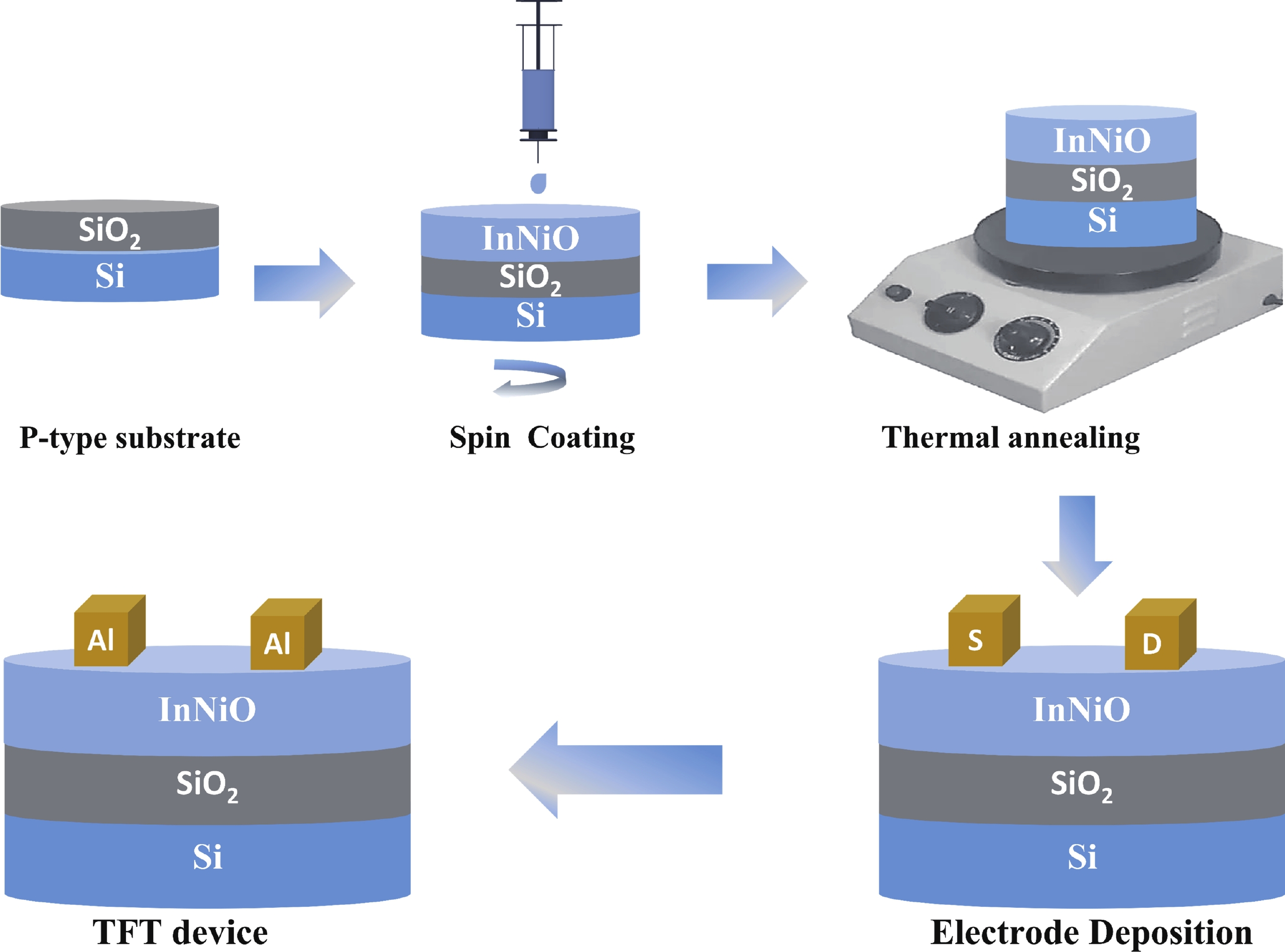
Fig. 1.
(Color online) A detailed illustration of the step-by-step fabrication process for a thin-film transistor device based on NiInO.
ARTICLES
Fakhari Alam1, 2, §, Sara Ajmal1, 3, , Muhammad Asim Shahzad5, §, Ghulam Dastgeer4, §, Aamir Rasheed1, 3, and Gang He1
Corresponding author: Sara Ajmal, sara786@ulsan.ac.kr; Aamir Rasheed, aamir786@ulsan.ac.kr
Abstract: Doping in thin-film transistors (TFTs) plays a crucial role in tailoring material properties to enhance device performance, making them essential for advanced electronic applications. This study explores the synthesis and characterization of TFTs fabricated using nickel (Ni)-doped indium oxide (In2O3) via a wet-chemical approach. The presented work investigates the effect of "Ni" incorporation in In2O3 on the structural and electrical transport properties of In2O3, revealing that higher "Ni" content decreases the oxygen vacancies, leading to a reduction in leakage current and a forward shift in threshold potential (Vth). Experimental findings reveal that NiInO-based TFTs (with Ni = 0.5%) showcase enhanced electrical performance, achieving mobility of 7.54 cm2/(V∙s), an impressive ON/OFF current ratio of ~107, a Vth of 6.26 V, reduced interfacial trap states (Dit) of 8.23 × 1012 cm−2 and enhanced biased stress stability. The efficacy of "Ni" incorporation is attributed to the upgraded Lewis acidity, stable Ni−O bond strength, and small ionic radius of Ni. Negative bias illumination stability (NBIS) measurements further indicate that device stability diminishes with shorter light wavelengths, likely due to the activation of oxygen vacancies. These findings validate the solution-processed techniques' potential for future large-scale, low-cost, energy-efficient, and high-performance electronics.
Keywords: thin-film transistors, Ni-doped In2O3, solution processing, bias illumination stability
| [1] |
Nomura K, Ohta H, Takagi A, et al. Room-temperature fabrication of transparent flexible thin-film transistors using amorphous oxide semiconductor. Nature, 2004, 432(7016): 488 doi: 10.1038/nature03090
|
| [2] |
Ahn B D, Park J S, Chung K B. Facile fabrication of high-performance InGaZnO thin film transistor using hydrogen ion irradiation at room temperature. Appl Phys Lett, 2014, 105(16): 163505 doi: 10.1063/1.4899144
|
| [3] |
Yabuta, H, Sano M, Abe K, et al. High-mobility thin-film transistor with amorphous InGaZnO4 channel fabricated by room temperature Rf-magnetron sputtering. Appl Phys Lett, 2006, 89(11): 112123 doi: 10.1063/1.2353811
|
| [4] |
Zhang X N, Wang B H, Haung W, et al. Synergistic boron doping of semiconductor and dielectric layers for high-performance metal oxide transistors: Interplay of experiment and theory. J Am Chem Soc, 2018, 140(39): 12501 doi: 10.1021/jacs.8b06395
|
| [5] |
Li H U, Jackson T N. Oxide semiconductor thin film transistors on thin solution-cast flexible substrates. IEEE Electron Device Lett, 2015, 36(1): 35 doi: 10.1109/LED.2014.2371011
|
| [6] |
Kim M G, Kanatzids M G, Facchetti A, et al. Low-temperature fabrication of high-performance metal oxide thin-film electronics via combustion processing. Nat Mater, 2011, 10(5): 382 doi: 10.1038/nmat3011
|
| [7] |
Seo S J, Choi C G, Hwang Y H, et al. Transparent amorphous oxide thin film transistors fabricated by solution coating process. Symposium Digest Tech Papers, 2008, 39(1): 1245 doi: 10.1889/1.3069365
|
| [8] |
Jeong S, Ha Y G, Moon J. Role of gallium doping in dramatically lowering amorphous-oxide processing temperatures for solution-derived indium zinc oxide thin-film transistors. Adv Mater, 2010, 22(12): 1346 doi: 10.1002/adma.200902450
|
| [9] |
Kamiya T, Nomura K, Hosono H. Present status of amorphous In−Ga−Zn−O thin-film transistors. Sci Technol Adv Mater, 2010, 11(4): 044305 doi: 10.1088/1468-6996/11/4/044305
|
| [10] |
Xu W Y, Hu L Y, Zhao C, et al. Low temperature solution-processed IGZO thin-film transistors. Appl Surf Sci, 2018, 455: 554 doi: 10.1016/j.apsusc.2018.06.005
|
| [11] |
Mitoma N, Aikawa S, Ou-Yang W, et al. Dopant selection for control of charge carrier density and mobility in amorphous indium oxide thin-film transistors: Comparison between Si-and W-dopants. Appl Phys Lett., 2015, 106(4): 042106 doi: 10.1063/1.4907285
|
| [12] |
Lin Z G, Lan L F, Sun S, et al. Solution-processed high-mobility neodymium-substituted indium oxide thin-film transistors formed by facile patterning based on aqueous precursors. Appl Phys Lett, 2017, 110(13): 133502 doi: 10.1063/1.4979318
|
| [13] |
Aikawa, S, Mitoma N. Kizu T, et al. Suppression of excess oxygen for environmentally stable amorphous In-Si-O thin-film transistors. Appl Phys Lett, 2015, 106(19): 192103 doi: 10.1063/1.4921054
|
| [14] |
Gandla S, Gollu S R, Sharma R. Dual role of boron in improving electrical performance and device stability of low temperature solution processed ZnO thin film transistors. Appl Phys Lett, 2015, 107(15): 152102 doi: 10.1063/1.4933304
|
| [15] |
Lee S H, Kim T, Lee J H, et al. Solution-processed gadolinium doped indium-oxide thin-film transistors with oxide passivation. Appl Phys Lett, 2017, 110(12): 122102 doi: 10.1063/1.4978932
|
| [16] |
Everaerts K, Zeng L, Hennek J W, et al. Printed indium gallium zinc oxide transistors. Self-assembled nanodielectric effects on low-temperature combustion growth and carrier mobility. ACS appl Mater Interfaces, 2013, 5(22): 11884 doi: 10.1021/am403585n
|
| [17] |
Song W, Lan L F, Li M L, et al. High-performance thin-film transistors with solution-processed ScInO channel layer based on environmental friendly precursor. J Phys D: Appl Phys, 2017, 50(38): 385108. doi: 10.1088/1361-6463/aa83ee
|
| [18] |
Zhao C Y, Li J, Zhong D Y, et al. Effect of La addition on the electrical characteristics and stability of solution-processed LaInO thin-film transistors with high-k ZrO2 gate insulator. IEEE Electron Devices, 2018, 65(2): 526 doi: 10.1109/TED.2017.2781725
|
| [19] |
Parthiban S, Kwon J Y. Role of dopants as a carrier suppressor and strong oxygen binder in amorphous indium-oxide-based field effect transistor. J Mater Res, 2014, 29(15): 1585 doi: 10.1557/jmr.2014.187
|
| [20] |
Kim T, Jang B, Bae J H, et al. Improvement in the performance of sol−gel processed In2O3 thin-film transistor depending on Sb dopant concentration. IEEE Electron Device Lett, 2017, 38(8): 1027 doi: 10.1109/LED.2017.2715374
|
| [21] |
Kim Y G, Kim T, Avi C, et al. Stable and high-performance indium oxide thin-film transistor by Ga doping. IEEE Trans Electron Devices, 2016, 63(3): 1078 doi: 10.1109/TED.2016.2518703
|
| [22] |
Ting C C, Fan H Y, Tsai M K, et al. Improvement of electrical characteristics in the solution-processed nanocrystalline indium oxide thin-film transistors depending on yttrium doping concentration. Phys Status Solid A, 2014, 211(4): 800 doi: 10.1002/pssa.201330164
|
| [23] |
Zhao Y H, Li, J, Zhong D Y, et al. Mg doping to simultaneously improve the electrical performance and stability of MgInO thin-film transistors. IEEE Trans Electron Devices, 2017, 64(5): 2216 doi: 10.1109/TED.2017.2678544
|
| [24] |
Zhou Y H, Li J, Zhong D Y, et al. Enhanced stability of Sr-doped aqueous In2O3 thin-film transistors under bias/illumination/thermal stress. IEEE Trans Electron Devices, 2019, 66(3): 1308 doi: 10.1109/TED.2019.2893479
|
| [25] |
Manoharan C, Jothibas M, Dhanapandian S, et al. Role of titanium doping on indium oxide thin films using spray pyrolysis techniques. International Conference on Advanced Nanomaterials & Emerging Engineering Technologies, 2013: 335 doi: 10.1109/ICANMEET.2013.6609310
|
| [26] |
Das S C, Green R J, Podder J, et al. Band gap tuning in ZnO through Ni doping via spray pyrolysis. J Phys Chem C, 2013, 117(24): 12745 doi: 10.1021/jp3126329
|
| [27] |
Shannon R D. Revised effective ionic radii and systematic studies of interatomic distances in halides and chalcogenides. Acta Cryst A, Section A 1976, 32(5): 751 doi: 10.1107/S0567739476001551
|
| [28] |
Abliz A, Xu L, Wan D, et al. Effects of yttrium doping on the electrical performances and stability of ZnO thin-film transistors. Appl Surf Sci, 2019, 475: 565 doi: 10.1016/j.apsusc.2018.12.236
|
| [29] |
Cui J B, Gibson U J. Enhanced nucleation, growth rate, and dopant incorporation in ZnO nanowires. J Phys Chem B, 2005, 109(46): 22074 doi: 10.1021/jp054160e
|
| [30] |
Liu X F, Yu R H. Mediation of room temperature ferromagnetism in Co-doped SnO2 nanocrystalline films by structural defects. J Appl Phys, 2007, 102(8): 083917 doi: 10.1063/1.2801375
|
| [31] |
Quilty J W, Shibata A, Son J Y, et al. Signature of carrier-induced ferromagnetism in Ti1−xCoxO2−δ. exchange interaction between high-spin Co2+ and the Ti 3d conduction band. Phys Rev Lett, 2006, 96(2): 027202 doi: 10.1103/PhysRevLett.96.027202
|
| [32] |
Yang J W, Ren J H, Lin D, et al. Amorphous nickel incorporated tin oxide thin film transistors. J Phys D: Appl Phys, 2017, 50(35): 355103 doi: 10.1088/1361-6463/aa7c53
|
| [33] |
Wang W H, He G, Wang L N, et al. Solution-driven HfLaOx-based gate dielectrics for thin film transistors and unipolar inverters. IEEE Trans Electron Devices, 2021, 68(9): 4437 doi: 10.1109/TED.2021.3095039
|
| [34] |
Liu A, Liu G X, Zhu H H, et al. Eco-friendly, solution-processed In-WO thin films and their applications in low-voltage, high-performance transistors. J Mater Chem C, 2016, 4(20): 4478 doi: 10.1039/C6TC00474A
|
| [35] |
Ko J, Kim J, Park S Y, et al. Solution-processed amorphous hafnium-lanthanum oxide gate insulator for oxide thin-film transistors. J Mater Chem C, 2014, 2(6): 1050 doi: 10.1039/C3TC31727G
|
| [36] |
Song K, Yang W, Jung Y. et al. A solution-processed yttrium oxide gate insulator for high-performance all-solution-processed fully transparent thin film transistors. J Mater Chem, 2012, 22(39): 21265 doi: 10.1039/c2jm34162j
|
| [37] |
Cuenya B R. Metal oxide nanoparticles for solar energy conversion. Phys Chem Chem Phys, 2013, 15(36): 16517 doi: 10.2174/1877944111202020124
|
| [38] |
Shin D M, Lee S H, Kang Y S, et al. Optical and structural properties of Ni-doped In2O3 films. J Appl Phys, 2011, 109(11): 113508 doi: 10.1063/1.3592214
|
| [39] |
Wang J W, Shi Y. Room temperature ferromagnetism studies in Fe ion implanted indium oxide films. Mater Sci Semicond Process, 2014, 27: 314 doi: 10.1016/j.mssp.2014.07.011
|
| [40] |
Li K Y, Xue D F. Estimation of electronegativity values of elements in different valence states. J Phys Chem A, 2006, 110(39): 11332 doi: 10.1021/jp062886k
|
| [41] |
Seo J S, Jeon J H, Hwang Y H, et al. Solution-processed flexible fluorine-doped indium zinc oxide thin-film transistors fabricated on plastic film at low temperature. Sci Rep, 2013, 3: 208 doi: 10.1038/srep02085
|
| [42] |
Lide D R. CRC handbook of chemistry and physics. CRC Press, 2004: 85
|
| [43] |
Conley J F. Instabilities in amorphous oxide semiconductor thin-film transistors. IEEE Trans Device Mater Reliab, 2010, 10(4): 460 doi: 10.1109/TDMR.2010.2069561
|
| [44] |
Jeong J K, Yang H W, Jeong J H, et al. Origin of threshold voltage instability in indium-gallium-zinc oxide thin film transistors. Appl Phys Lett, 2008, 93(12): 123508 doi: 10.1063/1.2990657
|
| [45] |
Liu P T, Chou Y T, Teng L F. Environment-dependent metastability of passivation-free indium zinc oxide thin film transistor after gate bias stress. Appl Phys Lett, 2009, 95(23): 233504 doi: 10.1063/1.3272016
|
| [46] |
Liu L C, Chen J S, Jeng J S. Role of oxygen vacancies on the bias illumination stress stability of solution-processed zinc tin oxide thin film transistors. Appl Phys Lett, 2014, 105(2): 023509 doi: 10.1063/1.4890579
|
| [47] |
Huang C X, Li J, Fu Y Z, et al. Suppression in the negative bias illumination instability of ZnSnO thin-film transistors using hafnium doping by dual-target magnetron Cosputtering system. IEEE Trans Electron Devices, 2016, 63(9): 3552 doi: 10.1109/TED.2016.2589240
|
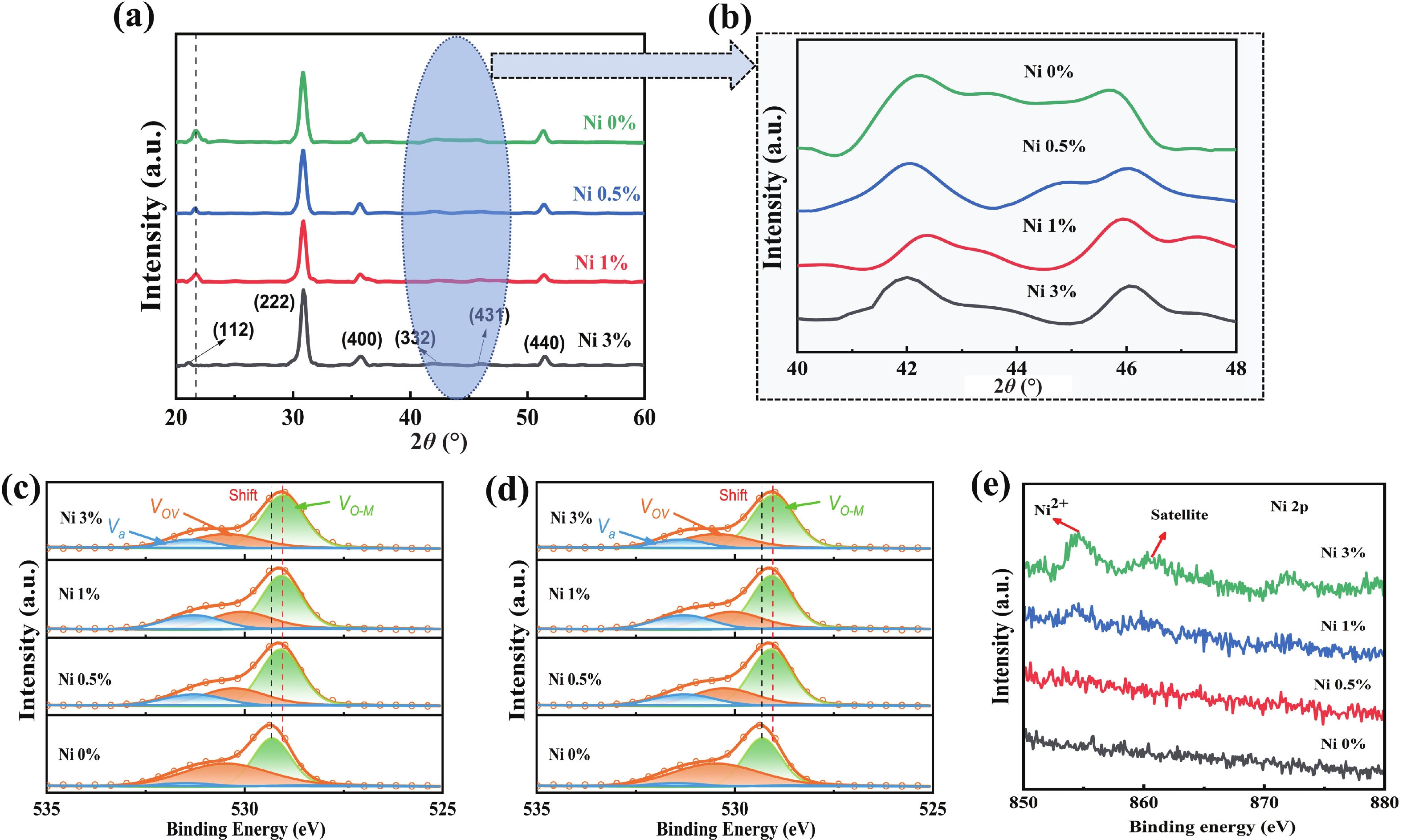
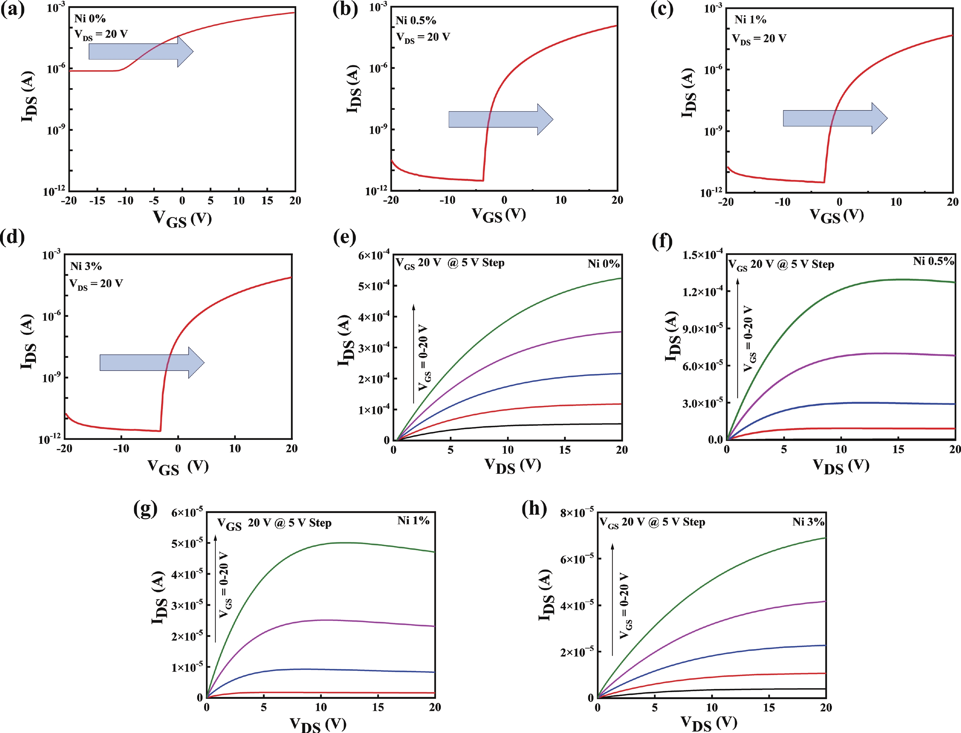
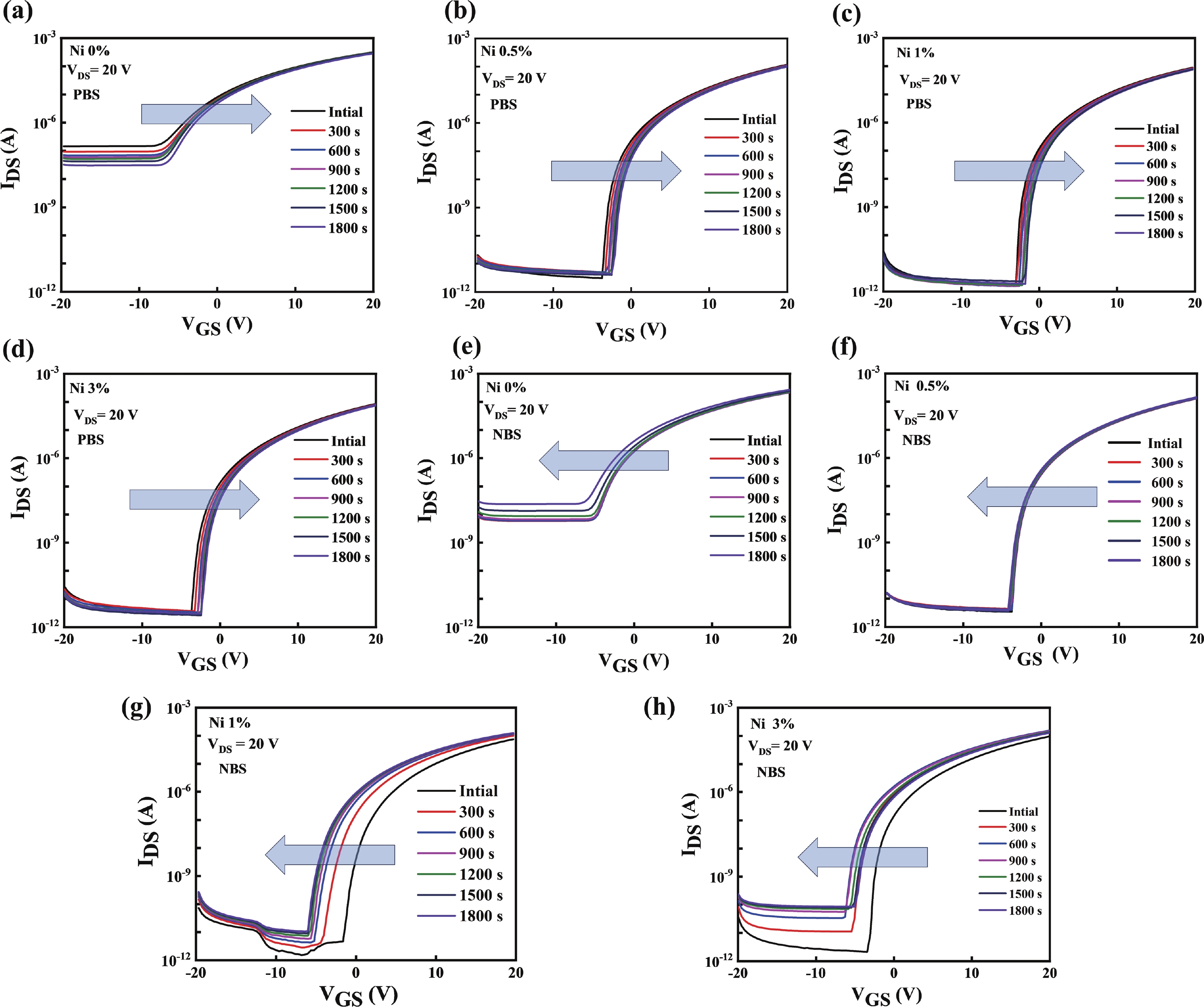
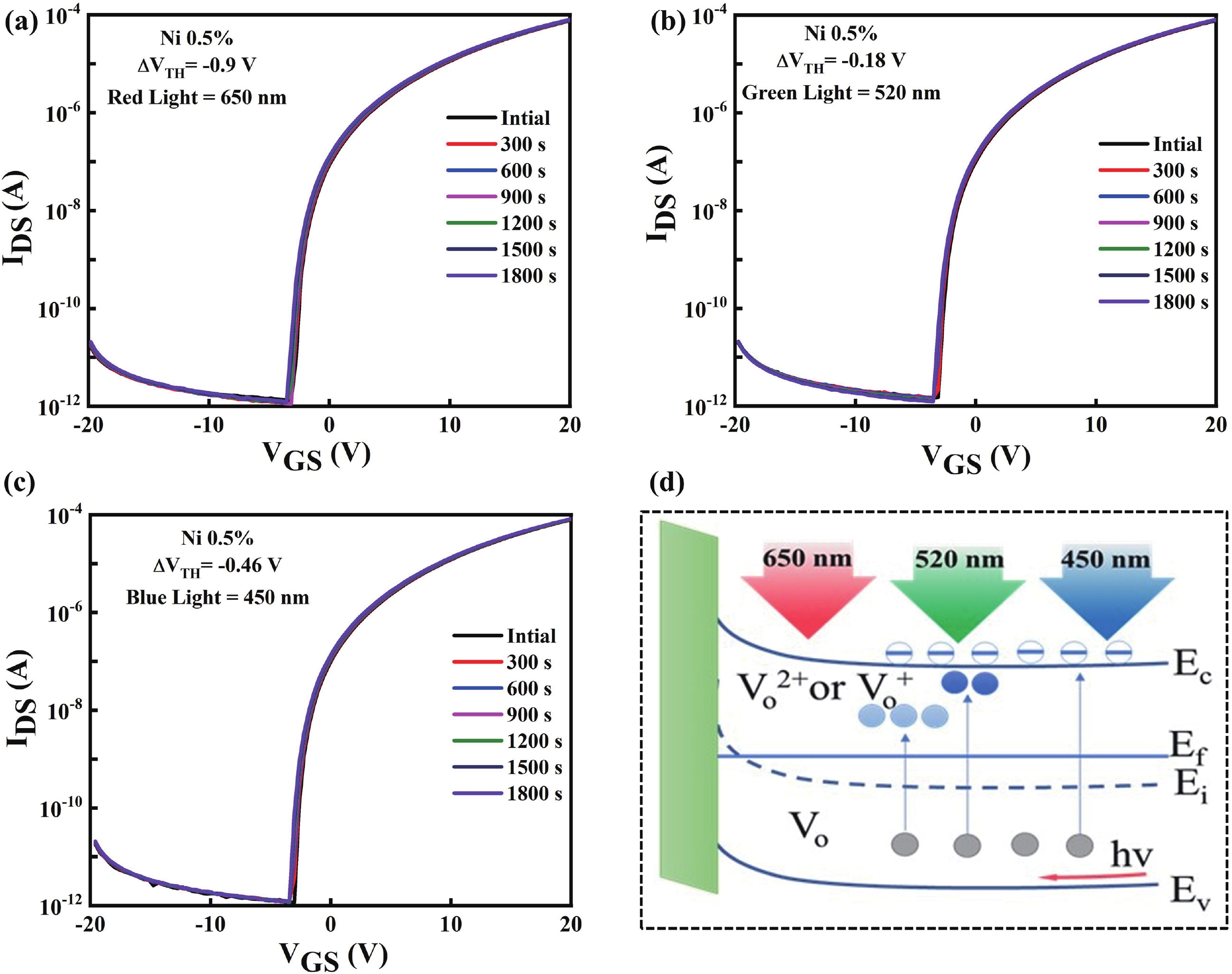
Table 1. Positions, areas, and Oⅱ/Ototal ratios of XPS O1s peak for the NiInO films with 0, 0.5%, 1%, or 3% Ni concentrations.
| Oⅱ/Ototal (%) | Area and position of peak | For given Ni concentration (%) | |||
| 0 | 0.5 | 1 | 3 | ||
| Oi | Position (eV) | 529.31 | 529.12 | 529.08 | 529.02 |
| Area (m2) | 51764.96 | 85020.61 | 87038.67 | 101600.41 | |
| Oⅱ | Position (eV) | 530.51 | 530.34 | 530.09 | 530.48 |
| Area (m2) | 56782.71 | 41373.26 | 43726.97 | 42127.65 | |
| Oⅲ | Position (eV) | 531.55 | 531.28 | 531.29 | 531.44 |
| Area (m2) | 5826.68 | 26830.57 | 34614.23 | 19581.08 | |
| Oⅱ/Ototal | 49.65 | 27.01 | 26.4 | 25.7 | |
 DownLoad: CSV
Table 2. Electrical properties of NiInO TFTs under various concentrations of the Ni doping.
| Ni-doping ratio (%) | μ (cm2/(V∙s)) | ION/IOFF | Vth (V) | SS (V/dec) | Dit (cm−2) |
| 0 | 13.24 | 1.5 × 10² | −8.80 | 4.87 | 3.87 × 10¹³ |
| 0.5 | 7.54 | 3.06 × 10⁷ | 5.05 | 3.54 | 8.23 × 10¹² |
| 1 | 3.75 | 4.10 × 10⁶ | 7.66 | 7.63 | 5.4 × 10¹² |
| 3 | 2.10 | 7.21 × 10⁶ | 9.46 | 5.95 | 9.05 × 10¹² |
DownLoad: CSV
Table 3. Summary of the latest development in In−X−O TFTs by solution processing.
| Channel | Solvent | Temp | Die-electric | Mobility (cm2/(V∙s)) | ION/IOFF | Ref |
| In−Y−O | HAC/2ME | 500 | SiO2 | 0.95 | 105 | [22] |
| In−Sc−O | DI water | 300 | Al2O3: Nd | 6.4 | 107 | [17] |
| In−Sb−O | Ethanol | 500 | SiO2 | 1.6 | 104 | [20] |
| In−B−O | 2-ME | 300 | SiO2 | 7.3 | 107 | [4] |
| In−Sr−O | DI water | 300 | Al2O3 | 5.4 | 105 | [24] |
| In−Ni−O | 2-ME | 330 | SiO2 | 7.5 | 107 | This study |
DownLoad: CSV
| [1] |
Nomura K, Ohta H, Takagi A, et al. Room-temperature fabrication of transparent flexible thin-film transistors using amorphous oxide semiconductor. Nature, 2004, 432(7016): 488 doi: 10.1038/nature03090
|
| [2] |
Ahn B D, Park J S, Chung K B. Facile fabrication of high-performance InGaZnO thin film transistor using hydrogen ion irradiation at room temperature. Appl Phys Lett, 2014, 105(16): 163505 doi: 10.1063/1.4899144
|
| [3] |
Yabuta, H, Sano M, Abe K, et al. High-mobility thin-film transistor with amorphous InGaZnO4 channel fabricated by room temperature Rf-magnetron sputtering. Appl Phys Lett, 2006, 89(11): 112123 doi: 10.1063/1.2353811
|
| [4] |
Zhang X N, Wang B H, Haung W, et al. Synergistic boron doping of semiconductor and dielectric layers for high-performance metal oxide transistors: Interplay of experiment and theory. J Am Chem Soc, 2018, 140(39): 12501 doi: 10.1021/jacs.8b06395
|
| [5] |
Li H U, Jackson T N. Oxide semiconductor thin film transistors on thin solution-cast flexible substrates. IEEE Electron Device Lett, 2015, 36(1): 35 doi: 10.1109/LED.2014.2371011
|
| [6] |
Kim M G, Kanatzids M G, Facchetti A, et al. Low-temperature fabrication of high-performance metal oxide thin-film electronics via combustion processing. Nat Mater, 2011, 10(5): 382 doi: 10.1038/nmat3011
|
| [7] |
Seo S J, Choi C G, Hwang Y H, et al. Transparent amorphous oxide thin film transistors fabricated by solution coating process. Symposium Digest Tech Papers, 2008, 39(1): 1245 doi: 10.1889/1.3069365
|
| [8] |
Jeong S, Ha Y G, Moon J. Role of gallium doping in dramatically lowering amorphous-oxide processing temperatures for solution-derived indium zinc oxide thin-film transistors. Adv Mater, 2010, 22(12): 1346 doi: 10.1002/adma.200902450
|
| [9] |
Kamiya T, Nomura K, Hosono H. Present status of amorphous In−Ga−Zn−O thin-film transistors. Sci Technol Adv Mater, 2010, 11(4): 044305 doi: 10.1088/1468-6996/11/4/044305
|
| [10] |
Xu W Y, Hu L Y, Zhao C, et al. Low temperature solution-processed IGZO thin-film transistors. Appl Surf Sci, 2018, 455: 554 doi: 10.1016/j.apsusc.2018.06.005
|
| [11] |
Mitoma N, Aikawa S, Ou-Yang W, et al. Dopant selection for control of charge carrier density and mobility in amorphous indium oxide thin-film transistors: Comparison between Si-and W-dopants. Appl Phys Lett., 2015, 106(4): 042106 doi: 10.1063/1.4907285
|
| [12] |
Lin Z G, Lan L F, Sun S, et al. Solution-processed high-mobility neodymium-substituted indium oxide thin-film transistors formed by facile patterning based on aqueous precursors. Appl Phys Lett, 2017, 110(13): 133502 doi: 10.1063/1.4979318
|
| [13] |
Aikawa, S, Mitoma N. Kizu T, et al. Suppression of excess oxygen for environmentally stable amorphous In-Si-O thin-film transistors. Appl Phys Lett, 2015, 106(19): 192103 doi: 10.1063/1.4921054
|
| [14] |
Gandla S, Gollu S R, Sharma R. Dual role of boron in improving electrical performance and device stability of low temperature solution processed ZnO thin film transistors. Appl Phys Lett, 2015, 107(15): 152102 doi: 10.1063/1.4933304
|
| [15] |
Lee S H, Kim T, Lee J H, et al. Solution-processed gadolinium doped indium-oxide thin-film transistors with oxide passivation. Appl Phys Lett, 2017, 110(12): 122102 doi: 10.1063/1.4978932
|
| [16] |
Everaerts K, Zeng L, Hennek J W, et al. Printed indium gallium zinc oxide transistors. Self-assembled nanodielectric effects on low-temperature combustion growth and carrier mobility. ACS appl Mater Interfaces, 2013, 5(22): 11884 doi: 10.1021/am403585n
|
| [17] |
Song W, Lan L F, Li M L, et al. High-performance thin-film transistors with solution-processed ScInO channel layer based on environmental friendly precursor. J Phys D: Appl Phys, 2017, 50(38): 385108. doi: 10.1088/1361-6463/aa83ee
|
| [18] |
Zhao C Y, Li J, Zhong D Y, et al. Effect of La addition on the electrical characteristics and stability of solution-processed LaInO thin-film transistors with high-k ZrO2 gate insulator. IEEE Electron Devices, 2018, 65(2): 526 doi: 10.1109/TED.2017.2781725
|
| [19] |
Parthiban S, Kwon J Y. Role of dopants as a carrier suppressor and strong oxygen binder in amorphous indium-oxide-based field effect transistor. J Mater Res, 2014, 29(15): 1585 doi: 10.1557/jmr.2014.187
|
| [20] |
Kim T, Jang B, Bae J H, et al. Improvement in the performance of sol−gel processed In2O3 thin-film transistor depending on Sb dopant concentration. IEEE Electron Device Lett, 2017, 38(8): 1027 doi: 10.1109/LED.2017.2715374
|
| [21] |
Kim Y G, Kim T, Avi C, et al. Stable and high-performance indium oxide thin-film transistor by Ga doping. IEEE Trans Electron Devices, 2016, 63(3): 1078 doi: 10.1109/TED.2016.2518703
|
| [22] |
Ting C C, Fan H Y, Tsai M K, et al. Improvement of electrical characteristics in the solution-processed nanocrystalline indium oxide thin-film transistors depending on yttrium doping concentration. Phys Status Solid A, 2014, 211(4): 800 doi: 10.1002/pssa.201330164
|
| [23] |
Zhao Y H, Li, J, Zhong D Y, et al. Mg doping to simultaneously improve the electrical performance and stability of MgInO thin-film transistors. IEEE Trans Electron Devices, 2017, 64(5): 2216 doi: 10.1109/TED.2017.2678544
|
| [24] |
Zhou Y H, Li J, Zhong D Y, et al. Enhanced stability of Sr-doped aqueous In2O3 thin-film transistors under bias/illumination/thermal stress. IEEE Trans Electron Devices, 2019, 66(3): 1308 doi: 10.1109/TED.2019.2893479
|
| [25] |
Manoharan C, Jothibas M, Dhanapandian S, et al. Role of titanium doping on indium oxide thin films using spray pyrolysis techniques. International Conference on Advanced Nanomaterials & Emerging Engineering Technologies, 2013: 335 doi: 10.1109/ICANMEET.2013.6609310
|
| [26] |
Das S C, Green R J, Podder J, et al. Band gap tuning in ZnO through Ni doping via spray pyrolysis. J Phys Chem C, 2013, 117(24): 12745 doi: 10.1021/jp3126329
|
| [27] |
Shannon R D. Revised effective ionic radii and systematic studies of interatomic distances in halides and chalcogenides. Acta Cryst A, Section A 1976, 32(5): 751 doi: 10.1107/S0567739476001551
|
| [28] |
Abliz A, Xu L, Wan D, et al. Effects of yttrium doping on the electrical performances and stability of ZnO thin-film transistors. Appl Surf Sci, 2019, 475: 565 doi: 10.1016/j.apsusc.2018.12.236
|
| [29] |
Cui J B, Gibson U J. Enhanced nucleation, growth rate, and dopant incorporation in ZnO nanowires. J Phys Chem B, 2005, 109(46): 22074 doi: 10.1021/jp054160e
|
| [30] |
Liu X F, Yu R H. Mediation of room temperature ferromagnetism in Co-doped SnO2 nanocrystalline films by structural defects. J Appl Phys, 2007, 102(8): 083917 doi: 10.1063/1.2801375
|
| [31] |
Quilty J W, Shibata A, Son J Y, et al. Signature of carrier-induced ferromagnetism in Ti1−xCoxO2−δ. exchange interaction between high-spin Co2+ and the Ti 3d conduction band. Phys Rev Lett, 2006, 96(2): 027202 doi: 10.1103/PhysRevLett.96.027202
|
| [32] |
Yang J W, Ren J H, Lin D, et al. Amorphous nickel incorporated tin oxide thin film transistors. J Phys D: Appl Phys, 2017, 50(35): 355103 doi: 10.1088/1361-6463/aa7c53
|
| [33] |
Wang W H, He G, Wang L N, et al. Solution-driven HfLaOx-based gate dielectrics for thin film transistors and unipolar inverters. IEEE Trans Electron Devices, 2021, 68(9): 4437 doi: 10.1109/TED.2021.3095039
|
| [34] |
Liu A, Liu G X, Zhu H H, et al. Eco-friendly, solution-processed In-WO thin films and their applications in low-voltage, high-performance transistors. J Mater Chem C, 2016, 4(20): 4478 doi: 10.1039/C6TC00474A
|
| [35] |
Ko J, Kim J, Park S Y, et al. Solution-processed amorphous hafnium-lanthanum oxide gate insulator for oxide thin-film transistors. J Mater Chem C, 2014, 2(6): 1050 doi: 10.1039/C3TC31727G
|
| [36] |
Song K, Yang W, Jung Y. et al. A solution-processed yttrium oxide gate insulator for high-performance all-solution-processed fully transparent thin film transistors. J Mater Chem, 2012, 22(39): 21265 doi: 10.1039/c2jm34162j
|
| [37] |
Cuenya B R. Metal oxide nanoparticles for solar energy conversion. Phys Chem Chem Phys, 2013, 15(36): 16517 doi: 10.2174/1877944111202020124
|
| [38] |
Shin D M, Lee S H, Kang Y S, et al. Optical and structural properties of Ni-doped In2O3 films. J Appl Phys, 2011, 109(11): 113508 doi: 10.1063/1.3592214
|
| [39] |
Wang J W, Shi Y. Room temperature ferromagnetism studies in Fe ion implanted indium oxide films. Mater Sci Semicond Process, 2014, 27: 314 doi: 10.1016/j.mssp.2014.07.011
|
| [40] |
Li K Y, Xue D F. Estimation of electronegativity values of elements in different valence states. J Phys Chem A, 2006, 110(39): 11332 doi: 10.1021/jp062886k
|
| [41] |
Seo J S, Jeon J H, Hwang Y H, et al. Solution-processed flexible fluorine-doped indium zinc oxide thin-film transistors fabricated on plastic film at low temperature. Sci Rep, 2013, 3: 208 doi: 10.1038/srep02085
|
| [42] |
Lide D R. CRC handbook of chemistry and physics. CRC Press, 2004: 85
|
| [43] |
Conley J F. Instabilities in amorphous oxide semiconductor thin-film transistors. IEEE Trans Device Mater Reliab, 2010, 10(4): 460 doi: 10.1109/TDMR.2010.2069561
|
| [44] |
Jeong J K, Yang H W, Jeong J H, et al. Origin of threshold voltage instability in indium-gallium-zinc oxide thin film transistors. Appl Phys Lett, 2008, 93(12): 123508 doi: 10.1063/1.2990657
|
| [45] |
Liu P T, Chou Y T, Teng L F. Environment-dependent metastability of passivation-free indium zinc oxide thin film transistor after gate bias stress. Appl Phys Lett, 2009, 95(23): 233504 doi: 10.1063/1.3272016
|
| [46] |
Liu L C, Chen J S, Jeng J S. Role of oxygen vacancies on the bias illumination stress stability of solution-processed zinc tin oxide thin film transistors. Appl Phys Lett, 2014, 105(2): 023509 doi: 10.1063/1.4890579
|
| [47] |
Huang C X, Li J, Fu Y Z, et al. Suppression in the negative bias illumination instability of ZnSnO thin-film transistors using hafnium doping by dual-target magnetron Cosputtering system. IEEE Trans Electron Devices, 2016, 63(9): 3552 doi: 10.1109/TED.2016.2589240
|


Article views: 1283 Times PDF downloads: 163 Times Cited by: 0 Times
Received: 19 March 2025 Revised: 12 August 2025 Online: Accepted Manuscript: 18 September 2025Uncorrected proof: 23 September 2025Published: 15 February 2026
| Citation: |
Fakhari Alam, Sara Ajmal, Muhammad Asim Shahzad, Ghulam Dastgeer, Aamir Rasheed, Gang He. Tailoring oxygen vacancies in Ni-doped In2O3 for improved thin-film transistor stability and performance via solution processing[J]. Journal of Semiconductors, 2026, 47(2): 022304. doi: 10.1088/1674-4926/25030033
****
F Alam, S Ajmal, M A Shahzad, G Dastgeer, A Rasheed, and G He, Tailoring oxygen vacancies in Ni-doped In2O3 for improved thin-film transistor stability and performance via solution processing[J]. J. Semicond., 2026, 47(2): 022304 doi: 10.1088/1674-4926/25030033

|
 Fakhari Alam got his Ph.D. from Anhui University, China, in 2023. He is currently pursuing post-doctoral research at the same institution. His primary research focus is on Oxide Thin Film Transistors (TFTs), a key technology in the development of next-generation electronic displays and devices
 Muhammad Asim Shahzad is a dedicated researcher in nanomaterials, specializing in their synthesis, characterization, and applications in energy storage devices. He serves as a faculty member in the Department of Physics, University of Sahiwal, Pakistan, with research focused on dielectric materials, supercapacitors, and their integration into next-generation electronic and energy applications
 Aamir Rasheed is a distinguished researcher specializing in the synthesis of functional two-dimensional (2D) materials and their heterostructures with metal oxides, with a particular focus on applications in energy harvesting and storage devices. He completed his Ph.D. from Sungkyunkwan University, South Korea, where he developed a solid foundation in advanced material science and nanotechnology. Currently, Dr. Rasheed is a faculty member at University of Ulsan, South Korea where he continues to advance his research in the field of nanogenerators and supercapacitors. His research is instrumental in paving the way for future technological advancements in renewable energy and portable power sources
| [1] |
Nomura K, Ohta H, Takagi A, et al. Room-temperature fabrication of transparent flexible thin-film transistors using amorphous oxide semiconductor. Nature, 2004, 432(7016): 488 doi: 10.1038/nature03090
|
| [2] |
Ahn B D, Park J S, Chung K B. Facile fabrication of high-performance InGaZnO thin film transistor using hydrogen ion irradiation at room temperature. Appl Phys Lett, 2014, 105(16): 163505 doi: 10.1063/1.4899144
|
| [3] |
Yabuta, H, Sano M, Abe K, et al. High-mobility thin-film transistor with amorphous InGaZnO4 channel fabricated by room temperature Rf-magnetron sputtering. Appl Phys Lett, 2006, 89(11): 112123 doi: 10.1063/1.2353811
|
| [4] |
Zhang X N, Wang B H, Haung W, et al. Synergistic boron doping of semiconductor and dielectric layers for high-performance metal oxide transistors: Interplay of experiment and theory. J Am Chem Soc, 2018, 140(39): 12501 doi: 10.1021/jacs.8b06395
|
| [5] |
Li H U, Jackson T N. Oxide semiconductor thin film transistors on thin solution-cast flexible substrates. IEEE Electron Device Lett, 2015, 36(1): 35 doi: 10.1109/LED.2014.2371011
|
| [6] |
Kim M G, Kanatzids M G, Facchetti A, et al. Low-temperature fabrication of high-performance metal oxide thin-film electronics via combustion processing. Nat Mater, 2011, 10(5): 382 doi: 10.1038/nmat3011
|
| [7] |
Seo S J, Choi C G, Hwang Y H, et al. Transparent amorphous oxide thin film transistors fabricated by solution coating process. Symposium Digest Tech Papers, 2008, 39(1): 1245 doi: 10.1889/1.3069365
|
| [8] |
Jeong S, Ha Y G, Moon J. Role of gallium doping in dramatically lowering amorphous-oxide processing temperatures for solution-derived indium zinc oxide thin-film transistors. Adv Mater, 2010, 22(12): 1346 doi: 10.1002/adma.200902450
|
| [9] |
Kamiya T, Nomura K, Hosono H. Present status of amorphous In−Ga−Zn−O thin-film transistors. Sci Technol Adv Mater, 2010, 11(4): 044305 doi: 10.1088/1468-6996/11/4/044305
|
| [10] |
Xu W Y, Hu L Y, Zhao C, et al. Low temperature solution-processed IGZO thin-film transistors. Appl Surf Sci, 2018, 455: 554 doi: 10.1016/j.apsusc.2018.06.005
|
| [11] |
Mitoma N, Aikawa S, Ou-Yang W, et al. Dopant selection for control of charge carrier density and mobility in amorphous indium oxide thin-film transistors: Comparison between Si-and W-dopants. Appl Phys Lett., 2015, 106(4): 042106 doi: 10.1063/1.4907285
|
| [12] |
Lin Z G, Lan L F, Sun S, et al. Solution-processed high-mobility neodymium-substituted indium oxide thin-film transistors formed by facile patterning based on aqueous precursors. Appl Phys Lett, 2017, 110(13): 133502 doi: 10.1063/1.4979318
|
| [13] |
Aikawa, S, Mitoma N. Kizu T, et al. Suppression of excess oxygen for environmentally stable amorphous In-Si-O thin-film transistors. Appl Phys Lett, 2015, 106(19): 192103 doi: 10.1063/1.4921054
|
| [14] |
Gandla S, Gollu S R, Sharma R. Dual role of boron in improving electrical performance and device stability of low temperature solution processed ZnO thin film transistors. Appl Phys Lett, 2015, 107(15): 152102 doi: 10.1063/1.4933304
|
| [15] |
Lee S H, Kim T, Lee J H, et al. Solution-processed gadolinium doped indium-oxide thin-film transistors with oxide passivation. Appl Phys Lett, 2017, 110(12): 122102 doi: 10.1063/1.4978932
|
| [16] |
Everaerts K, Zeng L, Hennek J W, et al. Printed indium gallium zinc oxide transistors. Self-assembled nanodielectric effects on low-temperature combustion growth and carrier mobility. ACS appl Mater Interfaces, 2013, 5(22): 11884 doi: 10.1021/am403585n
|
| [17] |
Song W, Lan L F, Li M L, et al. High-performance thin-film transistors with solution-processed ScInO channel layer based on environmental friendly precursor. J Phys D: Appl Phys, 2017, 50(38): 385108. doi: 10.1088/1361-6463/aa83ee
|
| [18] |
Zhao C Y, Li J, Zhong D Y, et al. Effect of La addition on the electrical characteristics and stability of solution-processed LaInO thin-film transistors with high-k ZrO2 gate insulator. IEEE Electron Devices, 2018, 65(2): 526 doi: 10.1109/TED.2017.2781725
|
| [19] |
Parthiban S, Kwon J Y. Role of dopants as a carrier suppressor and strong oxygen binder in amorphous indium-oxide-based field effect transistor. J Mater Res, 2014, 29(15): 1585 doi: 10.1557/jmr.2014.187
|
| [20] |
Kim T, Jang B, Bae J H, et al. Improvement in the performance of sol−gel processed In2O3 thin-film transistor depending on Sb dopant concentration. IEEE Electron Device Lett, 2017, 38(8): 1027 doi: 10.1109/LED.2017.2715374
|
| [21] |
Kim Y G, Kim T, Avi C, et al. Stable and high-performance indium oxide thin-film transistor by Ga doping. IEEE Trans Electron Devices, 2016, 63(3): 1078 doi: 10.1109/TED.2016.2518703
|
| [22] |
Ting C C, Fan H Y, Tsai M K, et al. Improvement of electrical characteristics in the solution-processed nanocrystalline indium oxide thin-film transistors depending on yttrium doping concentration. Phys Status Solid A, 2014, 211(4): 800 doi: 10.1002/pssa.201330164
|
| [23] |
Zhao Y H, Li, J, Zhong D Y, et al. Mg doping to simultaneously improve the electrical performance and stability of MgInO thin-film transistors. IEEE Trans Electron Devices, 2017, 64(5): 2216 doi: 10.1109/TED.2017.2678544
|
| [24] |
Zhou Y H, Li J, Zhong D Y, et al. Enhanced stability of Sr-doped aqueous In2O3 thin-film transistors under bias/illumination/thermal stress. IEEE Trans Electron Devices, 2019, 66(3): 1308 doi: 10.1109/TED.2019.2893479
|
| [25] |
Manoharan C, Jothibas M, Dhanapandian S, et al. Role of titanium doping on indium oxide thin films using spray pyrolysis techniques. International Conference on Advanced Nanomaterials & Emerging Engineering Technologies, 2013: 335 doi: 10.1109/ICANMEET.2013.6609310
|
| [26] |
Das S C, Green R J, Podder J, et al. Band gap tuning in ZnO through Ni doping via spray pyrolysis. J Phys Chem C, 2013, 117(24): 12745 doi: 10.1021/jp3126329
|
| [27] |
Shannon R D. Revised effective ionic radii and systematic studies of interatomic distances in halides and chalcogenides. Acta Cryst A, Section A 1976, 32(5): 751 doi: 10.1107/S0567739476001551
|
| [28] |
Abliz A, Xu L, Wan D, et al. Effects of yttrium doping on the electrical performances and stability of ZnO thin-film transistors. Appl Surf Sci, 2019, 475: 565 doi: 10.1016/j.apsusc.2018.12.236
|
| [29] |
Cui J B, Gibson U J. Enhanced nucleation, growth rate, and dopant incorporation in ZnO nanowires. J Phys Chem B, 2005, 109(46): 22074 doi: 10.1021/jp054160e
|
| [30] |
Liu X F, Yu R H. Mediation of room temperature ferromagnetism in Co-doped SnO2 nanocrystalline films by structural defects. J Appl Phys, 2007, 102(8): 083917 doi: 10.1063/1.2801375
|
| [31] |
Quilty J W, Shibata A, Son J Y, et al. Signature of carrier-induced ferromagnetism in Ti1−xCoxO2−δ. exchange interaction between high-spin Co2+ and the Ti 3d conduction band. Phys Rev Lett, 2006, 96(2): 027202 doi: 10.1103/PhysRevLett.96.027202
|
| [32] |
Yang J W, Ren J H, Lin D, et al. Amorphous nickel incorporated tin oxide thin film transistors. J Phys D: Appl Phys, 2017, 50(35): 355103 doi: 10.1088/1361-6463/aa7c53
|
| [33] |
Wang W H, He G, Wang L N, et al. Solution-driven HfLaOx-based gate dielectrics for thin film transistors and unipolar inverters. IEEE Trans Electron Devices, 2021, 68(9): 4437 doi: 10.1109/TED.2021.3095039
|
| [34] |
Liu A, Liu G X, Zhu H H, et al. Eco-friendly, solution-processed In-WO thin films and their applications in low-voltage, high-performance transistors. J Mater Chem C, 2016, 4(20): 4478 doi: 10.1039/C6TC00474A
|
| [35] |
Ko J, Kim J, Park S Y, et al. Solution-processed amorphous hafnium-lanthanum oxide gate insulator for oxide thin-film transistors. J Mater Chem C, 2014, 2(6): 1050 doi: 10.1039/C3TC31727G
|
| [36] |
Song K, Yang W, Jung Y. et al. A solution-processed yttrium oxide gate insulator for high-performance all-solution-processed fully transparent thin film transistors. J Mater Chem, 2012, 22(39): 21265 doi: 10.1039/c2jm34162j
|
| [37] |
Cuenya B R. Metal oxide nanoparticles for solar energy conversion. Phys Chem Chem Phys, 2013, 15(36): 16517 doi: 10.2174/1877944111202020124
|
| [38] |
Shin D M, Lee S H, Kang Y S, et al. Optical and structural properties of Ni-doped In2O3 films. J Appl Phys, 2011, 109(11): 113508 doi: 10.1063/1.3592214
|
| [39] |
Wang J W, Shi Y. Room temperature ferromagnetism studies in Fe ion implanted indium oxide films. Mater Sci Semicond Process, 2014, 27: 314 doi: 10.1016/j.mssp.2014.07.011
|
| [40] |
Li K Y, Xue D F. Estimation of electronegativity values of elements in different valence states. J Phys Chem A, 2006, 110(39): 11332 doi: 10.1021/jp062886k
|
| [41] |
Seo J S, Jeon J H, Hwang Y H, et al. Solution-processed flexible fluorine-doped indium zinc oxide thin-film transistors fabricated on plastic film at low temperature. Sci Rep, 2013, 3: 208 doi: 10.1038/srep02085
|
| [42] |
Lide D R. CRC handbook of chemistry and physics. CRC Press, 2004: 85
|
| [43] |
Conley J F. Instabilities in amorphous oxide semiconductor thin-film transistors. IEEE Trans Device Mater Reliab, 2010, 10(4): 460 doi: 10.1109/TDMR.2010.2069561
|
| [44] |
Jeong J K, Yang H W, Jeong J H, et al. Origin of threshold voltage instability in indium-gallium-zinc oxide thin film transistors. Appl Phys Lett, 2008, 93(12): 123508 doi: 10.1063/1.2990657
|
| [45] |
Liu P T, Chou Y T, Teng L F. Environment-dependent metastability of passivation-free indium zinc oxide thin film transistor after gate bias stress. Appl Phys Lett, 2009, 95(23): 233504 doi: 10.1063/1.3272016
|
| [46] |
Liu L C, Chen J S, Jeng J S. Role of oxygen vacancies on the bias illumination stress stability of solution-processed zinc tin oxide thin film transistors. Appl Phys Lett, 2014, 105(2): 023509 doi: 10.1063/1.4890579
|
| [47] |
Huang C X, Li J, Fu Y Z, et al. Suppression in the negative bias illumination instability of ZnSnO thin-film transistors using hafnium doping by dual-target magnetron Cosputtering system. IEEE Trans Electron Devices, 2016, 63(9): 3552 doi: 10.1109/TED.2016.2589240
|
 Supporting_Information.pdf
|

|

 WeChat ID
Journal of Semiconductors © 2017 All Rights Reserved 京ICP备05085259号-2


