J. Semicond. >  In Press

REVIEWS

AlScN: characteristics, micro/nano fabrication and multiple applications

Shihang Liu1, Jinfeng Gao1, Jiajie Pan1, 2, Lin Li1, Hanxiang Jia1, , Shuangzan Lu1, Maowei Zhang1, Bo Zhao1 and Jun Liu1,

+ Author Affiliations

 Corresponding author: Hanxiang Jia, jiahanxiang@jfslab.com.cn; Jun Liu, liujun@jfslab.com.cn

DOI: 10.1088/1674-4926/25060031CSTR: 10.1088/1674-4926/25060031

PDF

Turn off MathJax

Abstract: 
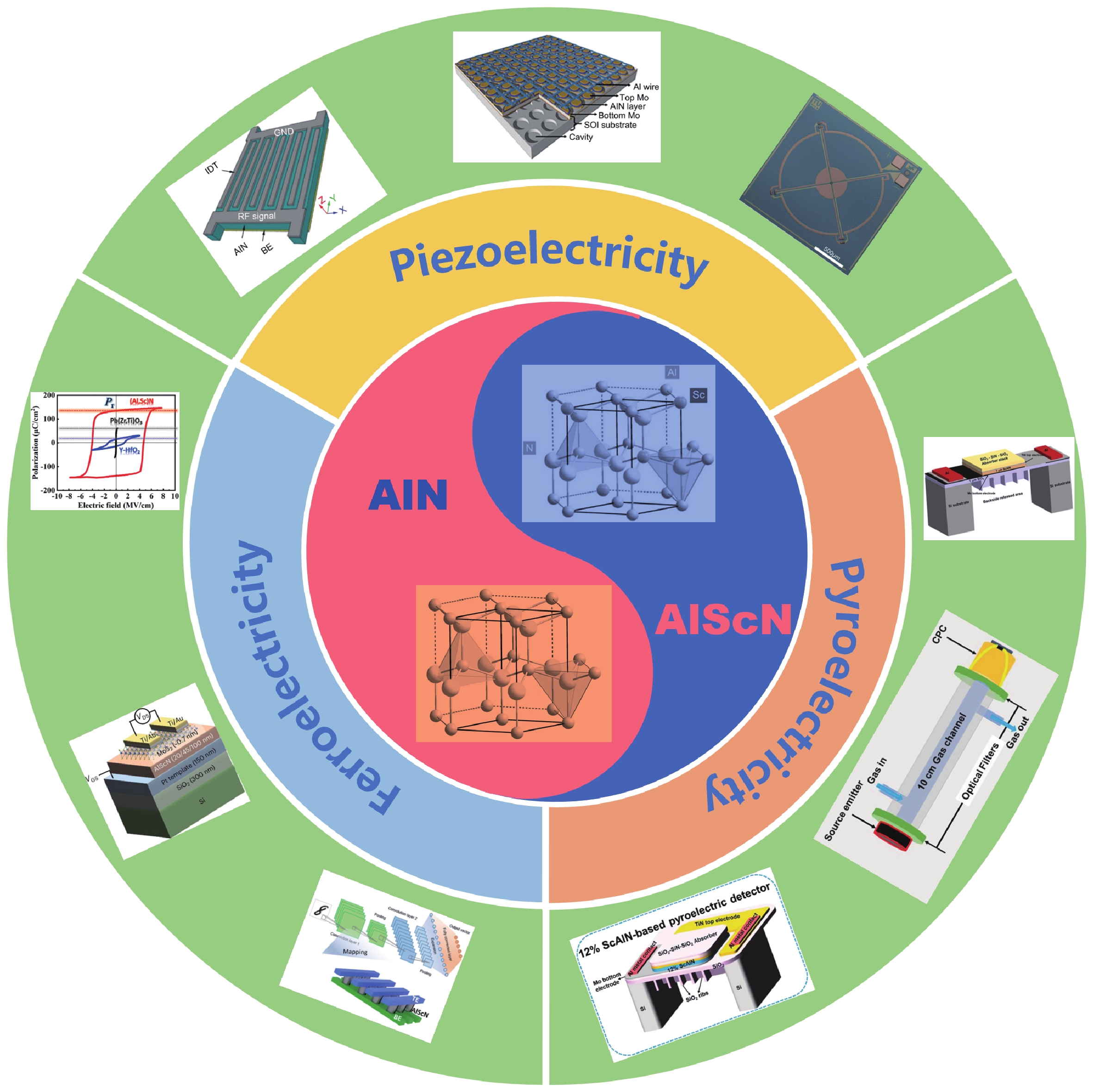
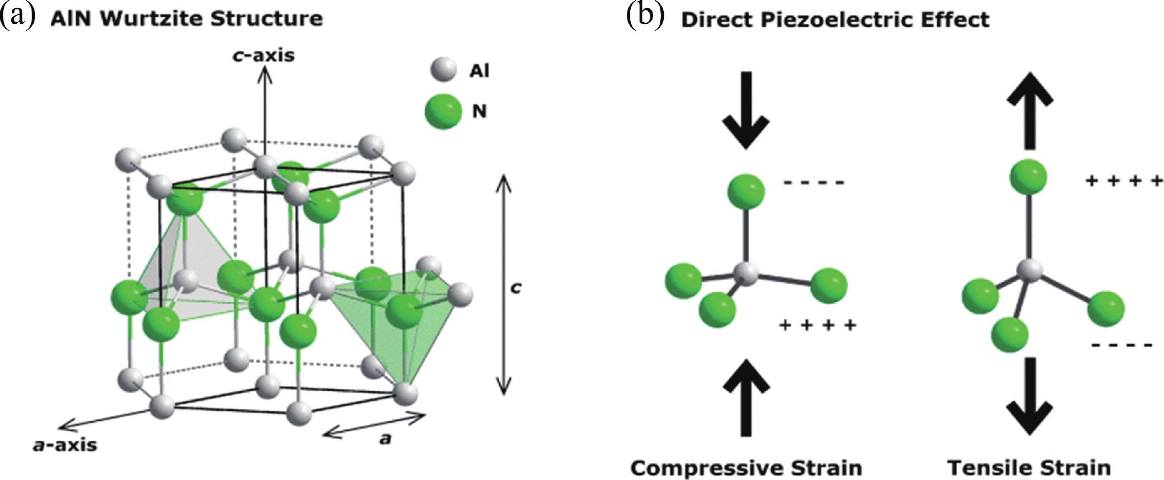
Aluminum scandium nitride (AlScN), an emerging Ⅲ-nitride semiconductor material, has attracted significant attention in recent years due to its exceptional piezoelectric properties, high thermal stability, tunable bandgap, and excellent compatibility with micro/nano fabrication. This paper systematically reviews the crystal structure, fundamental properties, and property modulation mechanisms of AlScN. It also summarizes recent progress in micro/nano fabrication technologies, including deposition, etching, and device integration. Furthermore, the applications of AlScN in diverse fields such as micro-electromechanical systems (MEMS), RF communications, energy conversion, optoelectronics and sensors are discussed. Finally, current challenges and promising future research directions for AlScN are outlined.

Key words: aluminum scandium nitridematerial propertiesmicro/nano fabricationdevice integration


[1]
Wang W B, Mayrhofer P M, He X L, et al. High performance AlScN thin film based surface acoustic wave devices with large electromechanical coupling coefficient. Appl Phys Lett, 2014, 105(13), 133502 doi: 10.1063/1.4896853
[2]
Su J X, Niekiel F, Fichtner S, et al. AlScN-based MEMS magnetoelectric sensor. Appl Phys Lett, 2020, 117(13), 132903 doi: 10.1063/5.0022636
[3]
Kim K H, Song S, Kim B, et al. Tuning polarity in WSe2/AlScN FeFETs via contact engineering. ACS Nano, 2024, 18(5), 4180 doi: 10.1021/acsnano.3c09279
[4]
Zywitzki O, Modes T, Barth S, et al. Effect of scandium content on structure and piezoelectric properties of AlScN films deposited by reactive pulse magnetron sputtering. Surf & Coat Techol, 2017, 309(1), 417
[5]
Esteves G, Young T R, Tang Z C, et al. Al0.68Sc0.32N Lamb wave resonators with electromechanical coupling coefficients near 10.28%. Appl Phys Lett, 2021, 118(17), 171902 doi: 10.1063/5.0047647
[6]
Kanouni F, Arab F, Amara S, et al. The piezoelectricity of AlScN thin films under high-pressure regime. Phys Solid State, 2023, 65(2), 111
[7]
Ranu, Uthra B, Sinha R, et al. CMOS compatible pyroelectric materials for infrared detectors. Mater Sci Semicond Proc, 2022, 140, 106375 doi: 10.1016/j.mssp.2021.106375
[8]
Döring P, Krause S, Friesicke C, et al. Theoretical limits of the matching bandwidth and output power of AlScN-based HEMTs. IEEE Trans Electron Devices, 2024, 71(3), 1670 doi: 10.1109/TED.2023.3334224
[9]
Liu J Y, Ma J N, Du X, et al. Tailoring p-type conductivity of aluminum nitride via transition metal and fluorine doping. J Alloys Compd, 2021, 862, 158017 doi: 10.1016/j.jallcom.2020.158017
[10]
Zhang H, Wang Y, Wang L H, et al. Process control monitor (PCM) for simultaneous determination of the piezoelectric coefficients d31 and d33 of AlN and AlScN Thin Films. Micromachines, 2022, 13(4), 581 doi: 10.3390/mi13040581
[11]
Su J X, Fichtner S, Ghori M Z, et al. Growth of highly c-axis oriented AlScN films on commercial substrates. Micromachines, 2022, 13(5), 783 doi: 10.3390/mi13050783
[12]
Sui W, Wang H R, Lee J, et al. AlScN-on-SiC thin film micromachined resonant transducers operating in high-temperature environment up to 600 °C. Adv Funct Mater, 2022, 32(34), 2202204 doi: 10.1002/adfm.202202204
[13]
Casamento J, Nomoto K, Nguyen T S, et al. FerroHEMTs: High-current and high-speed all-epitaxial AlScN/GaN ferroelectric transistors. 2022 International Electron Devices Meeting (IEDM), 2022, 11
[14]
Clement M, Felmetsger V, Mirea T, et al. Reactive sputtering of AlScN thin films with variable Sc content on 200 mm wafers. 2018 European Frequency and Time Forum (EFTF). Turin, Italy. IEEE, 2018, 13
[15]
Shao S, Luo Z F, Lu Y, et al. High quality co-sputtering AlScN thin films for piezoelectric Lamb-wave resonators. J Microelectromech Syst, 2022, 31(3), 328 doi: 10.1109/JMEMS.2022.3161055
[16]
Luo Z, Shao S, Wu T. Characterization of AlN and AlScN film ICP etching for micro/nano fabrication. Microelectron Eng, 2021, 242, 111530
[17]
Wang L, Chen S M, Zhang J Y, et al. High performance 33.7 GHz surface acoustic wave nanotransducers based on AlScN/diamond/Si layered structures. Appl Phys Lett, 2018, 113(9), 093503 doi: 10.1063/1.5046113
[18]
Liu X W, Wang D X, Kim K H, et al. Post-CMOS compatible aluminum scandium nitride/2D channel ferroelectric field-effect-transistor memory. Nano Lett, 2021, 21(9), 3753 doi: 10.1021/acs.nanolett.0c05051
[19]
Kim K H, Oh S, Fiagbenu M M A, et al. Scalable CMOS back-end-of-line-compatible AlScN/two-dimensional channel ferroelectric field-effect transistors. Nat Nanotechnol, 2023, 18(9), 1044 doi: 10.1038/s41565-023-01399-y
[20]
Shao S, Luo Z F, Wu T. High figure-of-merit Lamb wave resonators based on Al0.7Sc0.3N thin film. IEEE Electron Device Lett, 2021, 42(9), 1378 doi: 10.1109/LED.2021.3100036
[21]
Bette S, Fichtner S, Bröker S, et al. Infrared-laser based characterization of the pyroelectricity in AlScN thin-films. Thin Solid Films, 2019, 692(31), 137623
[22]
Hussein H M, Ben A F, Venditti A, et al. Parametric frequency comb generator based AlScN MEMS IR detector for low-power and high-performance applications. Image Sensing Technologies: Materials, Devices, Systems, and Applications XI, 2024, 13030
[23]
Doko S, Matsui N, Irisawa T, et al. Thickness dependence of ferroelectricity for thin (Al0.9Sc0.1)N-based FeRAM. IEEE International Meeting for Furture of Electron Devices, Kansai (IMFEDK), 2024, 1
[24]
Dai X H, Hua Q L, Jiang C S, et al. Artificial synapse based on a tri-layer AlN/AlScN/AlN stacked memristor for neuromorphic computing. Nano Energy, 2024, 124, 109473 doi: 10.1016/j.nanoen.2024.109473
[25]
Tahhan M B, Logan J A, Hardy M T, et al. Passivation schemes for ScAlN-barrier mm-wave high electron mobility transistors. IEEE Trans Electron Devices, 2022, 69(3), 962 doi: 10.1109/TED.2021.3140016
[26]
Yang J Y, Oh S Y, Yeom M J, et al. Pulsed E-/D-mode switchable GaN HEMTs with a ferroelectric AlScN gate dielectric. IEEE Electron Device Lett, 2023, 44(8), 1260 doi: 10.1109/LED.2023.3287913
[27]
Liu Z, Shao Z, Cao Y, et al. Strain engineering boosts piezo-/ferroelectricity in AlScN alloy: insights from first-principles calculations. Chem Mater, 2025, 37(15), 6026 doi: 10.1021/acs.chemmater.5c01383
[28]
Ruiz E, Alvarez S, Alemany P. Electronic structure and properties of AlN. Phys Rev B Condens Matter, 1994, 49(11), 7115 doi: 10.1103/PhysRevB.49.7115
[29]
Tsai S L, Hoshii T, Wakabayashi H, et al. Room-temperature deposition of a poling-free ferroelectric AlScN film by reactive sputtering. Appl Phys Lett, 2021, 118(8), 082902 doi: 10.1063/5.0035335
[30]
Yang H Q, Sun J, Wang H J, et al. A review of oriented wurtzite-structure aluminum nitride films. J Alloys Compd, 2024, 989(1), 174330
[31]
Xu X H, Wu H S, Zhang C J, et al. Morphological properties of AlN piezoelectric thin films deposited by DC reactive magnetron sputtering. Thin Solid Films, 2001, 388(1), 62
[32]
Yokoyama T, Iwazaki Y, Nishihara T, et al. Analysis on electromechanical coupling coefficients in AlN-based bulk acoustic wave resonators based on first-principle calculations. 2012 IEEE International Ultrasonics Symposium, 2012, 551
[33]
Yan X F, Wang B W, Yan H J, et al. Orbital hybridization and defective states of vacancy defects in AlN. Mater Today Commun, 2024, 39(1), 109063
[34]
Gruber J B, Vetter U, Burdick G W, et al. Analysis of the spectra of trivalent erbium in multiple sites of hexagonal aluminum nitride. Opt Mater Express, 2012, 2(9), 1186 doi: 10.1364/OME.2.001186
[35]
Dorenbos P, Kolk E. Location of lanthanide impurity energy levels in the III-V semiconductor AlxGa1-xN (0 ≤ x ≤ 1). Opt Mater, 2008, 30(7), 1052 doi: 10.1016/j.optmat.2007.05.019
[36]
Tasnádi F, Alling B, Höglund C, et al. Origin of the anomalous piezoelectric response in wurtzite ScxAl1-xN alloys. Phys Rev Lett, 2010, 104(13), 137601 doi: 10.1103/PhysRevLett.104.137601
[37]
Akiyama M, Kamohara T, Kano K, et al. Enhancement of piezoelectric response in scandium aluminum nitride alloy thin films prepared by dual reactive cosputtering. Adv Mater, 2009, 21(5), 593 doi: 10.1002/adma.200802611
[38]
Deng R P, Evans S R, Gall D. Bandgap in Al1−xScxN. Appl Phys Lett, 2013, 102(11), 112103 doi: 10.1063/1.4795784
[39]
Kasu M, Kobayashi N. Heavily Si-doped AlN electron field emitters. Proceedings of the International Workshop on Nitride Semiconductors, 2000, 1, 993
[40]
Jamil T, Mazumder A A, Rahman M, et al. Si-doped AlN using pulsed metalorganic chemical vapor deposition and doping. Appl Phys Express, 2025, 18(2), 025501 doi: 10.35848/1882-0786/adadc2
[41]
Peng Y T, Xia C X, Zhang H, et al. Tunable electronic structures of p-type Mg doping in AlN nanosheet. J Appl Phys, 2014, 116(4), 044306 doi: 10.1063/1.4891238
[42]
Nonaka K, Asai T, Nagamatsu K, et al. Defects in highly Mg-doped AlN. Phys Status Solidi A, 2010, 207(6), 1299 doi: 10.1002/pssa.200983504
[43]
Ahmad H, Engel Z, Matthews C M, et al. P-type AlN based heteroepitaxial diodes with Schottky, Pin, and junction barrier Schottky character achieving significant breakdown performance. J Appl Phys, 2021, 130(19), 195702 doi: 10.1063/5.0069539
[44]
Iwazaki Y, Yokoyama T, Nishihara T, et al. Highly enhanced piezoelectric property of Co-doped AlN. Appl Phys Express, 2015, 8(6), 061501 doi: 10.7567/APEX.8.061501
[45]
Pinto R M R, Gund V, Dias R A, et al. CMOS-integrated aluminum nitride MEMS: A review. J Microelectromech Syst, 2022, 31(4), 500 doi: 10.1109/JMEMS.2022.3172766
[46]
Trolier M S. Crystal chemistry of piezoelectric materials. Springer US, 2008
[47]
Nersisyan H H, Lee J H, Kim H Y, et al. Morphological diversity of AlN nano- and microstructures: Synthesis, growth orientations and theoretical modelling. Int Mater Rev, 2020, 65(6), 323 doi: 10.1080/09506608.2019.1641651
[48]
Barth S, Schreiber T, Cornelius S, et al. High rate deposition of piezoelectric AlScN films by reactive magnetron sputtering from AlSc alloy targets on large area. Micromachines, 2022, 13(10), 1561 doi: 10.3390/mi13101561
[49]
Barth S, Bartzsch H, Gloess D, et al. Sputter deposition of stress-controlled piezoelectric AlN and AlScN films for ultrasonic and energy harvesting applications. IEEE Trans Ultrason Ferroelectr Freq Contr, 2014, 61(8), 1329 doi: 10.1109/TUFFC.2014.3040
[50]
Shao W J, Zhang M C, Wang X P, et al. What you need to know for growth of AlScN thin film via atomic layer deposition? 2024 IEEE International Conference on IC Design and Technology (ICICDT), 2024, 1
[51]
Tanim M M H, Hasan M T, Ye Z, et al. Atomic layer deposition and characterization of scandium aluminum nitride. Appl Phys Lett, 2025, 127(3), 032109 doi: 10.1063/5.0278222
[52]
Manz C, Leone S, Kirste L, et al. Improved AlScN/GaN heterostructures grown by metal-organic chemical vapor deposition. Semicond Sci Technol, 2021, 36(3), 034003 doi: 10.1088/1361-6641/abd924
[53]
Leone S, Ligl J, Manz C, et al. Metal-organic chemical vapor deposition of aluminum scandium nitride. Physica Rapid Research Ltrs, 2020, 14, 1900535 doi: 10.1002/pssr.201900535
[54]
Hardy M T, Meyer D J. Chapter one-epitaxial ScAlN: Transistors through high ScN fraction thin films. Emerging Ferroelectric Materials and Devices. Amsterdam: Elsevier, 2023, 1
[55]
Fei C L, Liu X L, Zhu B P, et al. AlN piezoelectric thin films for energy harvesting and acoustic devices. Nano Energy, 2018, 51, 146 doi: 10.1016/j.nanoen.2018.06.062
[56]
Barth S, Bartzsch H, Glöss D, et al. Effect of process parameters on structure and piezoelectric properties of AlN and AlxSc1−xN films deposited by pulsed magnetron sputtering. 2014 IEEE International Ultrasonics Symposium (IUS), 2014, 769
[57]
Patidar J, Thorwarth K, Schmitz-Kempen T, et al. Deposition of highly crystalline AlScN thin films using synchronized high-power impulse magnetron sputtering: From combinatorial screening to piezoelectric devices. Phys Rev Mater, 2024, 8(9), 095001 doi: 10.1103/PhysRevMaterials.8.095001
[58]
Lu Y, Reusch M, Kurz N, et al. Surface morphology and microstructure of pulsed DC magnetron sputtered piezoelectric AlN and AlScN thin films. Phys Status Solidi A, 2018, 215(9), 1700559 doi: 10.1002/pssa.201700559
[59]
Zhang W L, Li J G, Fang J B, et al. Atomic layer deposited high quality AlN thin films for efficient thermal management. J Mater Chem A, 2023, 11(40), 21846 doi: 10.1039/D3TA04618D
[60]
Shih H Y, Lee W H, Kao W C, et al. Low-temperature atomic layer epitaxy of AlN ultrathin films by layer-by-layer, in-situ atomic layer annealing. Sci Rep, 2017, 7, 39717 doi: 10.1038/srep39717
[61]
Wolff N, Schönweger G, Streicher I, et al. Demonstration and STEM analysis of ferroelectric switching in MOCVD-grown single crystalline Al0.85Sc0.15N. Adv Phys Res, 2024, 3(5), 2300113 doi: 10.1002/apxr.202300113
[62]
Streicher I, Leone S, Kirste L, et al. Enhanced AlScN/GaN heterostructures grown with a novel precursor by metal-organic chemical vapor deposition. Physica Rapid Research Ltrs, 2023, 17(2), 2200387 doi: 10.1002/pssr.202200387
[63]
Salhi R, Deschanvres J L. Efficient upconversion in Er3+ doped Y2O3/Si thin film deposited by aerosol UV-assisted MOCVD process. J Lumin, 2016, 170, 231 doi: 10.1016/j.jlumin.2015.10.027
[64]
Rathkanthiwar S, Kalra A, Muralidharan R, et al. V-pits-induced photoresponse enhancement in AlGaN UV-B photodetectors on Si (111). IEEE Trans on Electron Devices, 2020, 67(10), 4281 doi: 10.1109/TED.2020.3014852
[65]
Adnaan M, Chang S-C, Li H, et al. Design considerations for sub-1-V 1T1C FeRAM memory circuits. IEEE J Explor Solid State Comput Devices Circuits, 2024, 10, 107 doi: 10.1109/JXCDC.2024.3488578
[66]
Wang D, Wang P, Mondal S, et al. An epitaxial ferroelectric ScAlN/GaN heterostructure memory. Adv Electron Mater, 2022, 8(9), 2200005 doi: 10.1002/aelm.202200005
[67]
Wang P, Wang D, Wang B Y, et al. N-polar ScAlN and HEMTs grown by molecular beam epitaxy. Appl Phys Lett, 2021, 119(8), 082101 doi: 10.1063/5.0055851
[68]
Zhuang D, Edgar J H. Wet etching of GaN, AlN, and SiC: a review. Mater Sci Eng R Rep, 2005, 48(1), 1 doi: 10.1016/j.mser.2004.11.002
[69]
Guo W, Kirste R, Bryan I, et al. KOH based selective wet chemical etching of AlN, AlxGa1−xN, and GaN crystals: A way towards substrate removal in deep ultraviolet-light emitting diode. Appl Phys Lett, 2015, 106(8), 082110 doi: 10.1063/1.4913705
[70]
Bespalova K, Österlund E, Ross G, et al. Characterization of AlScN-based multilayer systems for piezoelectric micromachined ultrasound transducer (PMUT) fabrication. J Microelectromech Syst, 2021, 30(2), 290 doi: 10.1109/JMEMS.2021.3056928
[71]
Tang Z C, Esteves G, Zheng J, et al. Vertical and lateral etch survey of ferroelectric AlN/Al1−xScxN in aqueous KOH solutions. Micromachines, 2022, 13(7), 1066 doi: 10.3390/mi13071066
[72]
Yang J, Si C W, Han G W, et al. Researching the aluminum nitride etching process for application in MEMS resonators. Micromachines, 2015, 6(2), 281 doi: 10.3390/mi6020281
[73]
Li J, Xu X, Li Y, et al. Electrically tunable GHz acoustic waveguide using Al0.7Sc0.3N thin film. Appl Phys Lett, 2025, 126(9), 092201 doi: 10.1063/5.0257586
[74]
Huang W X, Xia L P, Li J W, et al. Acousto-optic modulation on silicon-aluminum nitride hybrid-integrated platform for cryogenic applications. Nano Lett, 2025, 25(13), 5117 doi: 10.1021/acs.nanolett.4c05680
[75]
Shao S, Luo Z F, Wu T. Electro-acoustic phase modulator based on AlScN thin film. IEEE Electron Device Lett, 2023, 44(5), 817 doi: 10.1109/LED.2023.3259440
[76]
Bian K W, Li Z Y, Liu Y S, et al. Demonstration of acousto-optical modulation based on a thin-film AlScN photonic platform. Photon Res, 2024, 12(6), 1138 doi: 10.1364/PRJ.517719
[77]
Huang C K, Shi H T, Yu L F, et al. Acousto-optic modulation in silicon waveguides based on piezoelectric aluminum scandium nitride film. Adv Opt Mater, 2022, 10(6), 2102334 doi: 10.1002/adom.202102334
[78]
Popa D, Udrea F. Towards integrated mid-infrared gas sensors. Sensors, 2019, 19(9), 2076 doi: 10.3390/s19092076
[79]
Chattopadhyay T, Bhattacharyya P. Higher order nonlinearity and synchronization of quantum cascade lasers. Optoelectron Lett, 2011, 7(3), 186 doi: 10.1007/s11801-011-1013-z
[80]
Fujita H, Ueno K, Morohara O, et al. AlInSb mid-infrared LEDs of high luminous efficiency for gas sensors. Phys Status Solidi A, 2018, 215(8), 1700449 doi: 10.1002/pssa.201700449
[81]
Lochbaum A, Fedoryshyn Y, Dorodnyy A, et al. On-chip narrowband thermal emitter for mid-IR optical gas sensing. ACS Photonics, 2017, 4(6), 1371 doi: 10.1021/acsphotonics.6b01025
[82]
Sun W X, Kou X, Zhou J R, et al. AlScN ferroelectric diode enabled CAM with 4F2 cell size and low thermal budget (330 °C). IEEE Electron Device Lett, 2025, 46(4), 568 doi: 10.1109/LED.2025.3538669
[83]
Kim K D, Yeom M K, Park H S, et al. Proximity-induced ferroelectric switching in wurtzite/fluorite bilayers for high-performance ferroelectric field-effect transistor. Adv Mater, 2025, e09088
[84]
Ng D K T, Wu G Q, Zhang T T, et al. Considerations for an 8-inch wafer-level CMOS compatible AlN pyroelectric 5−14 μm wavelength IR detector towards miniature integrated photonics gas sensors. J Microelectromech Syst, 2020, 29(5), 1199 doi: 10.1109/JMEMS.2020.3015378
[85]
Ng D K T, Ho C P, Xu L F, et al. NDIR CO2 gas sensing using CMOS compatible MEMS ScAlN-based pyroelectric detector. Sens Actuat B Chem, 2021, 346, 130437 doi: 10.1016/j.snb.2021.130437
[86]
Beaucejour R, Roebisch V, Kochhar A, et al. Controlling residual stress and suppression of anomalous grains in aluminum scandium nitride films grown directly on silicon. J Microelectromech S, 2022, 31(4), 604 doi: 10.1109/JMEMS.2022.3167430
[87]
Lu H D, Schönweger G, Petraru A, et al. Domain dynamics and resistive switching in ferroelectric Al1-xScxN thin film capacitors. Adv Funct Mater, 2024, 34(28), 2315169 doi: 10.1002/adfm.202315169
[88]
Qin H M, He N, Han C, et al. Perspectives of ferroelectric wurtzite AlScN: Material characteristics, preparation, and applications in advanced memory devices. Nanomaterials, 2024, 14(11), 986 doi: 10.3390/nano14110986
[89]
Mikolajick T, Dehm C, Hartner W, et al. FeRAM technology for high density applications. Microelectron Reliab, 2001, 41(7), 947 doi: 10.1016/S0026-2714(01)00049-X
[90]
Lee T Y, Cho J W, Lim H H, et al. Polarity-dependent fatigue behavior of domain switching kinetics in textured ferroelectric Al0.72Sc0.28N thin films. J Alloys Compd, 2025, 1034, 181305 doi: 10.1016/j.jallcom.2025.181305
[91]
Zhang Y L, Zhu Q X, Tian B B, et al. New-generation ferroelectric AlScN materials. Nano-Micro Letters, 2024, 16(1), 227 doi: 10.1007/s40820-024-01441-1
[92]
Wang L Y, Cheng J H, Qu K, et al. Aluminum-nitride-based semiconductors: Growth processes, ferroelectric properties, and performance enhancements. Inorganics, 2025, 13(2), 29 doi: 10.3390/inorganics13020029
Fig. 1.  (Color online) Schematic diagram of AlScN material properties, micro-nano processing and its diverse applications[1719].

Fig. 2.  (Color online) (a) Crystal structure of wurtzite type aluminum nitride (AlN); (b) schematic diagrams of Al−N bonds of type B1 and B2[30].

Fig. 3.  (Color online) (a) AlScN with hexagonal wurtzite structure, where red color represents Al or Sc atoms, blue color represents N atoms. (b) Tetrahedral structure with bond angle[15].

Fig. 4.  (Color online) Formation energies of the dopant elements in AlN obtained from ab initio calculations[44].

Fig. 5.  (Color online) (a) Illustration of the wurtzite structure of AlN and the lattice parameters. (b) In AlN, the origin of the direct piezoelectric effect is in the displacement of the charge centers when the material is strained[45].

Fig. 6.  (Color online) (a) Based on the most promising synthesis schemes from the combinatorial screening, single-phase Al80Sc20N films are synthesized and piezoelectric devices are fabricated with Pt top and bottom electrodes[57]; (b) number of abnormal grains in an area of 100 µm2 as a function of N2 concentration and target-to-substrate distance (inset)[58].

Fig. 7.  (Color online) (a) The schematic diagram of the modified ALD cycles for atomic layer epitaxy, with an additional step (5) of the Ar plasma treatment for In-situ atomic layer annealing (ALA); (b) schematic diagram of a super-cycle (take AlN: Sc as an example)[60].

Fig. 8.  (Color online) (a) ABF-STEM investigation of the pristine MOCVD-grown Al0.85Sc0.15N layer (center image). The atomic polarization of the pristine film under the capacitor is identified to grow completely M-polar from the bottom interface (left image) toward the top electrode (right image); (b) ABF-STEM image showing the cone-like domain pattern in the switched region of the film in direct comparison to the pristine region[61].

Fig. 9.  (Color online) (a) ScAlN-GaN thin film structure grown on GaN; (b) XRD results of ScAlN/GaN films[66].

Fig. 10.  (Color online) (a) Al0.95Sc0.05N etched for 10 s in 30% KOH at 45 °C; (b) Al0.85Sc0.15N etched for 2.5 min in 30% KOH at 65 °C; (c) vertical etch rate of Al1−xScxN in 30% KOH at 45 °C; (d) lateral etch rate of Al1−xScxN in 30% KOH at 45 °C[71].

Fig. 11.  (Color online) (a) and (b) The optimized profile is higher than 77°, while the etching surface is very smooth and clean with 550 W ICP power, 80 W RF power and the flow rate of Cl2/BCl3/N2 are 15/30/5 sccm[16]; (c) SEM image of ICP etch profile for Al0.78Sc0.22N film, (d) SEM of the Lamb-wave resonator with floating bottom electrode[15].

Fig. 12.  (Color online) Inline measurement of the thickness and uniformity of the device film layer. (a) W wafer map diagram of the lower electrode; (b) piezoelectric layer AlScN wafer map diagram; (c) upper electrode Mo wafer map diagram; (d) device film stack diagram.

Fig. 13.  (Color online) AO devices based on thin-film AlScN photonic platform. (a) Cross-sectional view of the device. It consists of an AlScN ridge waveguide with a width (W) and an etching depth of 220 nm, along with the aluminum IDTs; (b) numerical simulation results of the normalized electric field and strain field profiles[76]; (c) 3D model of the proposed AO device; (d) phase-matching diagram with dispersion curve of optical wave (red line) and incident acoustic wave (green arrow), together with the x-component electric field profiles of the optical mode TE0 in the waveguide[77].

Fig. 14.  (Color online) Schematic of (a) AlScN-based pyroelectric detector device for CO2 gas sensing; (b) gas sensing approach using AlScN-based pyroelectric detector device[81].

Fig. 15.  (Color online) (a) Typical structure of 1T-1C DRAM; (b) basic unit structure of Flash memory; (c) typical structure of 1T-1C FeRAM; (d) two different structures of FeFET. The structure on the upper side is similar to a floating gate transistor, while for the lower structure, the gate is on the lower substrate, and 2D material is used as the channel; (e) schematic diagram of FTJ structure and barrier height determined by polarization state[88].

Table 1.   Typical parameter comparison of AlScN and AlN.

Parameter AlN AlScN Ref.
Piezoelectric coefficient (d33) 5−5.5 pC/N 24−28 pC/N [4]
Electromechanical coupling (Kt2) 6−7% ~25% (for 40% Sc) [5]
Dielectric constant (ε) ~10.1 12.8−17 [6]
Bandgap (Eg) ~6.2 eV 3.2−6.2 eV (Tunable) [10, 11]
Pyroelectric coefficient (p) 6−8 μC/(m2·K) 15−20 μC/ (m2·K) [21]
Remnant polarization (Pr) / >100 μC/cm2 [23, 24]
Coercive field (Ec) / ~5 MV/cm [23, 24]
DownLoad: CSV

Table 2.   Comparison of alternative methods for AlScN deposition.

Method Feature Temperature range Deposition rate Uniformity Ref.
PVD Low cost, good uniformity RT−500 °C High <5% [48, 49]
ALD Atomic-level accuracy, suitable for ultra-thin stacked structures 200−300 °C low <2% [50, 51]
MOCVD High crystalline quality, high yield >900 °C Low <3% [52, 53]
MBE Atomic-level control, superior crystalline <800 °C low <1% [54]
DownLoad: CSV
[1]
Wang W B, Mayrhofer P M, He X L, et al. High performance AlScN thin film based surface acoustic wave devices with large electromechanical coupling coefficient. Appl Phys Lett, 2014, 105(13), 133502 doi: 10.1063/1.4896853
[2]
Su J X, Niekiel F, Fichtner S, et al. AlScN-based MEMS magnetoelectric sensor. Appl Phys Lett, 2020, 117(13), 132903 doi: 10.1063/5.0022636
[3]
Kim K H, Song S, Kim B, et al. Tuning polarity in WSe2/AlScN FeFETs via contact engineering. ACS Nano, 2024, 18(5), 4180 doi: 10.1021/acsnano.3c09279
[4]
Zywitzki O, Modes T, Barth S, et al. Effect of scandium content on structure and piezoelectric properties of AlScN films deposited by reactive pulse magnetron sputtering. Surf & Coat Techol, 2017, 309(1), 417
[5]
Esteves G, Young T R, Tang Z C, et al. Al0.68Sc0.32N Lamb wave resonators with electromechanical coupling coefficients near 10.28%. Appl Phys Lett, 2021, 118(17), 171902 doi: 10.1063/5.0047647
[6]
Kanouni F, Arab F, Amara S, et al. The piezoelectricity of AlScN thin films under high-pressure regime. Phys Solid State, 2023, 65(2), 111
[7]
Ranu, Uthra B, Sinha R, et al. CMOS compatible pyroelectric materials for infrared detectors. Mater Sci Semicond Proc, 2022, 140, 106375 doi: 10.1016/j.mssp.2021.106375
[8]
Döring P, Krause S, Friesicke C, et al. Theoretical limits of the matching bandwidth and output power of AlScN-based HEMTs. IEEE Trans Electron Devices, 2024, 71(3), 1670 doi: 10.1109/TED.2023.3334224
[9]
Liu J Y, Ma J N, Du X, et al. Tailoring p-type conductivity of aluminum nitride via transition metal and fluorine doping. J Alloys Compd, 2021, 862, 158017 doi: 10.1016/j.jallcom.2020.158017
[10]
Zhang H, Wang Y, Wang L H, et al. Process control monitor (PCM) for simultaneous determination of the piezoelectric coefficients d31 and d33 of AlN and AlScN Thin Films. Micromachines, 2022, 13(4), 581 doi: 10.3390/mi13040581
[11]
Su J X, Fichtner S, Ghori M Z, et al. Growth of highly c-axis oriented AlScN films on commercial substrates. Micromachines, 2022, 13(5), 783 doi: 10.3390/mi13050783
[12]
Sui W, Wang H R, Lee J, et al. AlScN-on-SiC thin film micromachined resonant transducers operating in high-temperature environment up to 600 °C. Adv Funct Mater, 2022, 32(34), 2202204 doi: 10.1002/adfm.202202204
[13]
Casamento J, Nomoto K, Nguyen T S, et al. FerroHEMTs: High-current and high-speed all-epitaxial AlScN/GaN ferroelectric transistors. 2022 International Electron Devices Meeting (IEDM), 2022, 11
[14]
Clement M, Felmetsger V, Mirea T, et al. Reactive sputtering of AlScN thin films with variable Sc content on 200 mm wafers. 2018 European Frequency and Time Forum (EFTF). Turin, Italy. IEEE, 2018, 13
[15]
Shao S, Luo Z F, Lu Y, et al. High quality co-sputtering AlScN thin films for piezoelectric Lamb-wave resonators. J Microelectromech Syst, 2022, 31(3), 328 doi: 10.1109/JMEMS.2022.3161055
[16]
Luo Z, Shao S, Wu T. Characterization of AlN and AlScN film ICP etching for micro/nano fabrication. Microelectron Eng, 2021, 242, 111530
[17]
Wang L, Chen S M, Zhang J Y, et al. High performance 33.7 GHz surface acoustic wave nanotransducers based on AlScN/diamond/Si layered structures. Appl Phys Lett, 2018, 113(9), 093503 doi: 10.1063/1.5046113
[18]
Liu X W, Wang D X, Kim K H, et al. Post-CMOS compatible aluminum scandium nitride/2D channel ferroelectric field-effect-transistor memory. Nano Lett, 2021, 21(9), 3753 doi: 10.1021/acs.nanolett.0c05051
[19]
Kim K H, Oh S, Fiagbenu M M A, et al. Scalable CMOS back-end-of-line-compatible AlScN/two-dimensional channel ferroelectric field-effect transistors. Nat Nanotechnol, 2023, 18(9), 1044 doi: 10.1038/s41565-023-01399-y
[20]
Shao S, Luo Z F, Wu T. High figure-of-merit Lamb wave resonators based on Al0.7Sc0.3N thin film. IEEE Electron Device Lett, 2021, 42(9), 1378 doi: 10.1109/LED.2021.3100036
[21]
Bette S, Fichtner S, Bröker S, et al. Infrared-laser based characterization of the pyroelectricity in AlScN thin-films. Thin Solid Films, 2019, 692(31), 137623
[22]
Hussein H M, Ben A F, Venditti A, et al. Parametric frequency comb generator based AlScN MEMS IR detector for low-power and high-performance applications. Image Sensing Technologies: Materials, Devices, Systems, and Applications XI, 2024, 13030
[23]
Doko S, Matsui N, Irisawa T, et al. Thickness dependence of ferroelectricity for thin (Al0.9Sc0.1)N-based FeRAM. IEEE International Meeting for Furture of Electron Devices, Kansai (IMFEDK), 2024, 1
[24]
Dai X H, Hua Q L, Jiang C S, et al. Artificial synapse based on a tri-layer AlN/AlScN/AlN stacked memristor for neuromorphic computing. Nano Energy, 2024, 124, 109473 doi: 10.1016/j.nanoen.2024.109473
[25]
Tahhan M B, Logan J A, Hardy M T, et al. Passivation schemes for ScAlN-barrier mm-wave high electron mobility transistors. IEEE Trans Electron Devices, 2022, 69(3), 962 doi: 10.1109/TED.2021.3140016
[26]
Yang J Y, Oh S Y, Yeom M J, et al. Pulsed E-/D-mode switchable GaN HEMTs with a ferroelectric AlScN gate dielectric. IEEE Electron Device Lett, 2023, 44(8), 1260 doi: 10.1109/LED.2023.3287913
[27]
Liu Z, Shao Z, Cao Y, et al. Strain engineering boosts piezo-/ferroelectricity in AlScN alloy: insights from first-principles calculations. Chem Mater, 2025, 37(15), 6026 doi: 10.1021/acs.chemmater.5c01383
[28]
Ruiz E, Alvarez S, Alemany P. Electronic structure and properties of AlN. Phys Rev B Condens Matter, 1994, 49(11), 7115 doi: 10.1103/PhysRevB.49.7115
[29]
Tsai S L, Hoshii T, Wakabayashi H, et al. Room-temperature deposition of a poling-free ferroelectric AlScN film by reactive sputtering. Appl Phys Lett, 2021, 118(8), 082902 doi: 10.1063/5.0035335
[30]
Yang H Q, Sun J, Wang H J, et al. A review of oriented wurtzite-structure aluminum nitride films. J Alloys Compd, 2024, 989(1), 174330
[31]
Xu X H, Wu H S, Zhang C J, et al. Morphological properties of AlN piezoelectric thin films deposited by DC reactive magnetron sputtering. Thin Solid Films, 2001, 388(1), 62
[32]
Yokoyama T, Iwazaki Y, Nishihara T, et al. Analysis on electromechanical coupling coefficients in AlN-based bulk acoustic wave resonators based on first-principle calculations. 2012 IEEE International Ultrasonics Symposium, 2012, 551
[33]
Yan X F, Wang B W, Yan H J, et al. Orbital hybridization and defective states of vacancy defects in AlN. Mater Today Commun, 2024, 39(1), 109063
[34]
Gruber J B, Vetter U, Burdick G W, et al. Analysis of the spectra of trivalent erbium in multiple sites of hexagonal aluminum nitride. Opt Mater Express, 2012, 2(9), 1186 doi: 10.1364/OME.2.001186
[35]
Dorenbos P, Kolk E. Location of lanthanide impurity energy levels in the III-V semiconductor AlxGa1-xN (0 ≤ x ≤ 1). Opt Mater, 2008, 30(7), 1052 doi: 10.1016/j.optmat.2007.05.019
[36]
Tasnádi F, Alling B, Höglund C, et al. Origin of the anomalous piezoelectric response in wurtzite ScxAl1-xN alloys. Phys Rev Lett, 2010, 104(13), 137601 doi: 10.1103/PhysRevLett.104.137601
[37]
Akiyama M, Kamohara T, Kano K, et al. Enhancement of piezoelectric response in scandium aluminum nitride alloy thin films prepared by dual reactive cosputtering. Adv Mater, 2009, 21(5), 593 doi: 10.1002/adma.200802611
[38]
Deng R P, Evans S R, Gall D. Bandgap in Al1−xScxN. Appl Phys Lett, 2013, 102(11), 112103 doi: 10.1063/1.4795784
[39]
Kasu M, Kobayashi N. Heavily Si-doped AlN electron field emitters. Proceedings of the International Workshop on Nitride Semiconductors, 2000, 1, 993
[40]
Jamil T, Mazumder A A, Rahman M, et al. Si-doped AlN using pulsed metalorganic chemical vapor deposition and doping. Appl Phys Express, 2025, 18(2), 025501 doi: 10.35848/1882-0786/adadc2
[41]
Peng Y T, Xia C X, Zhang H, et al. Tunable electronic structures of p-type Mg doping in AlN nanosheet. J Appl Phys, 2014, 116(4), 044306 doi: 10.1063/1.4891238
[42]
Nonaka K, Asai T, Nagamatsu K, et al. Defects in highly Mg-doped AlN. Phys Status Solidi A, 2010, 207(6), 1299 doi: 10.1002/pssa.200983504
[43]
Ahmad H, Engel Z, Matthews C M, et al. P-type AlN based heteroepitaxial diodes with Schottky, Pin, and junction barrier Schottky character achieving significant breakdown performance. J Appl Phys, 2021, 130(19), 195702 doi: 10.1063/5.0069539
[44]
Iwazaki Y, Yokoyama T, Nishihara T, et al. Highly enhanced piezoelectric property of Co-doped AlN. Appl Phys Express, 2015, 8(6), 061501 doi: 10.7567/APEX.8.061501
[45]
Pinto R M R, Gund V, Dias R A, et al. CMOS-integrated aluminum nitride MEMS: A review. J Microelectromech Syst, 2022, 31(4), 500 doi: 10.1109/JMEMS.2022.3172766
[46]
Trolier M S. Crystal chemistry of piezoelectric materials. Springer US, 2008
[47]
Nersisyan H H, Lee J H, Kim H Y, et al. Morphological diversity of AlN nano- and microstructures: Synthesis, growth orientations and theoretical modelling. Int Mater Rev, 2020, 65(6), 323 doi: 10.1080/09506608.2019.1641651
[48]
Barth S, Schreiber T, Cornelius S, et al. High rate deposition of piezoelectric AlScN films by reactive magnetron sputtering from AlSc alloy targets on large area. Micromachines, 2022, 13(10), 1561 doi: 10.3390/mi13101561
[49]
Barth S, Bartzsch H, Gloess D, et al. Sputter deposition of stress-controlled piezoelectric AlN and AlScN films for ultrasonic and energy harvesting applications. IEEE Trans Ultrason Ferroelectr Freq Contr, 2014, 61(8), 1329 doi: 10.1109/TUFFC.2014.3040
[50]
Shao W J, Zhang M C, Wang X P, et al. What you need to know for growth of AlScN thin film via atomic layer deposition? 2024 IEEE International Conference on IC Design and Technology (ICICDT), 2024, 1
[51]
Tanim M M H, Hasan M T, Ye Z, et al. Atomic layer deposition and characterization of scandium aluminum nitride. Appl Phys Lett, 2025, 127(3), 032109 doi: 10.1063/5.0278222
[52]
Manz C, Leone S, Kirste L, et al. Improved AlScN/GaN heterostructures grown by metal-organic chemical vapor deposition. Semicond Sci Technol, 2021, 36(3), 034003 doi: 10.1088/1361-6641/abd924
[53]
Leone S, Ligl J, Manz C, et al. Metal-organic chemical vapor deposition of aluminum scandium nitride. Physica Rapid Research Ltrs, 2020, 14, 1900535 doi: 10.1002/pssr.201900535
[54]
Hardy M T, Meyer D J. Chapter one-epitaxial ScAlN: Transistors through high ScN fraction thin films. Emerging Ferroelectric Materials and Devices. Amsterdam: Elsevier, 2023, 1
[55]
Fei C L, Liu X L, Zhu B P, et al. AlN piezoelectric thin films for energy harvesting and acoustic devices. Nano Energy, 2018, 51, 146 doi: 10.1016/j.nanoen.2018.06.062
[56]
Barth S, Bartzsch H, Glöss D, et al. Effect of process parameters on structure and piezoelectric properties of AlN and AlxSc1−xN films deposited by pulsed magnetron sputtering. 2014 IEEE International Ultrasonics Symposium (IUS), 2014, 769
[57]
Patidar J, Thorwarth K, Schmitz-Kempen T, et al. Deposition of highly crystalline AlScN thin films using synchronized high-power impulse magnetron sputtering: From combinatorial screening to piezoelectric devices. Phys Rev Mater, 2024, 8(9), 095001 doi: 10.1103/PhysRevMaterials.8.095001
[58]
Lu Y, Reusch M, Kurz N, et al. Surface morphology and microstructure of pulsed DC magnetron sputtered piezoelectric AlN and AlScN thin films. Phys Status Solidi A, 2018, 215(9), 1700559 doi: 10.1002/pssa.201700559
[59]
Zhang W L, Li J G, Fang J B, et al. Atomic layer deposited high quality AlN thin films for efficient thermal management. J Mater Chem A, 2023, 11(40), 21846 doi: 10.1039/D3TA04618D
[60]
Shih H Y, Lee W H, Kao W C, et al. Low-temperature atomic layer epitaxy of AlN ultrathin films by layer-by-layer, in-situ atomic layer annealing. Sci Rep, 2017, 7, 39717 doi: 10.1038/srep39717
[61]
Wolff N, Schönweger G, Streicher I, et al. Demonstration and STEM analysis of ferroelectric switching in MOCVD-grown single crystalline Al0.85Sc0.15N. Adv Phys Res, 2024, 3(5), 2300113 doi: 10.1002/apxr.202300113
[62]
Streicher I, Leone S, Kirste L, et al. Enhanced AlScN/GaN heterostructures grown with a novel precursor by metal-organic chemical vapor deposition. Physica Rapid Research Ltrs, 2023, 17(2), 2200387 doi: 10.1002/pssr.202200387
[63]
Salhi R, Deschanvres J L. Efficient upconversion in Er3+ doped Y2O3/Si thin film deposited by aerosol UV-assisted MOCVD process. J Lumin, 2016, 170, 231 doi: 10.1016/j.jlumin.2015.10.027
[64]
Rathkanthiwar S, Kalra A, Muralidharan R, et al. V-pits-induced photoresponse enhancement in AlGaN UV-B photodetectors on Si (111). IEEE Trans on Electron Devices, 2020, 67(10), 4281 doi: 10.1109/TED.2020.3014852
[65]
Adnaan M, Chang S-C, Li H, et al. Design considerations for sub-1-V 1T1C FeRAM memory circuits. IEEE J Explor Solid State Comput Devices Circuits, 2024, 10, 107 doi: 10.1109/JXCDC.2024.3488578
[66]
Wang D, Wang P, Mondal S, et al. An epitaxial ferroelectric ScAlN/GaN heterostructure memory. Adv Electron Mater, 2022, 8(9), 2200005 doi: 10.1002/aelm.202200005
[67]
Wang P, Wang D, Wang B Y, et al. N-polar ScAlN and HEMTs grown by molecular beam epitaxy. Appl Phys Lett, 2021, 119(8), 082101 doi: 10.1063/5.0055851
[68]
Zhuang D, Edgar J H. Wet etching of GaN, AlN, and SiC: a review. Mater Sci Eng R Rep, 2005, 48(1), 1 doi: 10.1016/j.mser.2004.11.002
[69]
Guo W, Kirste R, Bryan I, et al. KOH based selective wet chemical etching of AlN, AlxGa1−xN, and GaN crystals: A way towards substrate removal in deep ultraviolet-light emitting diode. Appl Phys Lett, 2015, 106(8), 082110 doi: 10.1063/1.4913705
[70]
Bespalova K, Österlund E, Ross G, et al. Characterization of AlScN-based multilayer systems for piezoelectric micromachined ultrasound transducer (PMUT) fabrication. J Microelectromech Syst, 2021, 30(2), 290 doi: 10.1109/JMEMS.2021.3056928
[71]
Tang Z C, Esteves G, Zheng J, et al. Vertical and lateral etch survey of ferroelectric AlN/Al1−xScxN in aqueous KOH solutions. Micromachines, 2022, 13(7), 1066 doi: 10.3390/mi13071066
[72]
Yang J, Si C W, Han G W, et al. Researching the aluminum nitride etching process for application in MEMS resonators. Micromachines, 2015, 6(2), 281 doi: 10.3390/mi6020281
[73]
Li J, Xu X, Li Y, et al. Electrically tunable GHz acoustic waveguide using Al0.7Sc0.3N thin film. Appl Phys Lett, 2025, 126(9), 092201 doi: 10.1063/5.0257586
[74]
Huang W X, Xia L P, Li J W, et al. Acousto-optic modulation on silicon-aluminum nitride hybrid-integrated platform for cryogenic applications. Nano Lett, 2025, 25(13), 5117 doi: 10.1021/acs.nanolett.4c05680
[75]
Shao S, Luo Z F, Wu T. Electro-acoustic phase modulator based on AlScN thin film. IEEE Electron Device Lett, 2023, 44(5), 817 doi: 10.1109/LED.2023.3259440
[76]
Bian K W, Li Z Y, Liu Y S, et al. Demonstration of acousto-optical modulation based on a thin-film AlScN photonic platform. Photon Res, 2024, 12(6), 1138 doi: 10.1364/PRJ.517719
[77]
Huang C K, Shi H T, Yu L F, et al. Acousto-optic modulation in silicon waveguides based on piezoelectric aluminum scandium nitride film. Adv Opt Mater, 2022, 10(6), 2102334 doi: 10.1002/adom.202102334
[78]
Popa D, Udrea F. Towards integrated mid-infrared gas sensors. Sensors, 2019, 19(9), 2076 doi: 10.3390/s19092076
[79]
Chattopadhyay T, Bhattacharyya P. Higher order nonlinearity and synchronization of quantum cascade lasers. Optoelectron Lett, 2011, 7(3), 186 doi: 10.1007/s11801-011-1013-z
[80]
Fujita H, Ueno K, Morohara O, et al. AlInSb mid-infrared LEDs of high luminous efficiency for gas sensors. Phys Status Solidi A, 2018, 215(8), 1700449 doi: 10.1002/pssa.201700449
[81]
Lochbaum A, Fedoryshyn Y, Dorodnyy A, et al. On-chip narrowband thermal emitter for mid-IR optical gas sensing. ACS Photonics, 2017, 4(6), 1371 doi: 10.1021/acsphotonics.6b01025
[82]
Sun W X, Kou X, Zhou J R, et al. AlScN ferroelectric diode enabled CAM with 4F2 cell size and low thermal budget (330 °C). IEEE Electron Device Lett, 2025, 46(4), 568 doi: 10.1109/LED.2025.3538669
[83]
Kim K D, Yeom M K, Park H S, et al. Proximity-induced ferroelectric switching in wurtzite/fluorite bilayers for high-performance ferroelectric field-effect transistor. Adv Mater, 2025, e09088
[84]
Ng D K T, Wu G Q, Zhang T T, et al. Considerations for an 8-inch wafer-level CMOS compatible AlN pyroelectric 5−14 μm wavelength IR detector towards miniature integrated photonics gas sensors. J Microelectromech Syst, 2020, 29(5), 1199 doi: 10.1109/JMEMS.2020.3015378
[85]
Ng D K T, Ho C P, Xu L F, et al. NDIR CO2 gas sensing using CMOS compatible MEMS ScAlN-based pyroelectric detector. Sens Actuat B Chem, 2021, 346, 130437 doi: 10.1016/j.snb.2021.130437
[86]
Beaucejour R, Roebisch V, Kochhar A, et al. Controlling residual stress and suppression of anomalous grains in aluminum scandium nitride films grown directly on silicon. J Microelectromech S, 2022, 31(4), 604 doi: 10.1109/JMEMS.2022.3167430
[87]
Lu H D, Schönweger G, Petraru A, et al. Domain dynamics and resistive switching in ferroelectric Al1-xScxN thin film capacitors. Adv Funct Mater, 2024, 34(28), 2315169 doi: 10.1002/adfm.202315169
[88]
Qin H M, He N, Han C, et al. Perspectives of ferroelectric wurtzite AlScN: Material characteristics, preparation, and applications in advanced memory devices. Nanomaterials, 2024, 14(11), 986 doi: 10.3390/nano14110986
[89]
Mikolajick T, Dehm C, Hartner W, et al. FeRAM technology for high density applications. Microelectron Reliab, 2001, 41(7), 947 doi: 10.1016/S0026-2714(01)00049-X
[90]
Lee T Y, Cho J W, Lim H H, et al. Polarity-dependent fatigue behavior of domain switching kinetics in textured ferroelectric Al0.72Sc0.28N thin films. J Alloys Compd, 2025, 1034, 181305 doi: 10.1016/j.jallcom.2025.181305
[91]
Zhang Y L, Zhu Q X, Tian B B, et al. New-generation ferroelectric AlScN materials. Nano-Micro Letters, 2024, 16(1), 227 doi: 10.1007/s40820-024-01441-1
[92]
Wang L Y, Cheng J H, Qu K, et al. Aluminum-nitride-based semiconductors: Growth processes, ferroelectric properties, and performance enhancements. Inorganics, 2025, 13(2), 29 doi: 10.3390/inorganics13020029
  • Search

    Advanced Search >>

    GET CITATION

    shu

    Export: BibTex EndNote

    Article Metrics

    Article views: 132 Times PDF downloads: 54 Times Cited by: 0 Times

    History

    Received: 27 June 2025 Revised: 04 October 2025 Online: Accepted Manuscript: 23 October 2025Uncorrected proof: 24 October 2025

    Catalog

      Email This Article

      User name:
      Email:*请输入正确邮箱
      Code:*验证码错误
      Shihang Liu, Jinfeng Gao, Jiajie Pan, Lin Li, Hanxiang Jia, Shuangzan Lu, Maowei Zhang, Bo Zhao, Jun Liu. AlScN: characteristics, micro/nano fabrication and multiple applications[J]. Journal of Semiconductors, 2026, In Press. doi: 10.1088/1674-4926/25060031 ****S H Liu, J F Gao, J J Pan, L Li, H X Jia, S Z Lu, M W Zhang, B Zhao, and J Liu, AlScN: characteristics, micro/nano fabrication and multiple applications[J]. J. Semicond., 2026, 47(3), 031301 doi: 10.1088/1674-4926/25060031
      Citation:
      Shihang Liu, Jinfeng Gao, Jiajie Pan, Lin Li, Hanxiang Jia, Shuangzan Lu, Maowei Zhang, Bo Zhao, Jun Liu. AlScN: characteristics, micro/nano fabrication and multiple applications[J]. Journal of Semiconductors, 2026, In Press. doi: 10.1088/1674-4926/25060031 ****
      S H Liu, J F Gao, J J Pan, L Li, H X Jia, S Z Lu, M W Zhang, B Zhao, and J Liu, AlScN: characteristics, micro/nano fabrication and multiple applications[J]. J. Semicond., 2026, 47(3), 031301 doi: 10.1088/1674-4926/25060031

      AlScN: characteristics, micro/nano fabrication and multiple applications

      DOI: 10.1088/1674-4926/25060031
      CSTR: 10.1088/1674-4926/25060031
      More Information
      • Shihang Liu received his master's degree in June 2022 from Wuhan University of Technology. Then he joined JFS Laboratory in July 2022 as a thin film process engineer. His main research interests focus on the development of piezoelectric thin film processes
      • Hanxiang Jia got his PhD degree from University of Chinese Academy of Sciences in 2022. Then he joined JFS Laboratory in July 2022 as a senior engineer for thin film technology development. His main research interest focuses on functional films including piezoelectric films, metal−semi contact and phase-change alloys
      • Jun Liu received his PhD degree in electrical and electronic engineering from the City University of Hong Kong in 2014. Dr. Liu joined Hubei Jiufengshan Laboratory (JFS) as director of process center and is now a professor of JFS. He mainly worked on compound semiconductor modeling, processing and characterization
      • Corresponding author: jiahanxiang@jfslab.com.cnliujun@jfslab.com.cn
      • Received Date: 2025-06-27
      • Revised Date: 2025-10-04
      • Available Online: 2025-10-23

      Catalog

        /

        DownLoad:  Full-Size Img  PowerPoint
        Return
        Return