


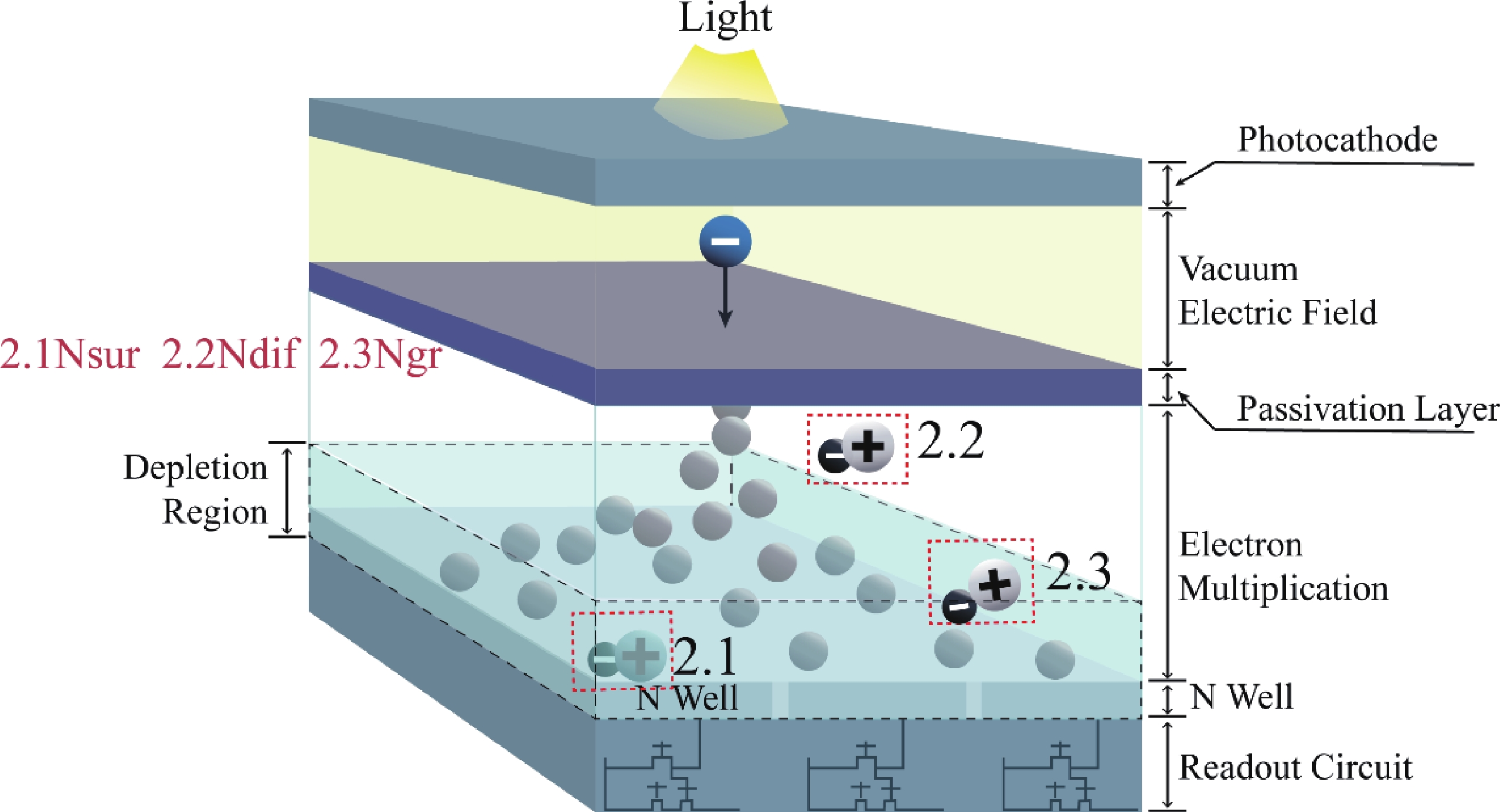
Fig. 1.
(Color online) Schematic diagram of noise generation mechanisms in the electron-bombarded complementary metal−oxide−semiconductor (EBCMOS) structure.
ARTICLES
Xinyue He1, Gangcheng Jiao2, Hongchang Cheng2, Tianjiao Lu1, Ye Li1, De Song1, and Weijun Chen1,
Corresponding author: De Song, songde614@163.com; Weijun Chen, weijun@cust.edu.cn
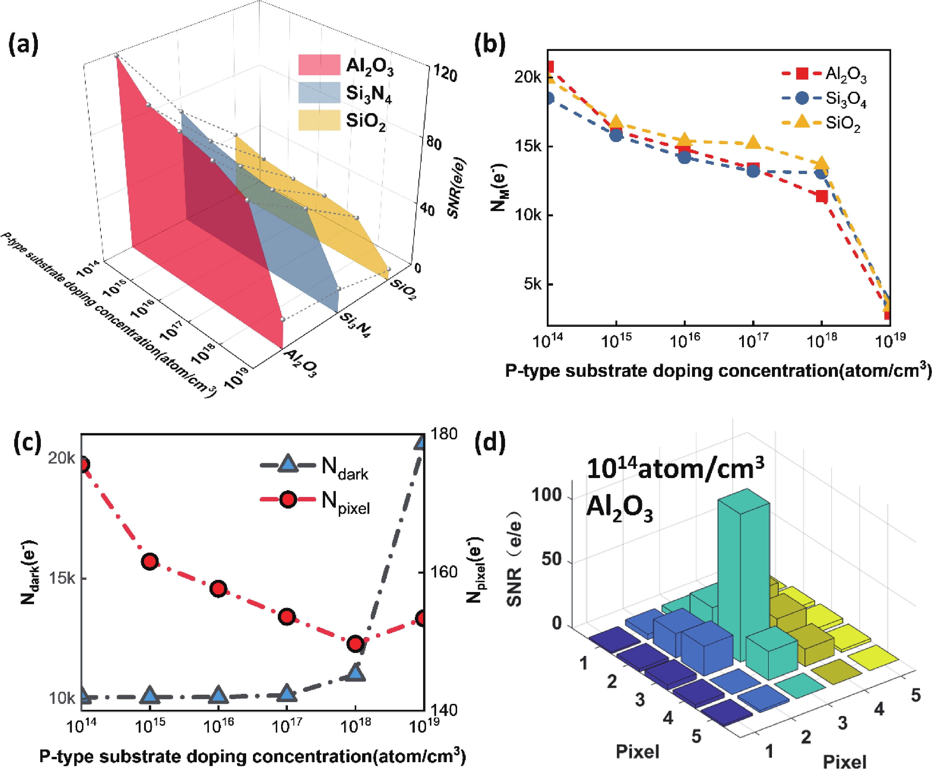
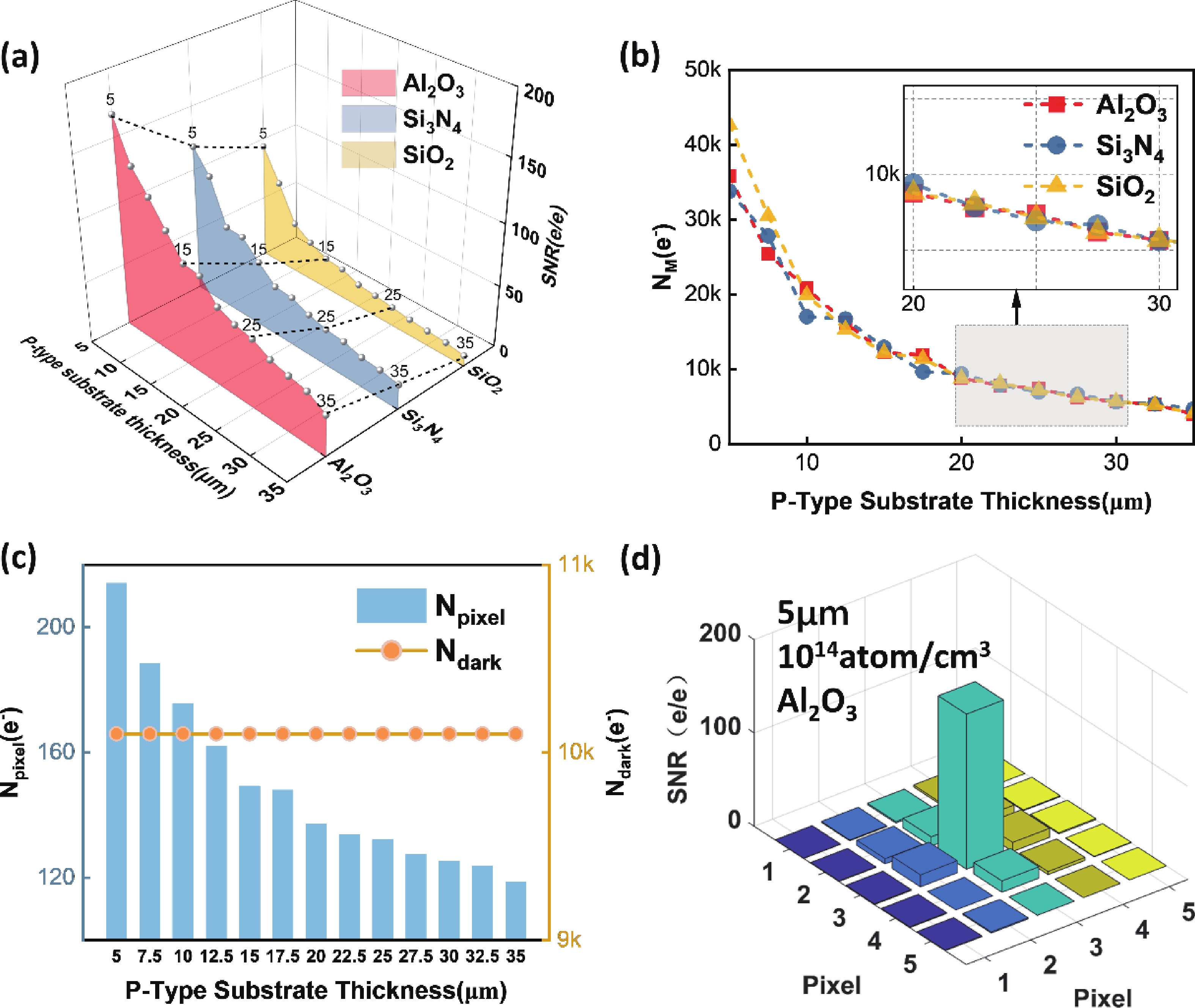
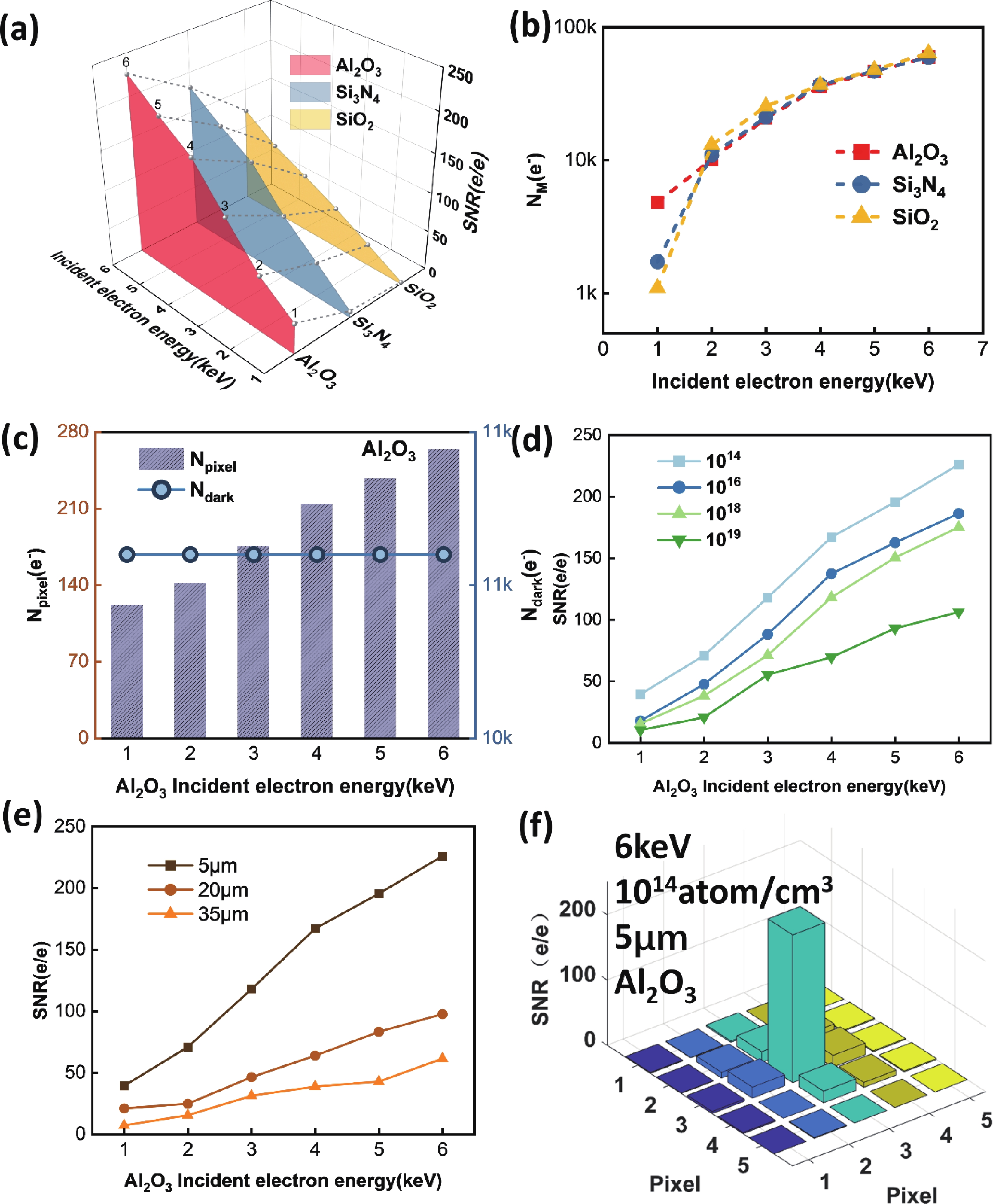
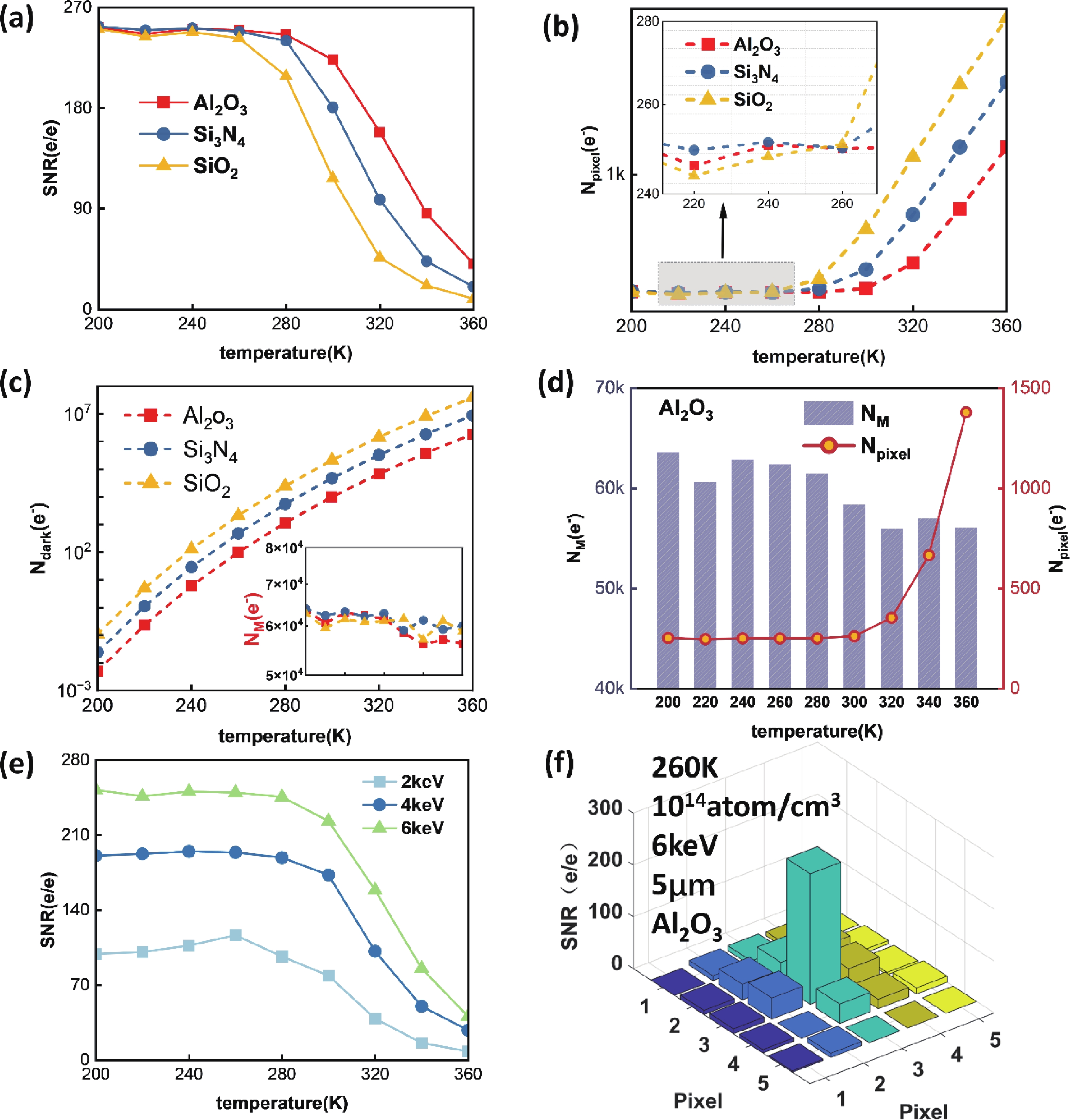
Abstract: In this study, with the aim of achieving a high signal-to-noise ratio (SNR) in an electron-bombarded complementary metal−oxide−semiconductor (EBCMOS) imaging chip, we analyzed the sources of noise using principles from low-light-level imaging and semiconductor theory, and established a physical computational model that relates the electron-multiplication layer to the noise characteristics of an EBCMOS chip in a uniformly doped structure with a P-type substrate. We conducted theoretical calculations to analyze the effects on noise characteristics of the passivation layer material and thickness, P-substrate doping concentration, P-substrate thickness, incident electron energy, and substrate temperature. By comparing the characteristics of pixel noise, dark current, multiplication electron numbers, and SNR under various structures, we simulated optimized structural parameters of the device. Our simulation results showed that the noise characteristics of the device could be optimized using an Al2O3 passivation thickness of 15 nm and substrate temperature of 260 K, and by decreasing the doping concentration and thickness of the P-type substrate and increasing the incident electron energy. The optimized SNR were 252 e/e. And the substantial impact of dark current noise, primarily governed by interfacial defects, on the overall noise characteristics of the device. This research offers theoretical support to develop EBCMOS imaging chips with high gain and SNR.
Keywords: EBCMOS, dark current electron number, gain, SNR
| [1] |
Aebi V, Costello K, Arcuni P, et al. EBAPS: Next generation, low power, digital night vision. OPTRO 2005 International Symposium, 2005: 1
|
| [2] |
Wang W, Li Y, Chen W J, et al. Simulation of the electrostatic distribution in the proximity focusing structure of an EBCMOS. IEEE Photonics J, 2020, 12(3): 6901210 doi: 10.1109/JPHOT.2020.2989095
|
| [3] |
Hirvonen L M, Jiggins S, Sergent N, et al. Photon counting imaging with an electron-bombarded CCD: Towards wide-field time-correlated single photon counting (TCSPC). Nucl Instrum Meth Phys Res Sect A Accel Spectrometers Detect Assoc Equip, 2015, 787: 323 doi: 10.1016/j.nima.2015.01.031
|
| [4] |
Jin W Q, Tao Y, Shi F, et al. Progress of low level light video technology. Infrared Laser Eng, 2015, 44(11): 3167 doi: 10.3969/j.issn.1007-2276.2015.11.001
|
| [5] |
Han J, Jiao G C, Yan L, et al. Research progress of digital low-light-level devices. J Appl Opt, 2023, 44(4): 874 doi: 10.5768/JAO202344.0406001
|
| [6] |
Bronzi D, Villa F, Tisa S, et al. SPAD figures of merit for photon-counting, photon-timing, and imaging applications: A review. IEEE Sens J, 2016, 16(1): 3 doi: 10.1109/JSEN.2015.2483565
|
| [7] |
Barbier R, Cajgfinger T, Calabria P, et al. A single-photon sensitive ebCMOS camera: The LUSIPHER prototype. Nucl Instrum Meth Phys Res Sect A Accel Spectrometers Detect Assoc Equip, 2011, 648(1): 266 doi: 10.1016/j.nima.2011.04.018
|
| [8] |
Barbier R, Depasse P, Baudot J, et al. First results from the development of a new generation of hybrid photon detector: EBCMOS. Astroparticle, particle and space physics, detectors and medical physics applications. 10th Conference Astroparticle, Particle and Space Physics, Detectors and Medical Physics Applications, 2007: 23 doi: 10.1142/9789812819093_0004
|
| [9] |
Aebi V W, Boyle J J. Electron bombarded active pixel sensor: EP1306906. 2011
|
| [10] |
Hirvonen L M, Suhling K. Photon counting imaging with an electron-bombarded pixel image sensor. Sensors, 2016, 16(5): 617 doi: 10.3390/s16050617
|
| [11] |
Cajgfinger T, Dominjon A, Barbier R. Single photon detection and localization accuracy with an ebCMOS camera. Nucl Instrum Meth Phys Res Sect A Accel Spectrometers Detect Assoc Equip, 2015, 787: 176 doi: 10.1016/j.nima.2014.11.090
|
| [12] |
Liu H L, Wang X, Tian J S, et al. High resolution electron bombareded complementary metal oxide semiconductor sensor for ultraviolet detection. Acta Phys Sin, 2018, 67(1): 175 doi: 10.7498/aps.67.20171729
|
| [13] |
Bai J Z, Bai Y L, Hou X, et al. The analysis of electron scattering among multiplying layer in EBAPS using optimized Monte Carlo method. Mod Phys Lett B, 2020, 34(34): 2050398 doi: 10.1142/S0217984920503984
|
| [14] |
Liu X, Li R Q, Jin W Q, et al. Total variational noise reduction method for EBAPS image based on weighted nuclear norm minimization. Opt Express, 2025, 33(2): 1932 doi: 10.1364/OE.546916
|
| [15] |
Yan Y Y, Qian Y S, Zhang J Z, et al. Design of spectral response test system for electron bombardment active pixel sensor. Laser Optoelectron Prog, 2022, 59(13): 1304001 doi: 10.3788/LOP202259.1304001
|
| [16] |
Li Q, Jin L X, Li G N. Research on fixed-mode noise correction of CMOS image sensor based on dark current. Chin J Liq Cryst Dis, 2021, 36(2): 327 doi: 10.37188/CJLCD.2020-0176
|
| [17] |
Li X, Hou Z X, Xu H Y, et al. Denoise method study on CMOS image sensor. Comput Eng Appl, 2011, 47(8): 167
|
| [18] |
Guo H L, Zhang R, Guo L J, et al. Preprocessing method of sensor pattern noise in camera source detection of photo images. Acta Photonica Sin, 2017, 46(6): 610003 doi: 10.3788/gzxb20174606.0610003
|
| [19] |
Guan J X, Li L, Zhang C, et al. Fixed pattern noise removal algorithm for CMOS image based on combined filter. Appl Laser, 2022, 42(4): 173 doi: 10.14128/j.cnki.al.20224204.173
|
| [20] |
Jiao G C, Song D, Yan Le, et al. Optimization simulation of charge collection efficiency of EBCMOS with substrate uniform and gradient doping. Chin J Lasers, 2024, 51(2): 0210001 doi: 10.3788/CJL230794
|
| [21] |
McGrath D, Tobin S, Goiffon V, et al. Dark current limiting mechanisms in CMOS image sensors. Ei, 2018, 30(11): 354 doi: 10.2352/ISSN.2470-1173.2018.11.IMSE-354
|
| [22] |
Yan L, shi F, cheng H C, et al. Research status of dark current in CMOS image sensor. Seventh Symposium on Novel Photoelectronic Detection Technology and Applications, 2021, 11763: 1085 doi: 10.1117/12.2586827
|
| [23] |
Yan L, Shi F, Cheng H C, et al. Study of dark current changes in alumina passivation film BCMOS sensors induced by low-energy electron bombardment. Infrared Techn, 2024, 46(3): 342
|
| [24] |
Zhang Y T, Cao K Q, Sun D X, et al. Low light level detection based on scientific CMOS image sensor with high sensitivity and low noise. Laser Optoelectron Prog, 2018, 55(8): 80401 doi: 10.3788/LOP55.080401
|
| [25] |
Song D, Shi F, Li Y. Simulation of charge collection efficiency for EBAPS with uniformly doped substrate. Infrared Laser Eng, 2016, 45(2): 203002 doi: 10.3788/m0001820164502.203002
|
| [26] |
Xu Z H. Simulation study on electron transport process of EBCMOS. Degree Dissertation, Changchun University of Science and Technology, 2022
|
| [27] |
Carrère J P, Place S, Oddou J P, et al. CMOS image sensor: Process impact on dark current. 2014 IEEE International Reliability Physics Symposium, 2014: 3C.1.1 doi: 10.1109/IRPS.2014.6860620
|
| [28] |
Lei R F, Wang Y, Gao J W, et al. Study on surface dark current of CCD. Electron Sci Technol, 2014, 27(5): 26 doi: 10.16180/j.cnki.issn1007-7820.2014.05.008
|
| [29] |
Werner F, Veith B, Zielke D, et al. Electronic and chemical properties of the c-Si/Al2O3 interface. J Appl Phys, 2011, 109(11): 113701 doi: 10.1063/1.3587227
|
| [30] |
Liu W J, Sayed I, Gupta C, et al. An improved methodology for extracting interface state density at Si3N4/GaN. Appl Phys Lett, 2020, 116(2): 022104 doi: 10.1063/1.5125645
|
| [31] |
Wang J M, Chen K J, Song J, et al. The fabrication and characterization of silicon-based ultra thin dielectric films. Res Prog SSE Solid State Electron, 2008, 28(1): 149
|
| [32] |
Song D, Zhou J Q, Mu Y N, et al. Testing system of multiplying electron gain for electron bombarded semiconductor. Fourth Seminar on Novel Optoelectronic Detection Technology and Application, 2018: 110 doi: 10.1117/12.2309747
|
| [33] |
Song Y Y, Song D, Li Y, et al. Influence of passivation layer and P-type base structure optimization on charge collection efficiency of electron bombardment active pixel sensor. Chin J Lasers, 2023, 50(18): 242 doi: 10.3788/CJL221159
|


Article views: 706 Times PDF downloads: 129 Times Cited by: 0 Times
Received: 25 March 2025 Revised: 26 June 2025 Online: Accepted Manuscript: 24 July 2025Uncorrected proof: 13 August 2025Published: 15 January 2026
| Citation: |
Xinyue He, Gangcheng Jiao, Hongchang Cheng, Tianjiao Lu, Ye Li, De Song, Weijun Chen. Influencing factors of noise characteristics in EBCMOS with uniformly doped P-type substrates[J]. Journal of Semiconductors, 2026, 47(1): 012302. doi: 10.1088/1674-4926/25030039
****
X Y He, G C Jiao, H C Cheng, T J Lu, Y Li, D Song, and W J Chen, Influencing factors of noise characteristics in EBCMOS with uniformly doped P-type substrates[J]. J. Semicond., 2026, 47(1): 012302 doi: 10.1088/1674-4926/25030039

|
 Xinyue He received her master’s degree in 2025 from Changchun University of Science and Technology, Changchun, Jilin, China, majoring in Electronic Science and Technology. Her current research interests include noise characteristics of Electron Bombarded CMOS (EBCMOS) devices and semiconductor thin-film imaging materials
 De Song received his doctoral degree from University of Chinese Academy of Sciences Changchun Institute of Applied Chemistry, Changchun, China, in 2009. He is currently an Associate Professor with the Changchun University of Science and Technology Changchun, Jilin, China. His current research interests include low-light-level imaging devices and systems
| [1] |
Aebi V, Costello K, Arcuni P, et al. EBAPS: Next generation, low power, digital night vision. OPTRO 2005 International Symposium, 2005: 1
|
| [2] |
Wang W, Li Y, Chen W J, et al. Simulation of the electrostatic distribution in the proximity focusing structure of an EBCMOS. IEEE Photonics J, 2020, 12(3): 6901210 doi: 10.1109/JPHOT.2020.2989095
|
| [3] |
Hirvonen L M, Jiggins S, Sergent N, et al. Photon counting imaging with an electron-bombarded CCD: Towards wide-field time-correlated single photon counting (TCSPC). Nucl Instrum Meth Phys Res Sect A Accel Spectrometers Detect Assoc Equip, 2015, 787: 323 doi: 10.1016/j.nima.2015.01.031
|
| [4] |
Jin W Q, Tao Y, Shi F, et al. Progress of low level light video technology. Infrared Laser Eng, 2015, 44(11): 3167 doi: 10.3969/j.issn.1007-2276.2015.11.001
|
| [5] |
Han J, Jiao G C, Yan L, et al. Research progress of digital low-light-level devices. J Appl Opt, 2023, 44(4): 874 doi: 10.5768/JAO202344.0406001
|
| [6] |
Bronzi D, Villa F, Tisa S, et al. SPAD figures of merit for photon-counting, photon-timing, and imaging applications: A review. IEEE Sens J, 2016, 16(1): 3 doi: 10.1109/JSEN.2015.2483565
|
| [7] |
Barbier R, Cajgfinger T, Calabria P, et al. A single-photon sensitive ebCMOS camera: The LUSIPHER prototype. Nucl Instrum Meth Phys Res Sect A Accel Spectrometers Detect Assoc Equip, 2011, 648(1): 266 doi: 10.1016/j.nima.2011.04.018
|
| [8] |
Barbier R, Depasse P, Baudot J, et al. First results from the development of a new generation of hybrid photon detector: EBCMOS. Astroparticle, particle and space physics, detectors and medical physics applications. 10th Conference Astroparticle, Particle and Space Physics, Detectors and Medical Physics Applications, 2007: 23 doi: 10.1142/9789812819093_0004
|
| [9] |
Aebi V W, Boyle J J. Electron bombarded active pixel sensor: EP1306906. 2011
|
| [10] |
Hirvonen L M, Suhling K. Photon counting imaging with an electron-bombarded pixel image sensor. Sensors, 2016, 16(5): 617 doi: 10.3390/s16050617
|
| [11] |
Cajgfinger T, Dominjon A, Barbier R. Single photon detection and localization accuracy with an ebCMOS camera. Nucl Instrum Meth Phys Res Sect A Accel Spectrometers Detect Assoc Equip, 2015, 787: 176 doi: 10.1016/j.nima.2014.11.090
|
| [12] |
Liu H L, Wang X, Tian J S, et al. High resolution electron bombareded complementary metal oxide semiconductor sensor for ultraviolet detection. Acta Phys Sin, 2018, 67(1): 175 doi: 10.7498/aps.67.20171729
|
| [13] |
Bai J Z, Bai Y L, Hou X, et al. The analysis of electron scattering among multiplying layer in EBAPS using optimized Monte Carlo method. Mod Phys Lett B, 2020, 34(34): 2050398 doi: 10.1142/S0217984920503984
|
| [14] |
Liu X, Li R Q, Jin W Q, et al. Total variational noise reduction method for EBAPS image based on weighted nuclear norm minimization. Opt Express, 2025, 33(2): 1932 doi: 10.1364/OE.546916
|
| [15] |
Yan Y Y, Qian Y S, Zhang J Z, et al. Design of spectral response test system for electron bombardment active pixel sensor. Laser Optoelectron Prog, 2022, 59(13): 1304001 doi: 10.3788/LOP202259.1304001
|
| [16] |
Li Q, Jin L X, Li G N. Research on fixed-mode noise correction of CMOS image sensor based on dark current. Chin J Liq Cryst Dis, 2021, 36(2): 327 doi: 10.37188/CJLCD.2020-0176
|
| [17] |
Li X, Hou Z X, Xu H Y, et al. Denoise method study on CMOS image sensor. Comput Eng Appl, 2011, 47(8): 167
|
| [18] |
Guo H L, Zhang R, Guo L J, et al. Preprocessing method of sensor pattern noise in camera source detection of photo images. Acta Photonica Sin, 2017, 46(6): 610003 doi: 10.3788/gzxb20174606.0610003
|
| [19] |
Guan J X, Li L, Zhang C, et al. Fixed pattern noise removal algorithm for CMOS image based on combined filter. Appl Laser, 2022, 42(4): 173 doi: 10.14128/j.cnki.al.20224204.173
|
| [20] |
Jiao G C, Song D, Yan Le, et al. Optimization simulation of charge collection efficiency of EBCMOS with substrate uniform and gradient doping. Chin J Lasers, 2024, 51(2): 0210001 doi: 10.3788/CJL230794
|
| [21] |
McGrath D, Tobin S, Goiffon V, et al. Dark current limiting mechanisms in CMOS image sensors. Ei, 2018, 30(11): 354 doi: 10.2352/ISSN.2470-1173.2018.11.IMSE-354
|
| [22] |
Yan L, shi F, cheng H C, et al. Research status of dark current in CMOS image sensor. Seventh Symposium on Novel Photoelectronic Detection Technology and Applications, 2021, 11763: 1085 doi: 10.1117/12.2586827
|
| [23] |
Yan L, Shi F, Cheng H C, et al. Study of dark current changes in alumina passivation film BCMOS sensors induced by low-energy electron bombardment. Infrared Techn, 2024, 46(3): 342
|
| [24] |
Zhang Y T, Cao K Q, Sun D X, et al. Low light level detection based on scientific CMOS image sensor with high sensitivity and low noise. Laser Optoelectron Prog, 2018, 55(8): 80401 doi: 10.3788/LOP55.080401
|
| [25] |
Song D, Shi F, Li Y. Simulation of charge collection efficiency for EBAPS with uniformly doped substrate. Infrared Laser Eng, 2016, 45(2): 203002 doi: 10.3788/m0001820164502.203002
|
| [26] |
Xu Z H. Simulation study on electron transport process of EBCMOS. Degree Dissertation, Changchun University of Science and Technology, 2022
|
| [27] |
Carrère J P, Place S, Oddou J P, et al. CMOS image sensor: Process impact on dark current. 2014 IEEE International Reliability Physics Symposium, 2014: 3C.1.1 doi: 10.1109/IRPS.2014.6860620
|
| [28] |
Lei R F, Wang Y, Gao J W, et al. Study on surface dark current of CCD. Electron Sci Technol, 2014, 27(5): 26 doi: 10.16180/j.cnki.issn1007-7820.2014.05.008
|
| [29] |
Werner F, Veith B, Zielke D, et al. Electronic and chemical properties of the c-Si/Al2O3 interface. J Appl Phys, 2011, 109(11): 113701 doi: 10.1063/1.3587227
|
| [30] |
Liu W J, Sayed I, Gupta C, et al. An improved methodology for extracting interface state density at Si3N4/GaN. Appl Phys Lett, 2020, 116(2): 022104 doi: 10.1063/1.5125645
|
| [31] |
Wang J M, Chen K J, Song J, et al. The fabrication and characterization of silicon-based ultra thin dielectric films. Res Prog SSE Solid State Electron, 2008, 28(1): 149
|
| [32] |
Song D, Zhou J Q, Mu Y N, et al. Testing system of multiplying electron gain for electron bombarded semiconductor. Fourth Seminar on Novel Optoelectronic Detection Technology and Application, 2018: 110 doi: 10.1117/12.2309747
|
| [33] |
Song Y Y, Song D, Li Y, et al. Influence of passivation layer and P-type base structure optimization on charge collection efficiency of electron bombardment active pixel sensor. Chin J Lasers, 2023, 50(18): 242 doi: 10.3788/CJL221159
|

 WeChat ID
Journal of Semiconductors © 2017 All Rights Reserved 京ICP备05085259号-2

 DownLoad:

