


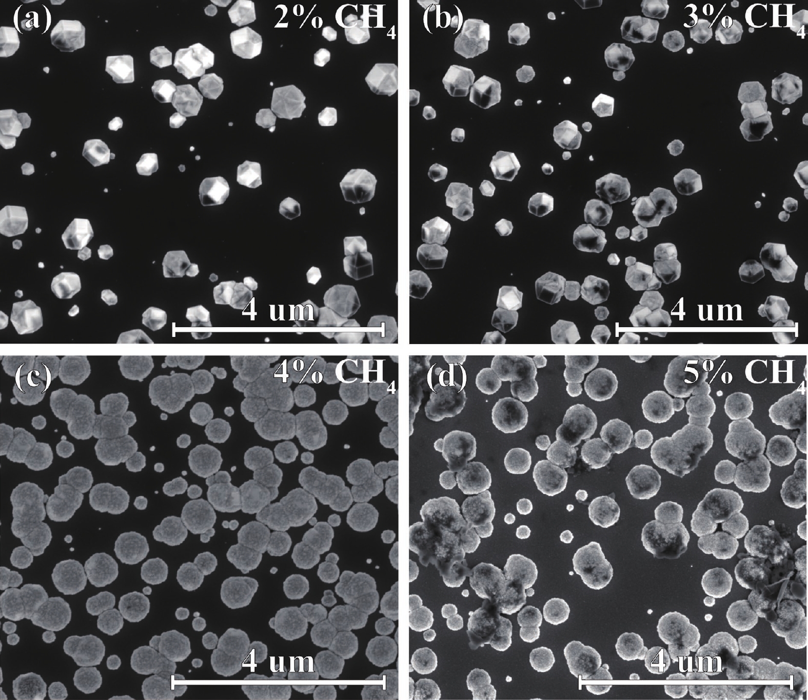
Fig. 1.
The SEM results of the diamond growth for 1 h under different methane-hydrogen flow ratios. (a) 2%; (b) 3%; (c) 4%; and (d) 5%.
ARTICLES
Pengfei Qu1, §, Guangdi Zhou1, §, Peng Jin1, 2, , Xu Han1 and Zhanguo Wang1, 2
Corresponding author: Peng Jin, pengjin@semi.ac.cn
Abstract: The synthesis of high-quality heteroepitaxial diamond films on iridium composite substrates is a critical step toward advancing diamond for electronic and optical applications. Microwave plasma chemical vapor deposition, combined with in situ optical emission spectroscopy, enables precise control over growth modes through plasma parameter tuning. In this study, we examine how methane concentration, microwave power, and gas pressure influence plasma species and, consequently, the growth modes of heteroepitaxial diamond by optical emission spectroscopy and scanning electron microscope. At low nucleation densities, increased methane concentrations promote the transition from faceted polyhedral to ballas structures, driven by elevated C2 radical concentrations in the plasma. Conversely, at higher nucleation densities, gas pressure, and substrate temperature dominate growth mode determination, leading to diverse morphologies, such as planar, polycrystalline, octahedral, and step-flow growth. These findings elucidate the interplay among plasma species, growth parameters, and growth mode, offering critical insights for optimizing growth conditions and preparing heteroepitaxial diamond films in a specific growth mode.
Keywords: heteroepitaxy, diamond films, growth modes, MPCVD, OES
| [1] |
Wort C J H, Balmer R S. Diamond as an electronic material. Mater Today, 2008, 11(1): 22 doi: 10.1016/S1369-7021(07)70349-8
|
| [2] |
Geis M W, Wade T C, Wuorio C H, et al. Progress toward diamond power field-effect transistors. Phys Status Solidi A, 2018, 215(22): 1800681 doi: 10.1002/pssa.201800681
|
| [3] |
Kwak T, Nam Y, Kwon Y, et al. Depletion-mode and enhancement-mode diamond MOSFETs fabricated on the same heteroepitaxial diamond substrates. Diam Relat Mater, 2025, 153: 112022 doi: 10.1016/j.diamond.2025.112022
|
| [4] |
Kwak T, Lee J, Choi U, et al. Diamond schottky barrier diodes fabricated on sapphire-based freestanding heteroepitaxial diamond substrate. Diam Relat Mater, 2021, 114: 108335 doi: 10.1016/j.diamond.2021.108335
|
| [5] |
Feng M, Jin P, Meng X, et al. Performance of metal-semiconductor-metal structured diamond deep-ultraviolet photodetector with a large active area. J Phys D: Appl Phys, 2022, 55(40): 404005 doi: 10.1088/1361-6463/ac83ce
|
| [6] |
Zhang X, Matsumoto T, Nakano Y, et al. Inversion channel MOSFET on heteroepitaxially grown free-standing diamond. Carbon, 2021, 175: 615 doi: 10.1016/j.carbon.2020.11.072
|
| [7] |
Uwihoreye V, Hu Y, Cao G, et al. Recent progress on heteroepitaxial growth of single crystal diamond films. Electron, 2024, 2(4): e70 doi: 10.1002/elt2.70
|
| [8] |
Schreck M, Gsell S, Brescia R, et al. Ion bombardment induced buried lateral growth, the key mechanism for the synthesis of single crystal diamond wafers. Sci Rep, 2017, 7(1): 44462 doi: 10.1038/srep44462
|
| [9] |
Kim S W, Takaya R, Hirano S, et al. Two-inch high-quality (001) diamond heteroepitaxial growth on sapphire (11-20) misoriented substrate by step-flow mode. Appl Phys Express, 2021, 14(11): 115501 doi: 10.35848/1882-0786/ac28e7
|
| [10] |
Kim S W, Kawamata Y, Takaya R, et al. Growth of high-quality one-inch free-standing heteroepitaxial (001) diamond on (11-20) sapphire substrate. Appl Phys Lett, 2020, 117(20): 202102 doi: 10.1063/5.0024070
|
| [11] |
Qu P, Jin P, Zhou G, et al. Growth of two-inch free-standing heteroepitaxial diamond on Ir/YSZ/Si (001) substrates via laser-patterned templates. J Semicond, 2024, 45(9): 090501 doi: 10.1088/1674-4926/24060003
|
| [12] |
Aida H, Ihara T, Oshima R, et al. Analysis of external surface and internal lattice curvatures of freestanding heteroepitaxial diamond grown on an Ir (001)/MgO (001) substrate. Diam Relat Mater, 2023, 136: 110026 doi: 10.1016/j.diamond.2023.110026
|
| [13] |
Kasu M, Takaya R, Kim S W. Growth of high-quality inch-diameter heteroepitaxial diamond layers on sapphire substrates in comparison to MgO substrates. Diam Relat Mater, 2022, 126: 109086 doi: 10.1016/j.diamond.2022.109086
|
| [14] |
Schreck M, Peter T. Wafer bow in diamond heteroepitaxy: Causes, their analytical description, and viable solutions. J Appl Phys, 2025, 137(1): 015108 doi: 10.1063/5.0245362
|
| [15] |
Aida H, Kim S W, Ikejiri K, et al. Fabrication of freestanding heteroepitaxial diamond substrate via micropatterns and microneedles. Appl Phys Express, 2016, 9(3): 035504 doi: 10.7567/APEX.9.035504
|
| [16] |
Ichikawa K, Kurone K, Kodama H, et al. High crystalline quality heteroepitaxial diamond using grid-patterned nucleation and growth on ir. Diam Relat Mater, 2019, 94: 92 doi: 10.1016/j.diamond.2019.01.027
|
| [17] |
Tang Y H, Golding B. Stress engineering of high-quality single crystal diamond by heteroepitaxial lateral overgrowth. Appl Phys Lett, 2016, 108(5): 052101 doi: 10.1063/1.4941291
|
| [18] |
Mehmel L, Issaoui R, Brinza O, et al. Dislocation density reduction using overgrowth on hole arrays made in heteroepitaxial diamond substrates. Appl Phys Lett, 2021, 118(6): 061901 doi: 10.1063/5.0033741
|
| [19] |
Tallaire A, Achard J, Silva F, et al. Homoepitaxial deposition of high-quality thick diamond films: Effect of growth parameters. Diam Relat Mater, 2005, 14(3): 249 doi: 10.1016/j.diamond.2004.10.037
|
| [20] |
Achard J, Silva F, Tallaire A, et al. High quality MPACVD diamond single crystal growth: High microwave power density regime. J Phys D: Appl Phys, 2007, 40(20): 6175 doi: 10.1088/0022-3727/40/20/S04
|
| [21] |
Muchnikov A B, Vikharev A L, Gorbachev A M, et al. Homoepitaxial single crystal diamond growth at different gas pressures and MPACVD reactor configurations. Diam Relat Mater, 2010, 19(5): 432 doi: 10.1016/j.diamond.2009.11.01224
|
| [22] |
Yu Z, Flodstr A. Pressure dependence of growth mode of HFCVD diamond. Diam. Relat Mater, 1997, 6: 81 doi: 10.1016/S0925-9635(96)00742-X
|
| [23] |
Lai W C, Wu Y S, Chang H C, et al. Differing morphologies of textured diamond films with electrical properties made with microwave plasma chemical vapor deposition. Appl Surf Sci, 2010, 257(5): 1729 doi: 10.1016/j.apsusc.2010.09.006
|
| [24] |
Van der Drift A. Evolutionary selection, a principle governing growth orientation in vapour-deposited layers. Philips Res Rep, 1967, 22(3): 267
|
| [25] |
Wild C, Kohl R, Herres N, et al. Oriented CVD diamond films: twin formation, structure and morphology. Diam Relat Mater, 1994, 3(4): 373 doi: 10.1016/0925-9635(94)90188-0
|
| [26] |
Hemawan K W, Hemley R J. Optical emission diagnostics of plasmas in chemical vapor deposition of single-crystal diamond. J Vac Sci Technol, A, 2015, 33(6): 061302 doi: 10.1116/1.4928031
|
| [27] |
Gong Y, Jia W, Zhou B, et al. Heavily boron-doped polycrystalline diamond films: Microstructure, chemical composition investigation and plasma in-situ diagnostics. Appl Surf Sci, 2024, 659: 159838 doi: 10.1016/j.apsusc.2024.159838
|
| [28] |
Shimaoka T, Yamada H, Mokuno Y, et al. Oxygen concentration dependence in microwave plasma-enhanced chemical vapor deposition diamond growth in the (H, C, O, N) system. Phys Status Solidi A, 2022, 219(11): 2100887 doi: 10.1002/pssa.202100887
|
| [29] |
Bogdanov S A, Gorbachev A M, Vikharev A L, et al. Study of microwave discharge at high power density conditions in diamond chemical vapor deposition reactor by optical emission spectroscopy. Diam Relat Mater, 2019, 97: 107407 doi: 10.1016/j.diamond.2019.04.030
|
| [30] |
Qu P, Jin P, Zhou G, et al. Epitaxial growth of high-quality yttria-stabilized zirconia films with uniform thickness on silicon by the combination of PLD and RF sputtering. Surf Coat Technol, 2023, 456: 129267 doi: 10.1016/j.surfcoat.2023.129267
|
| [31] |
Zhou G, Qu P, Huo X, et al. The deposition of Ir/YSZ double-layer thin films on silicon by PLD and magnetron sputtering: Growth kinetics and the effects of oxygen. Results Phys, 2023, 47: 106357 doi: 10.1016/j.rinp.2023.106357
|
| [32] |
May P W, Ashfold M N R, Mankelevich Yu A. Microcrystalline, nanocrystalline, and ultrananocrystalline diamond chemical vapor deposition: Experiment and modeling of the factors controlling growth rate, nucleation, and crystal size. J Appl Phys, 2007, 101(5): 053115 doi: 10.1063/1.2696363
|
| [33] |
Ashkinazi E, Khmelnitskii R, Sedov V, et al. Morphology of diamond layers grown on different facets of single crystal diamond substrates by a microwave plasma CVD in CH4-H2-N2 gas mixtures. Crystals, 2017, 7(6): 166 doi: 10.3390/cryst7060166
|
| [34] |
Sharma R, Woehrl N, Vrućinić M, et al. Effect of microwave power and C2 emission intensity on structural and surface properties of nanocrystalline diamond films. Thin Solid Films, 2011, 519(22): 7632 doi: 10.1016/j.tsf.2011.05.006
|
| [35] |
Macdonald A D. High frequency gas discharge breakdown in hydrogen. Phys Rev, 1949, 76(11): 1634 doi: 10.1103/PhysRev.76.1634
|
| [36] |
Shivkumar G, Tholeti S S, Alrefae M A, et al. Analysis of hydrogen plasma in a microwave plasma chemical vapor deposition reactor. J Appl Phys, 2016, 119(11): 113301 doi: 10.1063/1.4943025
|
| [37] |
Redfern P C, Horner D A, Curtiss L A, et al. Theoretical studies of growth of diamond (110) from dicarbon. J Phys Chem, 1996, 100(28): 11654 doi: 10.1021/jp953165g
|
| [38] |
Shao G, Wang J, Zhang S, et al. Surface morphology and microstructure evolution of single crystal diamond during different homoepitaxial growth stages. Materials, 2021, 14(20): 5964 doi: 10.3390/ma14205964
|
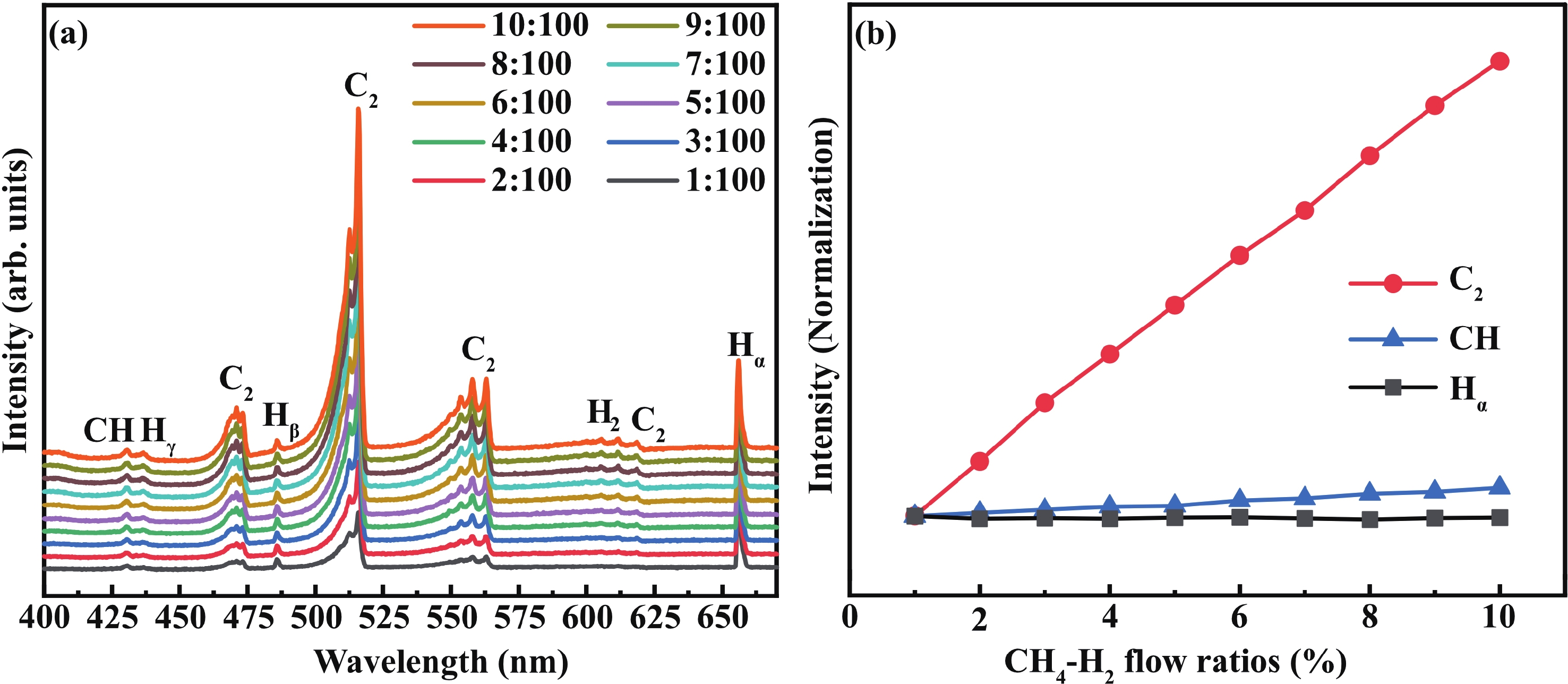
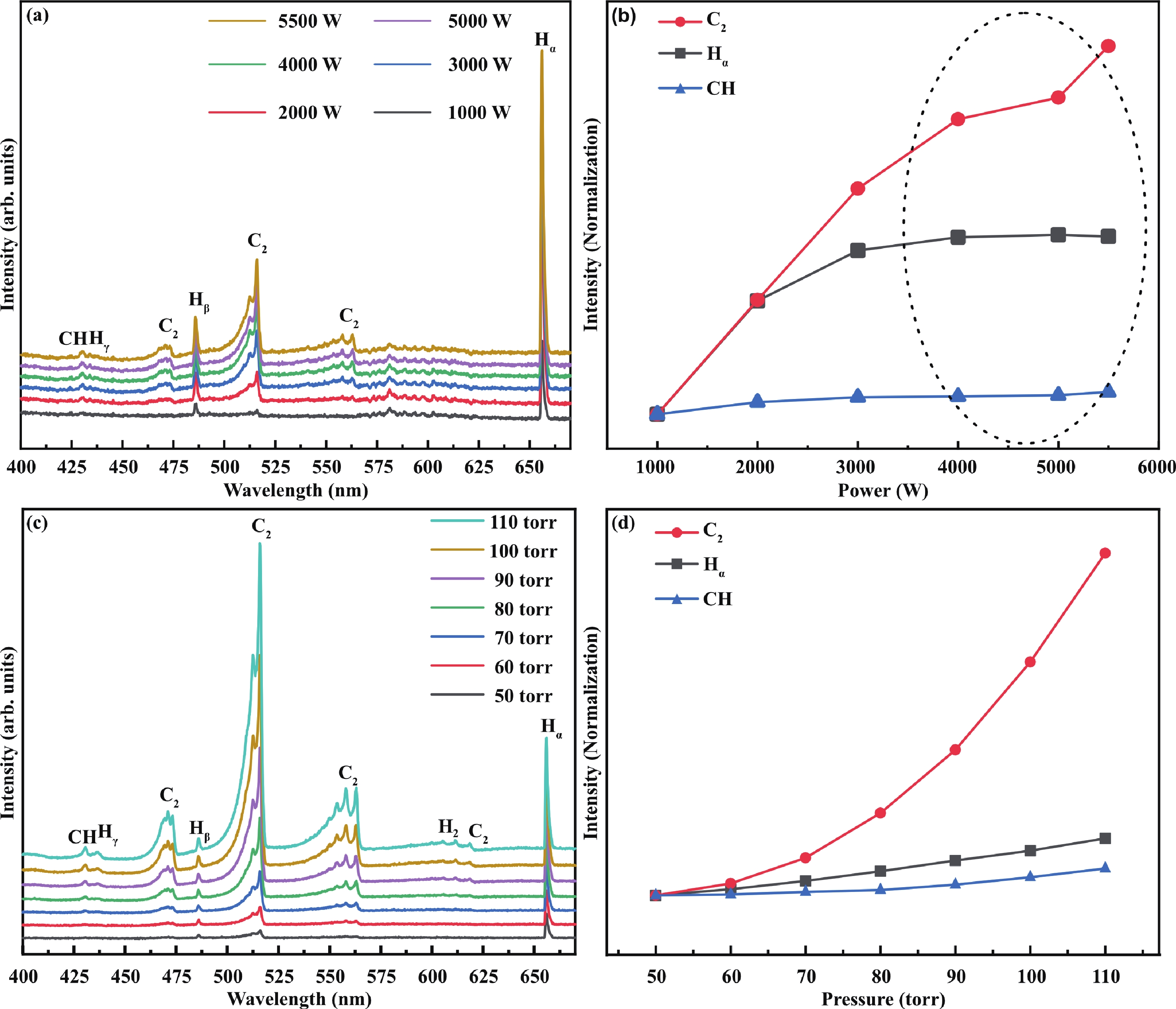
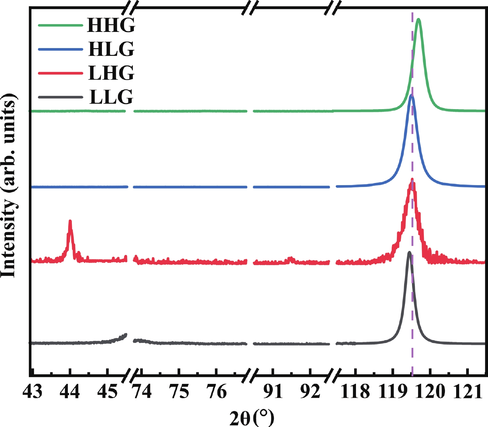
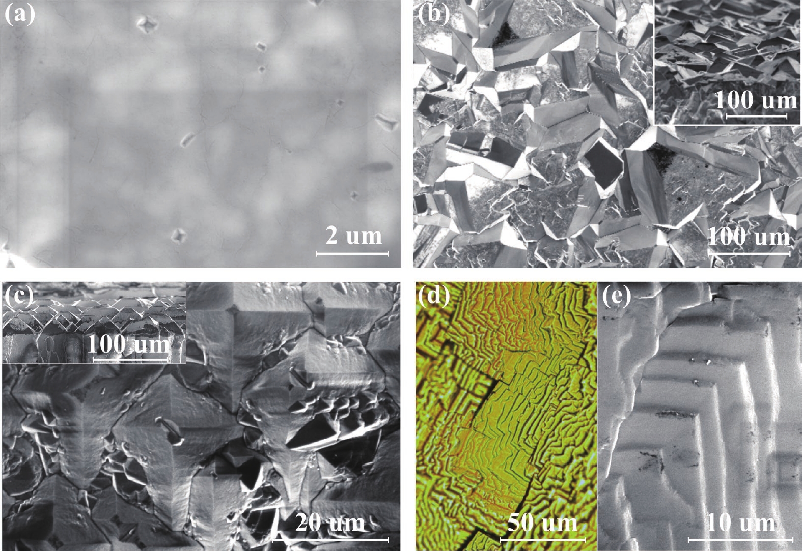
Table 1. Growth parameters of the samples.
| Samples | Growth regimes |
MW power (W) |
Pressure (Torr) |
CH4 concentration (%) |
Substrate temperature (°C) |
BEN duration (min) |
Growth duration (h) |
| A1 | − | 5000 | 50 | 2 | 850 | 30 | 1 |
| A2 | − | 5000 | 50 | 3 | 850 | 30 | 1 |
| A3 | − | 5000 | 50 | 4 | 850 | 30 | 1 |
| A4 | − | 5000 | 50 | 5 | 850 | 30 | 1 |
| B1 | LLG | 5000 | 50 | 2 | 850 | 60 | 12 |
| B2 | LHG | 5000 | 50 | 2 | 1050 | 60 | 12 |
| B3 | HLG | 5000 | 120 | 2 | 850 | 60 | 12 |
| B4 | HHG | 5000 | 134 | 2 | 1050 | 60 | 12 |
 DownLoad: CSV
| [1] |
Wort C J H, Balmer R S. Diamond as an electronic material. Mater Today, 2008, 11(1): 22 doi: 10.1016/S1369-7021(07)70349-8
|
| [2] |
Geis M W, Wade T C, Wuorio C H, et al. Progress toward diamond power field-effect transistors. Phys Status Solidi A, 2018, 215(22): 1800681 doi: 10.1002/pssa.201800681
|
| [3] |
Kwak T, Nam Y, Kwon Y, et al. Depletion-mode and enhancement-mode diamond MOSFETs fabricated on the same heteroepitaxial diamond substrates. Diam Relat Mater, 2025, 153: 112022 doi: 10.1016/j.diamond.2025.112022
|
| [4] |
Kwak T, Lee J, Choi U, et al. Diamond schottky barrier diodes fabricated on sapphire-based freestanding heteroepitaxial diamond substrate. Diam Relat Mater, 2021, 114: 108335 doi: 10.1016/j.diamond.2021.108335
|
| [5] |
Feng M, Jin P, Meng X, et al. Performance of metal-semiconductor-metal structured diamond deep-ultraviolet photodetector with a large active area. J Phys D: Appl Phys, 2022, 55(40): 404005 doi: 10.1088/1361-6463/ac83ce
|
| [6] |
Zhang X, Matsumoto T, Nakano Y, et al. Inversion channel MOSFET on heteroepitaxially grown free-standing diamond. Carbon, 2021, 175: 615 doi: 10.1016/j.carbon.2020.11.072
|
| [7] |
Uwihoreye V, Hu Y, Cao G, et al. Recent progress on heteroepitaxial growth of single crystal diamond films. Electron, 2024, 2(4): e70 doi: 10.1002/elt2.70
|
| [8] |
Schreck M, Gsell S, Brescia R, et al. Ion bombardment induced buried lateral growth, the key mechanism for the synthesis of single crystal diamond wafers. Sci Rep, 2017, 7(1): 44462 doi: 10.1038/srep44462
|
| [9] |
Kim S W, Takaya R, Hirano S, et al. Two-inch high-quality (001) diamond heteroepitaxial growth on sapphire (11-20) misoriented substrate by step-flow mode. Appl Phys Express, 2021, 14(11): 115501 doi: 10.35848/1882-0786/ac28e7
|
| [10] |
Kim S W, Kawamata Y, Takaya R, et al. Growth of high-quality one-inch free-standing heteroepitaxial (001) diamond on (11-20) sapphire substrate. Appl Phys Lett, 2020, 117(20): 202102 doi: 10.1063/5.0024070
|
| [11] |
Qu P, Jin P, Zhou G, et al. Growth of two-inch free-standing heteroepitaxial diamond on Ir/YSZ/Si (001) substrates via laser-patterned templates. J Semicond, 2024, 45(9): 090501 doi: 10.1088/1674-4926/24060003
|
| [12] |
Aida H, Ihara T, Oshima R, et al. Analysis of external surface and internal lattice curvatures of freestanding heteroepitaxial diamond grown on an Ir (001)/MgO (001) substrate. Diam Relat Mater, 2023, 136: 110026 doi: 10.1016/j.diamond.2023.110026
|
| [13] |
Kasu M, Takaya R, Kim S W. Growth of high-quality inch-diameter heteroepitaxial diamond layers on sapphire substrates in comparison to MgO substrates. Diam Relat Mater, 2022, 126: 109086 doi: 10.1016/j.diamond.2022.109086
|
| [14] |
Schreck M, Peter T. Wafer bow in diamond heteroepitaxy: Causes, their analytical description, and viable solutions. J Appl Phys, 2025, 137(1): 015108 doi: 10.1063/5.0245362
|
| [15] |
Aida H, Kim S W, Ikejiri K, et al. Fabrication of freestanding heteroepitaxial diamond substrate via micropatterns and microneedles. Appl Phys Express, 2016, 9(3): 035504 doi: 10.7567/APEX.9.035504
|
| [16] |
Ichikawa K, Kurone K, Kodama H, et al. High crystalline quality heteroepitaxial diamond using grid-patterned nucleation and growth on ir. Diam Relat Mater, 2019, 94: 92 doi: 10.1016/j.diamond.2019.01.027
|
| [17] |
Tang Y H, Golding B. Stress engineering of high-quality single crystal diamond by heteroepitaxial lateral overgrowth. Appl Phys Lett, 2016, 108(5): 052101 doi: 10.1063/1.4941291
|
| [18] |
Mehmel L, Issaoui R, Brinza O, et al. Dislocation density reduction using overgrowth on hole arrays made in heteroepitaxial diamond substrates. Appl Phys Lett, 2021, 118(6): 061901 doi: 10.1063/5.0033741
|
| [19] |
Tallaire A, Achard J, Silva F, et al. Homoepitaxial deposition of high-quality thick diamond films: Effect of growth parameters. Diam Relat Mater, 2005, 14(3): 249 doi: 10.1016/j.diamond.2004.10.037
|
| [20] |
Achard J, Silva F, Tallaire A, et al. High quality MPACVD diamond single crystal growth: High microwave power density regime. J Phys D: Appl Phys, 2007, 40(20): 6175 doi: 10.1088/0022-3727/40/20/S04
|
| [21] |
Muchnikov A B, Vikharev A L, Gorbachev A M, et al. Homoepitaxial single crystal diamond growth at different gas pressures and MPACVD reactor configurations. Diam Relat Mater, 2010, 19(5): 432 doi: 10.1016/j.diamond.2009.11.01224
|
| [22] |
Yu Z, Flodstr A. Pressure dependence of growth mode of HFCVD diamond. Diam. Relat Mater, 1997, 6: 81 doi: 10.1016/S0925-9635(96)00742-X
|
| [23] |
Lai W C, Wu Y S, Chang H C, et al. Differing morphologies of textured diamond films with electrical properties made with microwave plasma chemical vapor deposition. Appl Surf Sci, 2010, 257(5): 1729 doi: 10.1016/j.apsusc.2010.09.006
|
| [24] |
Van der Drift A. Evolutionary selection, a principle governing growth orientation in vapour-deposited layers. Philips Res Rep, 1967, 22(3): 267
|
| [25] |
Wild C, Kohl R, Herres N, et al. Oriented CVD diamond films: twin formation, structure and morphology. Diam Relat Mater, 1994, 3(4): 373 doi: 10.1016/0925-9635(94)90188-0
|
| [26] |
Hemawan K W, Hemley R J. Optical emission diagnostics of plasmas in chemical vapor deposition of single-crystal diamond. J Vac Sci Technol, A, 2015, 33(6): 061302 doi: 10.1116/1.4928031
|
| [27] |
Gong Y, Jia W, Zhou B, et al. Heavily boron-doped polycrystalline diamond films: Microstructure, chemical composition investigation and plasma in-situ diagnostics. Appl Surf Sci, 2024, 659: 159838 doi: 10.1016/j.apsusc.2024.159838
|
| [28] |
Shimaoka T, Yamada H, Mokuno Y, et al. Oxygen concentration dependence in microwave plasma-enhanced chemical vapor deposition diamond growth in the (H, C, O, N) system. Phys Status Solidi A, 2022, 219(11): 2100887 doi: 10.1002/pssa.202100887
|
| [29] |
Bogdanov S A, Gorbachev A M, Vikharev A L, et al. Study of microwave discharge at high power density conditions in diamond chemical vapor deposition reactor by optical emission spectroscopy. Diam Relat Mater, 2019, 97: 107407 doi: 10.1016/j.diamond.2019.04.030
|
| [30] |
Qu P, Jin P, Zhou G, et al. Epitaxial growth of high-quality yttria-stabilized zirconia films with uniform thickness on silicon by the combination of PLD and RF sputtering. Surf Coat Technol, 2023, 456: 129267 doi: 10.1016/j.surfcoat.2023.129267
|
| [31] |
Zhou G, Qu P, Huo X, et al. The deposition of Ir/YSZ double-layer thin films on silicon by PLD and magnetron sputtering: Growth kinetics and the effects of oxygen. Results Phys, 2023, 47: 106357 doi: 10.1016/j.rinp.2023.106357
|
| [32] |
May P W, Ashfold M N R, Mankelevich Yu A. Microcrystalline, nanocrystalline, and ultrananocrystalline diamond chemical vapor deposition: Experiment and modeling of the factors controlling growth rate, nucleation, and crystal size. J Appl Phys, 2007, 101(5): 053115 doi: 10.1063/1.2696363
|
| [33] |
Ashkinazi E, Khmelnitskii R, Sedov V, et al. Morphology of diamond layers grown on different facets of single crystal diamond substrates by a microwave plasma CVD in CH4-H2-N2 gas mixtures. Crystals, 2017, 7(6): 166 doi: 10.3390/cryst7060166
|
| [34] |
Sharma R, Woehrl N, Vrućinić M, et al. Effect of microwave power and C2 emission intensity on structural and surface properties of nanocrystalline diamond films. Thin Solid Films, 2011, 519(22): 7632 doi: 10.1016/j.tsf.2011.05.006
|
| [35] |
Macdonald A D. High frequency gas discharge breakdown in hydrogen. Phys Rev, 1949, 76(11): 1634 doi: 10.1103/PhysRev.76.1634
|
| [36] |
Shivkumar G, Tholeti S S, Alrefae M A, et al. Analysis of hydrogen plasma in a microwave plasma chemical vapor deposition reactor. J Appl Phys, 2016, 119(11): 113301 doi: 10.1063/1.4943025
|
| [37] |
Redfern P C, Horner D A, Curtiss L A, et al. Theoretical studies of growth of diamond (110) from dicarbon. J Phys Chem, 1996, 100(28): 11654 doi: 10.1021/jp953165g
|
| [38] |
Shao G, Wang J, Zhang S, et al. Surface morphology and microstructure evolution of single crystal diamond during different homoepitaxial growth stages. Materials, 2021, 14(20): 5964 doi: 10.3390/ma14205964
|


Article views: 1092 Times PDF downloads: 116 Times Cited by: 0 Times
Received: 03 November 2025 Revised: 19 November 2025 Online: Accepted Manuscript: 15 December 2025Uncorrected proof: 17 December 2025Published: 15 January 2026
| Citation: |
Pengfei Qu, Guangdi Zhou, Peng Jin, Xu Han, Zhanguo Wang. Evolution of diamond film growth modes under varied plasma conditions: insights from optical emission spectroscopy[J]. Journal of Semiconductors, 2026, 47(1): 012502. doi: 10.1088/1674-4926/25110003
****
P F Qu, G D Zhou, P Jin, X Han, and Z G Wang, Evolution of diamond film growth modes under varied plasma conditions: insights from optical emission spectroscopy[J]. J. Semicond., 2026, 47(1): 012502 doi: 10.1088/1674-4926/25110003

|
 Pengfei Qu got his B.S. degree from Jilin University, Changchun, China, in 2019, and the Ph.D. degree from Institute of Semiconductors, CAS, Beijing, China, in 2024. He is currently pursuing postdoctoral research at the Institute of Semiconductors, CAS. His research interests mainly focus on materials and devices of heteroepitaxial single-crystal diamond
 Peng Jin got his BS and PhD from Nankai University in 1996 and 2001, respectively. He did postdoctoral research at Institute of Semiconductors, CAS. In 2003, he joined Institute of Semiconductors, CAS as an associate professor. In 2009, he was promoted to be a professor. In 2015, he became a professor of UCAS. The current research focuses on semiconductor diamond materials and devices, low dimensional semiconductor materials and devices, scientific instruments, etc
| [1] |
Wort C J H, Balmer R S. Diamond as an electronic material. Mater Today, 2008, 11(1): 22 doi: 10.1016/S1369-7021(07)70349-8
|
| [2] |
Geis M W, Wade T C, Wuorio C H, et al. Progress toward diamond power field-effect transistors. Phys Status Solidi A, 2018, 215(22): 1800681 doi: 10.1002/pssa.201800681
|
| [3] |
Kwak T, Nam Y, Kwon Y, et al. Depletion-mode and enhancement-mode diamond MOSFETs fabricated on the same heteroepitaxial diamond substrates. Diam Relat Mater, 2025, 153: 112022 doi: 10.1016/j.diamond.2025.112022
|
| [4] |
Kwak T, Lee J, Choi U, et al. Diamond schottky barrier diodes fabricated on sapphire-based freestanding heteroepitaxial diamond substrate. Diam Relat Mater, 2021, 114: 108335 doi: 10.1016/j.diamond.2021.108335
|
| [5] |
Feng M, Jin P, Meng X, et al. Performance of metal-semiconductor-metal structured diamond deep-ultraviolet photodetector with a large active area. J Phys D: Appl Phys, 2022, 55(40): 404005 doi: 10.1088/1361-6463/ac83ce
|
| [6] |
Zhang X, Matsumoto T, Nakano Y, et al. Inversion channel MOSFET on heteroepitaxially grown free-standing diamond. Carbon, 2021, 175: 615 doi: 10.1016/j.carbon.2020.11.072
|
| [7] |
Uwihoreye V, Hu Y, Cao G, et al. Recent progress on heteroepitaxial growth of single crystal diamond films. Electron, 2024, 2(4): e70 doi: 10.1002/elt2.70
|
| [8] |
Schreck M, Gsell S, Brescia R, et al. Ion bombardment induced buried lateral growth, the key mechanism for the synthesis of single crystal diamond wafers. Sci Rep, 2017, 7(1): 44462 doi: 10.1038/srep44462
|
| [9] |
Kim S W, Takaya R, Hirano S, et al. Two-inch high-quality (001) diamond heteroepitaxial growth on sapphire (11-20) misoriented substrate by step-flow mode. Appl Phys Express, 2021, 14(11): 115501 doi: 10.35848/1882-0786/ac28e7
|
| [10] |
Kim S W, Kawamata Y, Takaya R, et al. Growth of high-quality one-inch free-standing heteroepitaxial (001) diamond on (11-20) sapphire substrate. Appl Phys Lett, 2020, 117(20): 202102 doi: 10.1063/5.0024070
|
| [11] |
Qu P, Jin P, Zhou G, et al. Growth of two-inch free-standing heteroepitaxial diamond on Ir/YSZ/Si (001) substrates via laser-patterned templates. J Semicond, 2024, 45(9): 090501 doi: 10.1088/1674-4926/24060003
|
| [12] |
Aida H, Ihara T, Oshima R, et al. Analysis of external surface and internal lattice curvatures of freestanding heteroepitaxial diamond grown on an Ir (001)/MgO (001) substrate. Diam Relat Mater, 2023, 136: 110026 doi: 10.1016/j.diamond.2023.110026
|
| [13] |
Kasu M, Takaya R, Kim S W. Growth of high-quality inch-diameter heteroepitaxial diamond layers on sapphire substrates in comparison to MgO substrates. Diam Relat Mater, 2022, 126: 109086 doi: 10.1016/j.diamond.2022.109086
|
| [14] |
Schreck M, Peter T. Wafer bow in diamond heteroepitaxy: Causes, their analytical description, and viable solutions. J Appl Phys, 2025, 137(1): 015108 doi: 10.1063/5.0245362
|
| [15] |
Aida H, Kim S W, Ikejiri K, et al. Fabrication of freestanding heteroepitaxial diamond substrate via micropatterns and microneedles. Appl Phys Express, 2016, 9(3): 035504 doi: 10.7567/APEX.9.035504
|
| [16] |
Ichikawa K, Kurone K, Kodama H, et al. High crystalline quality heteroepitaxial diamond using grid-patterned nucleation and growth on ir. Diam Relat Mater, 2019, 94: 92 doi: 10.1016/j.diamond.2019.01.027
|
| [17] |
Tang Y H, Golding B. Stress engineering of high-quality single crystal diamond by heteroepitaxial lateral overgrowth. Appl Phys Lett, 2016, 108(5): 052101 doi: 10.1063/1.4941291
|
| [18] |
Mehmel L, Issaoui R, Brinza O, et al. Dislocation density reduction using overgrowth on hole arrays made in heteroepitaxial diamond substrates. Appl Phys Lett, 2021, 118(6): 061901 doi: 10.1063/5.0033741
|
| [19] |
Tallaire A, Achard J, Silva F, et al. Homoepitaxial deposition of high-quality thick diamond films: Effect of growth parameters. Diam Relat Mater, 2005, 14(3): 249 doi: 10.1016/j.diamond.2004.10.037
|
| [20] |
Achard J, Silva F, Tallaire A, et al. High quality MPACVD diamond single crystal growth: High microwave power density regime. J Phys D: Appl Phys, 2007, 40(20): 6175 doi: 10.1088/0022-3727/40/20/S04
|
| [21] |
Muchnikov A B, Vikharev A L, Gorbachev A M, et al. Homoepitaxial single crystal diamond growth at different gas pressures and MPACVD reactor configurations. Diam Relat Mater, 2010, 19(5): 432 doi: 10.1016/j.diamond.2009.11.01224
|
| [22] |
Yu Z, Flodstr A. Pressure dependence of growth mode of HFCVD diamond. Diam. Relat Mater, 1997, 6: 81 doi: 10.1016/S0925-9635(96)00742-X
|
| [23] |
Lai W C, Wu Y S, Chang H C, et al. Differing morphologies of textured diamond films with electrical properties made with microwave plasma chemical vapor deposition. Appl Surf Sci, 2010, 257(5): 1729 doi: 10.1016/j.apsusc.2010.09.006
|
| [24] |
Van der Drift A. Evolutionary selection, a principle governing growth orientation in vapour-deposited layers. Philips Res Rep, 1967, 22(3): 267
|
| [25] |
Wild C, Kohl R, Herres N, et al. Oriented CVD diamond films: twin formation, structure and morphology. Diam Relat Mater, 1994, 3(4): 373 doi: 10.1016/0925-9635(94)90188-0
|
| [26] |
Hemawan K W, Hemley R J. Optical emission diagnostics of plasmas in chemical vapor deposition of single-crystal diamond. J Vac Sci Technol, A, 2015, 33(6): 061302 doi: 10.1116/1.4928031
|
| [27] |
Gong Y, Jia W, Zhou B, et al. Heavily boron-doped polycrystalline diamond films: Microstructure, chemical composition investigation and plasma in-situ diagnostics. Appl Surf Sci, 2024, 659: 159838 doi: 10.1016/j.apsusc.2024.159838
|
| [28] |
Shimaoka T, Yamada H, Mokuno Y, et al. Oxygen concentration dependence in microwave plasma-enhanced chemical vapor deposition diamond growth in the (H, C, O, N) system. Phys Status Solidi A, 2022, 219(11): 2100887 doi: 10.1002/pssa.202100887
|
| [29] |
Bogdanov S A, Gorbachev A M, Vikharev A L, et al. Study of microwave discharge at high power density conditions in diamond chemical vapor deposition reactor by optical emission spectroscopy. Diam Relat Mater, 2019, 97: 107407 doi: 10.1016/j.diamond.2019.04.030
|
| [30] |
Qu P, Jin P, Zhou G, et al. Epitaxial growth of high-quality yttria-stabilized zirconia films with uniform thickness on silicon by the combination of PLD and RF sputtering. Surf Coat Technol, 2023, 456: 129267 doi: 10.1016/j.surfcoat.2023.129267
|
| [31] |
Zhou G, Qu P, Huo X, et al. The deposition of Ir/YSZ double-layer thin films on silicon by PLD and magnetron sputtering: Growth kinetics and the effects of oxygen. Results Phys, 2023, 47: 106357 doi: 10.1016/j.rinp.2023.106357
|
| [32] |
May P W, Ashfold M N R, Mankelevich Yu A. Microcrystalline, nanocrystalline, and ultrananocrystalline diamond chemical vapor deposition: Experiment and modeling of the factors controlling growth rate, nucleation, and crystal size. J Appl Phys, 2007, 101(5): 053115 doi: 10.1063/1.2696363
|
| [33] |
Ashkinazi E, Khmelnitskii R, Sedov V, et al. Morphology of diamond layers grown on different facets of single crystal diamond substrates by a microwave plasma CVD in CH4-H2-N2 gas mixtures. Crystals, 2017, 7(6): 166 doi: 10.3390/cryst7060166
|
| [34] |
Sharma R, Woehrl N, Vrućinić M, et al. Effect of microwave power and C2 emission intensity on structural and surface properties of nanocrystalline diamond films. Thin Solid Films, 2011, 519(22): 7632 doi: 10.1016/j.tsf.2011.05.006
|
| [35] |
Macdonald A D. High frequency gas discharge breakdown in hydrogen. Phys Rev, 1949, 76(11): 1634 doi: 10.1103/PhysRev.76.1634
|
| [36] |
Shivkumar G, Tholeti S S, Alrefae M A, et al. Analysis of hydrogen plasma in a microwave plasma chemical vapor deposition reactor. J Appl Phys, 2016, 119(11): 113301 doi: 10.1063/1.4943025
|
| [37] |
Redfern P C, Horner D A, Curtiss L A, et al. Theoretical studies of growth of diamond (110) from dicarbon. J Phys Chem, 1996, 100(28): 11654 doi: 10.1021/jp953165g
|
| [38] |
Shao G, Wang J, Zhang S, et al. Surface morphology and microstructure evolution of single crystal diamond during different homoepitaxial growth stages. Materials, 2021, 14(20): 5964 doi: 10.3390/ma14205964
|

 WeChat ID
Journal of Semiconductors © 2017 All Rights Reserved 京ICP备05085259号-2


