


 DownLoad:


| Citation: |
Xiangyi Shen, Xinwu Ke, Yingdong Xia, Qingxun Guo, Yonghua Chen. Magnetron sputtering NiOx for perovskite solar cells[J]. Journal of Semiconductors, 2025, 46(5): 051803. doi: 10.1088/1674-4926/24100032
****
X Y Shen, X W Ke, Y D Xia, Q X Guo, and Y H Chen, Magnetron sputtering NiOx for perovskite solar cells[J]. J. Semicond., 2025, 46(5), 051803 doi: 10.1088/1674-4926/24100032

|
Magnetron sputtering NiOx for perovskite solar cells
DOI: 10.1088/1674-4926/24100032
CSTR: 32376.14.1674-4926.24100032
More Information-
 Xiangyi Shen received her Bachelor's degree in Chemical Biology from Changzhi University in 2021. She is currently a master's student at the Institute of Advanced Materials (IAM) & School of Flexible Electronics (Future Technologies), Nanjing Tech University. Her current research focuses on perovskite solar cells with charge transport layers of metal oxides fabricated by magnetron sputtering
 -
 Xinwu Ke received his Bachelor's degree in Applied Chemistry from Qilu University of Technology in 2022. He is currently a master's student at the Institute of Advanced Materials (IAM) & School of Flexible Electronics (Future Technologies), Nanjing Tech University. His current research focuses on vacuum-deposited perovskite solar cells
 -
 Yingdong Xia received her B.E. degree in macromolecular science and engineering from Hebei University in 2006 and the Ph.D. degree in polymer chemistry and physics from Changchun Institute of Applied Chemistry, Chinese Academy of Sciences, in 2011. She then conducted her postdoc research at Georgia Institute of Technology and Wake Forest University during 2011–2013. She is now a Professor at Nanjing Tech University. Her current research interest is focused on organic light-emitting diodes, perovskite light-emitting diodes, and solar cells
 -
 Qingxun Guo received his Bachelor's degree from the Jilin University in 2012, and Ph.D. degree in Polymer Chemistry and Physics from the Changchun Institute of Applied Chemistry, Chinese Academy of Sciences in 2017. He engaged in OLED panel design for two years at TCL China Star Optoelectronics Technology Co., Ltd (CSOT) and then joined the Wuhan National Laboratory for Optoelectronics, Huazhong University of Science and Technology as a Postdoctoral Researcher in 2019. He is currently an associate professor at Nanjing Tech University. His research focuses on metal halides for light-emitting diodes and solar cells
 -
 Yonghua Chen received a bachelor's degree in Chemistry from Inner Mongolia University in 2006 and a Ph. D. in Polymer Chemistry and Physics at the Changchun Institute of Applied Chemistry, Chinese Academy of Sciences, in 2011. Afterward, he spent time at Wake Forest University (2 years) and Case Western Reserve University (2 years) as a postdoctoral researcher. He is currently a full professor at Nanjing Tech University. His research interests are organic and organic/inorganic hybrid optoelectronic materials and devices for energy conversion
 - Corresponding author: iamydxia@njtech.edu.cn; iamqxguo@njtech.edu.cn; iamyhchen@njtech.edu.cn
- Revised Date: 2024-12-12 Available Online: 2025-01-08
-
Abstract
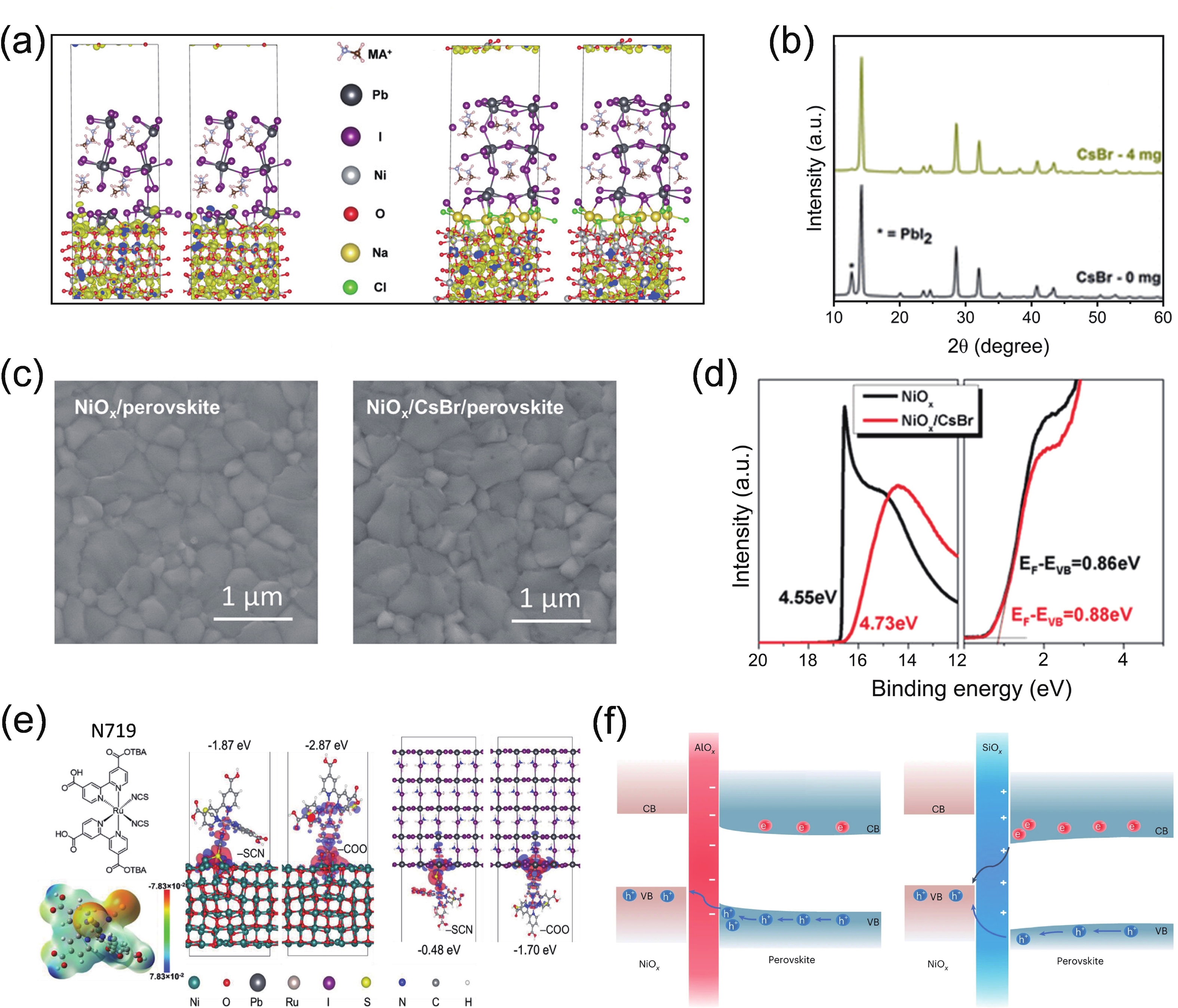
Perovskite solar cells (PSCs) have become a hot topic in the field of renewable energy due to their excellent power conversion efficiency and potential for low-cost manufacturing. The hole transport layer (HTL), as a key component of PSCs, plays a crucial role in the cell's overall performance. Magnetron sputtering NiOx has attracted widespread attention due to its high carrier mobility, excellent stability, and suitability for large-scale production. Herein, an insightful summary of the recent progress of magnetron sputtering NiOx as the HTL of PSCs is presented to promote its further development. This review summarized the basic properties of magnetron sputtering NiOx thin film, the key parameters affecting the optoelectronic properties of NiOx thin films during the magnetron-sputtering process, and the performance of the corresponding PSCs. Special attention was paid to the interfacial issues between NiOx and perovskites, and the modification strategies were systematically summarized. Finally, the challenges of sputtering NiOx technology and the possible development opportunities were concluded and discussed.-
Keywords:
- magnetron sputtering,
- NiOx,
- perovskite,
- solar cells
-
References
[1] Liu B F, Bai L S, Li T T, et al. High efficiency and high open-circuit voltage quadruple-junction silicon thin film solar cells for future electronic applications. Energy Environ Sci, 2017, 10, 1134 doi: 10.1039/C7EE00332C[2] Yang X B, Kang J X, Liu W Z, et al. Solution-doped polysilicon passivating contacts for silicon solar cells. ACS Appl Mater Interfaces, 2021, 13, 8455 doi: 10.1021/acsami.0c22127[3] Ramanujam J, Singh U P. Copper indium gallium selenide based solar cells–a review. Energy Environ Sci, 2017, 10, 1306 doi: 10.1039/C7EE00826K[4] Poplawsky J D. Cadmium telluride solar cells: Record-breaking voltages. Nat Energy, 2016, 1, 16021 doi: 10.1038/nenergy.2016.21[5] NREL. Best research-cell efficiency chart from the national renewable energy laboratory.[6] Jo J W, Seo M S, Park M, et al. Improving performance and stability of flexible planar-heterojunction perovskite solar cells using polymeric hole-transport material. Adv Funct Mater, 2016, 26, 4464 doi: 10.1002/adfm.201600746[7] Zhao D W, Sexton M, Park H Y, et al. High-efficiency solution-processed planar perovskite solar cells with a polymer hole transport layer. Adv Energy Mater, 2015, 5, 1401855 doi: 10.1002/aenm.201401855[8] Kim Y, Jung E H, Kim G, et al. Sequentially fluorinated PTAA polymers for enhancing VOC of high-performance perovskite solar cells. Adv Energy Mater, 2018, 8, 1801668 doi: 10.1002/aenm.201801668[9] Fei C B, Kuvayskaya A, Shi X Q, et al. Strong-bonding hole-transport layers reduce ultraviolet degradation of perovskite solar cells. Science, 2024, 384, 1126 doi: 10.1126/science.adi4531[10] Reza K M, Gurung A, Bahrami B, et al. Tailored PEDOT: PSS hole transport layer for higher performance in perovskite solar cells: Enhancement of electrical and optical properties with improved morphology. J Energy Chem, 2020, 44, 41 doi: 10.1016/j.jechem.2019.09.014[11] Wei Q S, Mukaida M, Naitoh Y, et al. Morphological change and mobility enhancement in PEDOT: PSS by adding co-solvents. Adv Mater, 2013, 25, 2831 doi: 10.1002/adma.201205158[12] Chen S C, Kuo T, Lin H C, et al. Optoelectronic properties of p-type NiO films deposited by direct current magnetron sputtering versus high power impulse magnetron sputtering. Appl Surf Sci, 2020, 508, 145106 doi: 10.1016/j.apsusc.2019.145106[13] Chen Z H, Qin S H, Jin J Y, et al. Manipulating carrier concentration by self-assembled monolayers in thermoelectric polymer thin films. ACS Appl Mater Interfaces, 2021, 13, 32067 doi: 10.1021/acsami.1c04020[14] Feng M L, Wang M, Zhou H P, et al. Optoelectronic modulation of undoped NiOx films for inverted perovskite solar cells via intrinsic defect regulation. ACS Appl Energy Mater, 2020, 3, 9732 doi: 10.1021/acsaem.0c01330[15] Kim H, Kumar M D, Patel M, et al. ITO nanowires-embedding transparent NiO/ZnO photodetector. Mater Res Bull, 2016, 83, 35 doi: 10.1016/j.materresbull.2016.05.025[16] Li X Q, Li D P, Xu J C, et al. Mesoporous-structure enhanced gas-sensing properties of nickel oxides nanowires. Mater Res Bull, 2017, 89, 280 doi: 10.1016/j.materresbull.2017.02.009[17] Mohammad S M, Hassan Z, Abd-Alghafour N M, et al. Ultraviolet electroluminescence from flowers-like n-ZnO nanorods/p-GaN light-emitting diode fabricated by modified chemical bath deposition. J Lumin, 2020, 226, 117510 doi: 10.1016/j.jlumin.2020.117510[18] Li Z, Sun X L, Zheng X P, et al. Stabilized hole-selective layer for high-performance inverted p-i-n perovskite solar cells. Science, 2023, 382, 284 doi: 10.1126/science.ade9637[19] Qiu Z W, Gong H B, Zheng G, et al. Enhanced physical properties of pulsed laser deposited NiO films via annealing and lithium doping for improving perovskite solar cell efficiency. J Mater Chem C, 2017, 5, 7084 doi: 10.1039/C7TC01224A[20] Li G J, Jiang Y B, Deng S B, et al. Overcoming the limitations of sputtered nickel oxide for high-efficiency and large-area perovskite solar cells. Adv Sci, 2017, 4, 1700463 doi: 10.1002/advs.201700463[21] Abzieher T, Moghadamzadeh S, Schackmar F, et al. Electron-beam-evaporated nickel oxide hole transport layers for perovskite-based photovoltaics. Adv Energy Mater, 2019, 9, 1802995 doi: 10.1002/aenm.201802995[22] Phung N, Verheijen M, Todinova A, et al. Enhanced self-assembled monolayer surface coverage by ALD NiO in p-i-n perovskite solar cells. ACS Appl Mater Interfaces, 2022, 14, 2166 doi: 10.1021/acsami.1c15860[23] Liu S W, Li J B, Xiao W S, et al. Buried interface molecular hybrid for inverted perovskite solar cells. Nature, 2024, 632, 536 doi: 10.1038/s41586-024-07723-3[24] Son M K, Steier L, Schreier M, et al. A copper nickel mixed oxide hole selective layer for Au-free transparent cuprous oxide photocathodes. Energy Environ Sci, 2017, 10, 912 doi: 10.1039/C6EE03613A[25] Pan L, Liu C, Zhu H, et al. Fine modification of reactively sputtered NiOX hole transport layer for application in all-inorganic CsPbI2Br perovskite solar cells. Sol Energy, 2020, 196, 521 doi: 10.1016/j.solener.2019.12.056[26] Zhang J Y, Li W W, Hoye R L Z, et al. Electronic and transport properties of Li-doped NiO epitaxial thin films. J Mater Chem C, 2018, 6, 2275 doi: 10.1039/C7TC05331B[27] Yin X T, Guo Y X, Xie H X, et al. Nickel oxide as efficient hole transport materials for perovskite solar cells. Sol RRL, 2019, 3, 1900001 doi: 10.1002/solr.201900001[28] Chang C Y, Wu Y W, Yang S H, et al. Preparation of nickel oxide nanoflakes for carrier extraction and transport in perovskite solar cells. Nanomaterials, 2022, 12, 3336 doi: 10.3390/nano12193336[29] Dewan S, Tomar M, Tandon R P, et al. Zn doping induced conductivity transformation in NiO films for realization of p-n homo junction diode. J Appl Phys, 2017, 121, 215307 doi: 10.1063/1.4984580[30] Liu Z H, Zhu A L, Cai F S, et al. Nickel oxide nanoparticles for efficient hole transport in p-i-n and n-i-p perovskite solar cells. J Mater Chem A, 2017, 5, 6597 doi: 10.1039/C7TA01593C[31] Ochoa-Martinez E, Bijani-Chiquero S, Del Valle Martínez de Yuso M, et al. Nanocrystalline flash annealed nickel oxide for large area perovskite solar cells. Adv Sci, 2023, 10, 2302549 doi: 10.1002/advs.202302549[32] Usha K S, Sivakumar R, Sanjeeviraja C. Preparation of pure NiO thin film by radio frequency magnetron sputtering technique and investigation on its properties. J Mater Sci Mater Electron, 2022, 33, 16136 doi: 10.1007/s10854-022-08504-2[33] Xie X, Gao C, Du X, et al. Improved optical and electrochromic properties of NiOx films by low-temperature spin-coating method based on NiOx nanoparticles. Materials, 2018, 11, 760 doi: 10.3390/ma11050760[34] Hossain M I, Mahmud Hasan A K, Qarony W, et al. Electrical and optical properties of nickel-oxide films for efficient perovskite solar cells. Small Meth, 2020, 4, 2000454 doi: 10.1002/smtd.202000454[35] Kwon Y H, Chun S H, Han J H, et al. Correlation between electrical properties and point defects in NiO thin films. Met Mater Int, 2012, 18, 1003 doi: 10.1007/s12540-012-6012-5[36] Salunkhe P, Ali A V M, Kekuda D. Structural, spectroscopic and electrical properties of dc magnetron sputtered NiO thin films and an insight into different defect states. Appl Phys A, 2021, 127, 390 doi: 10.1007/s00339-021-04501-0[37] Kim S K, Seok H J, Kim D H, et al. Comparison of NiOx thin film deposited by spin-coating or thermal evaporation for application as a hole transport layer of perovskite solar cells. RSC Adv, 2020, 10, 43847 doi: 10.1039/D0RA08776A[38] Yu S Q, Xiong Z, Zhou H T, et al. Homogenized NiOx nanoparticles for improved hole transport in inverted perovskite solar cells. Science, 2023, 382, 1399 doi: 10.1126/science.adj8858[39] You J B, Meng L, Song T B, et al. Improved air stability of perovskite solar cells via solution-processed metal oxide transport layers. Nat Nanotechnol, 2016, 11, 75 doi: 10.1038/nnano.2015.230[40] Mahmoudi T, Wang Y S, Hahn Y B. Highly stable perovskite solar cells based on perovskite/NiO-graphene composites and NiO interface with 25.9mA/cm2 photocurrent density and 20.8% efficiency. Nano Energy, 2021, 79, 105452 doi: 10.1016/j.nanoen.2020.105452[41] Park S, Kim D W, Park S Y. Improved stability and efficiency of inverted perovskite solar cell by employing nickel oxide hole transporting material containing ammonium salt stabilizer. Adv Funct Mater, 2022, 32, 2200437 doi: 10.1002/adfm.202200437[42] Ukoba K O, Eloka-Eboka A C, Inambao F L. Review of nanostructured NiO thin film deposition using the spray pyrolysis technique. Renew Sustain Energy Rev, 2018, 82, 2900 doi: 10.1016/j.rser.2017.10.041[43] Scheideler W J, Rolston N, Zhao O, et al. Rapid aqueous spray fabrication of robust NiOx: A simple and scalable platform for efficient perovskite solar cells. Adv Energy Mater, 2019, 9, 1803600 doi: 10.1002/aenm.201803600[44] Cai X, Hu T, Hou H, et al. A review for nickel oxide hole transport layer and its application in halide perovskite solar cells. Mater Today Sustain, 2023, 23, 100438 doi: 10.1016/j.mtsust.2023.100438[45] Subbiah A S, Halder A, Ghosh S, et al. Inorganic hole conducting layers for perovskite-based solar cells. J Phys Chem Lett, 2014, 5, 1748 doi: 10.1021/jz500645n[46] Shepelin N A, Tehrani Z P, Ohannessian N, et al. A practical guide to pulsed laser deposition. Chem Soc Rev, 2023, 52, 2294 doi: 10.1039/D2CS00938B[47] Park J H, Seo J, Park S, et al. Efficient CH3NH3PbI3 perovskite solar cells employing nanostructured p-type NiO electrode formed by a pulsed laser deposition. Adv Mater, 2015, 27, 4013 doi: 10.1002/adma.201500523[48] Yu X T, Liu C, Li C, et al. Controlled NiOx defect engineering to harnessing redox reactions in perovskite photovoltaic cells via atomic layer deposition. ACS Appl Mater Interfaces, 2024, 16, 31114 doi: 10.1021/acsami.4c03761[49] Park H, Nandi P, In Y, et al. Practical and thermal atomic layer deposition of NiO as hole-transporting layers for inverted perovskite solar cells. Sol RRL, 2024, 8, 2300858 doi: 10.1002/solr.202300858[50] Yadav P, Ajitha B, Reddy Y, et al. Effect of sputter pressure on UV photodetector performance of WO3 thin films. Appl Surf Sci, 2021, 536, 147947 doi: 10.1016/j.apsusc.2020.147947[51] Singh P, Kaur D. Room temperature growth of nanocrystalline anatase TiO2 thin films by dc magnetron sputtering. Phys B Condens Matter, 2010, 405, 1258 doi: 10.1016/j.physb.2009.11.061[52] Yan M Y, Xiang T X, Yu X X, et al. Room-temperature sputtered NiOx for hysteresis-free and stable inverted Cs-FA mixed-cation perovskite solar cells. Mater Sci Semicond Process, 2020, 115, 105129 doi: 10.1016/j.mssp.2020.105129[53] Islam M B, Yanagida M, Shirai Y, et al. NiOx hole transport layer for perovskite solar cells with improved stability and reproducibility. ACS Omega, 2017, 2, 2291 doi: 10.1021/acsomega.7b00538[54] Erdenebileg E, Tiwari N, Kosasih F U, et al. Co-evaporated p-i-n perovskite solar cells with sputtered NiOx hole transport layer. Mater Today Chem, 2023, 30, 101575 doi: 10.1016/j.mtchem.2023.101575[55] Ashok Kumar Reddy Y, Sivasankar Reddy A, Sreedhara Reddy P. Substrate temperature dependent properties of Cu doped NiO films deposited by DC reactive magnetron sputtering. J Mater Sci Technol, 2013, 29, 647 doi: 10.1016/j.jmst.2013.03.005[56] Tao Y, Zhu B L, Yang Y T, et al. The structural, electrical, and optical properties of SnO2 films prepared by reactive magnetron sputtering: Influence of substrate temperature and O2 flow rate. Mater Chem Phys, 2020, 250, 123129 doi: 10.1016/j.matchemphys.2020.123129[57] Zheng X L, Song Z N, Chen Z L, et al. Interface modification of sputtered NiOx as the hole-transporting layer for efficient inverted planar perovskite solar cells. J Mater Chem C, 2020, 8, 1972 doi: 10.1039/C9TC05759E[58] Hwang J D, Ho T H. Effects of oxygen content on the structural, optical, and electrical properties of NiO films fabricated by radio-frequency magnetron sputtering. Mater Sci Semicond Process, 2017, 71, 396 doi: 10.1016/j.mssp.2017.09.002[59] Tuna Ö, Mak A K, Öztürk O, et al. Influence of oxygen partial pressure on the structural, optical and electrochromic properties of NiO thin films grown by magnetron sputtering. Appl Phys A, 2023, 129, 820 doi: 10.1007/s00339-023-07090-2[60] Huang A B, Lei L, Chen Y X, et al. Minimizing the energy loss of perovskite solar cells with Cu+ doped NiOx processed at room temperature. Sol Energy Mater Sol Cells, 2018, 182, 128 doi: 10.1016/j.solmat.2018.01.025[61] Huang A B, Zhu J T, Zheng J Y, et al. Achieving high-performance planar perovskite solar cells with co-sputtered Co-doping NiOx hole transport layers by efficient extraction and enhanced mobility. J Mater Chem C, 2016, 4, 10839 doi: 10.1039/C6TC03624D[62] Nie W Y, Tsai H, Blancon J C, et al. Critical role of interface and crystallinity on the performance and photostability of perovskite solar cell on nickel oxide. Adv Mater, 2018, 30, 1703879 doi: 10.1002/adma.201703879[63] Wei Y, Yao K, Wang X F, et al. Improving the efficiency and environmental stability of inverted planar perovskite solar cells via silver-doped nickel oxide hole-transporting layer. Appl Surf Sci, 2018, 427, 782 doi: 10.1016/j.apsusc.2017.08.184[64] Zhang W, Shen H L, Ge J W, et al. Magnetron sputtered Al-doped NiOx films as a hole transport layer for perovskite solar cells. J Mater Sci, 2022, 57, 15889 doi: 10.1007/s10853-022-07614-w[65] Alghamdi A R M, Yanagida M, Shirai Y, et al. Surface passivation of sputtered NiOx using a SAM interface layer to enhance the performance of perovskite solar cells. ACS Omega, 2022, 7, 12147 doi: 10.1021/acsomega.2c00509[66] Yan X, Zheng J H, Zheng L L, et al. Optimization of sputtering NiOx films for perovskite solar cell applications. Mater Res Bull, 2018, 103, 150 doi: 10.1016/j.materresbull.2018.03.027[67] Guo T, Yun S, Li Y X, et al. Magnetron sputtered all-metal-oxide layers with balanced charge carrier transport efficiency for long-term stable perovskite solar cells. Sol Energy, 2020, 208, 652 doi: 10.1016/j.solener.2020.08.034[68] Aydin E, Troughton J, De Bastiani M, et al. Room-temperature-sputtered nanocrystalline nickel oxide as hole transport layer for p–i–n perovskite solar cells. ACS Appl Energy Mater, 2018, 1, 6227 doi: 10.1021/acsaem.8b01263[69] Itzhak A, He X, Kama A D, et al. NiN-passivated NiO hole-transport layer improves halide perovskite-based solar cell. ACS Appl Mater Interfaces, 2022, 14, 47587 doi: 10.1021/acsami.2c11701[70] Sun J J, Shou C H, Sun J S, et al. NiO-seeded self-assembled monolayers as highly hole-selective passivating contacts for efficient inverted perovskite solar cells. Sol RRL, 2021, 5, 2100663 doi: 10.1002/solr.202100663[71] Zhumagali S, Isikgor F H, Maity P, et al. Linked nickel oxide/perovskite interface passivation for high-performance textured monolithic tandem solar cells. Adv Energy Mater, 2021, 11, 2101662 doi: 10.1002/aenm.202101662[72] Tutundzic M, Zhang X, Lammar S, et al. Toward efficient and fully scalable sputtered NiO-based inverted perovskite solar modules via co-ordinated modification strategies. Sol RRL, 2024, 8, 2300862 doi: 10.1002/solr.202300862[73] Wang L, Zhang T, Yuan S H, et al. Over 19% efficiency perovskite solar modules by simultaneously suppressing cation deprotonation and iodide oxidation. ACS Appl Mater Interfaces, 2024, 16, 4751 doi: 10.1021/acsami.3c16317[74] Zhang X, Qiu W M, Apergi S, et al. Minimizing the interface-driven losses in inverted perovskite solar cells and modules. ACS Energy Lett, 2023, 8, 2532 doi: 10.1021/acsenergylett.3c00697[75] Mao L, Yang T, Zhang H, et al. Fully textured, production-line compatible monolithic perovskite/silicon tandem solar cells approaching 29% efficiency. Adv Mater, 2022, 34, 2206193 doi: 10.1002/adma.202206193[76] Gostishchev P, Luchnikov L O, Bronnikov O, et al. Ion-beam sputtering of NiOx hole transporting layers for p–i–n halide perovskite solar cells. ACS Appl Energy Mater, 2024, 7, 919 doi: 10.1021/acsaem.3c01967[77] Niu G D, Wang S Y, Li J W, et al. Oxygen doping in nickel oxide for highly efficient planar perovskite solar cells. J Mater Chem A, 2018, 6, 4721 doi: 10.1039/C8TA00161H[78] Xia X F, Jiang Y H, Wan Q X, et al. Lithium and silver co-doped nickel oxide hole-transporting layer boosting the efficiency and stability of inverted planar perovskite solar cells. ACS Appl Mater Interfaces, 2018, 10, 44501 doi: 10.1021/acsami.8b16649[79] Mann D S, Kwon S N, Thakur S, et al. Suppressing redox reactions at the perovskite-nickel oxide interface with zinc nitride to improve the performance of perovskite solar cells. Small, 2024, 20, 2311362 doi: 10.1002/smll.202311362[80] Boyd C C, Shallcross R C, Moot T, et al. Overcoming redox reactions at perovskite-nickel oxide interfaces to boost voltages in perovskite solar cells. Joule, 2020, 4, 1759 doi: 10.1016/j.joule.2020.06.004[81] Tang H C, Shen Z C, Shen Y Z, et al. Reinforcing self-assembly of hole transport molecules for stable inverted perovskite solar cells. Science, 2024, 383, 1236 doi: 10.1126/science.adj9602[82] Cao Q, Wang T Y, Pu X Y, et al. Co-self-assembled monolayers modified NiO for stable inverted perovskite solar cells. Adv Mater, 2024, 36, 2311970 doi: 10.1002/adma.202311970[83] Jin Y B, Feng H P, Li Y J, et al. Recrystallizing sputtered NiOx for improved hole extraction in perovskite/silicon tandem solar cells. Adv Energy Mater, 2024, 2403911 doi: 10.1002/aenm.202403911[84] Chen W, Zhou Y C, Chen G C, et al. Alkali chlorides for the suppression of the interfacial recombination in inverted planar perovskite solar cells. Adv Energy Mater, 2019, 9, 1803872 doi: 10.1002/aenm.201803872[85] Pant N, Kulkarni A, Yanagida M, et al. Passivation of bulk and interface defects in sputtered-NiOx-based planar perovskite solar cells: A facile interfacial engineering strategy with alkali metal halide salts. ACS Appl Energy Mater, 2021, 4, 4530 doi: 10.1021/acsaem.1c00032[86] Zhang B J, Su J, Guo X, et al. NiO/perovskite heterojunction contact engineering for highly efficient and stable perovskite solar cells. Adv Sci, 2020, 7, 1903044 doi: 10.1002/advs.201903044[87] Xiao K, Lin Y H, Zhang M, et al. Scalable processing for realizing 21.7%-efficient all-perovskite tandem solar modules. Science, 2022, 376, 762 doi: 10.1126/science.abn7696[88] Li H Y, Zhang C, Gong C, et al. 2D/3D heterojunction engineering at the buried interface towards high-performance inverted methylammonium-free perovskite solar cells. Nat Energy, 2023, 8, 946 doi: 10.1038/s41560-023-01295-8[89] Yang Y H, Cheng S Y, Zhu X L, et al. Inverted perovskite solar cells with over 2, 000 h operational stability at 85 °C using fixed charge passivation. Nat Energy, 2024, 9, 37 doi: 10.1038/s41560-023-01377-7 -
Proportional views


