


Fig. 1.
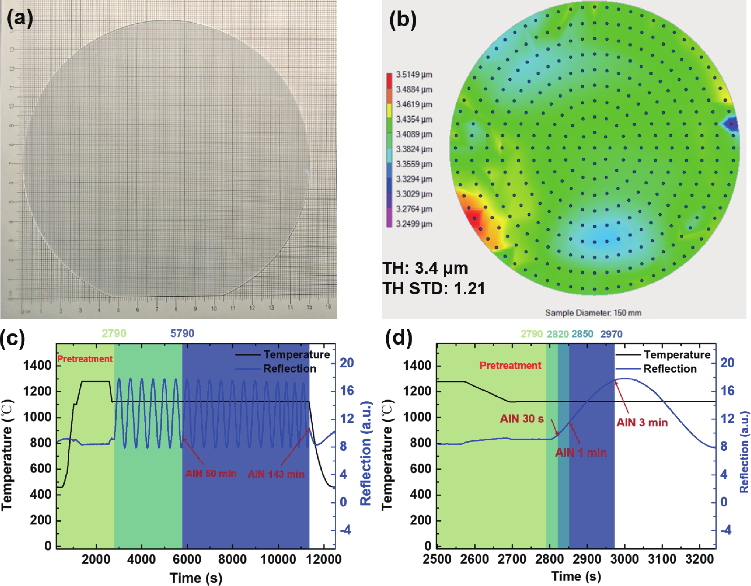
(Color online) (a) Photograph of the 6-inch AlN wafer. (b) Thickness mapping of the AlN wafer. The temperature and reflection curves of (c) the AlN growth process, and (d) a magnified view of the graph in (c).
ARTICLES
Shunpeng Lu1, 2, Jianwei Ben1, 2, Ke Jiang1, 2, Shanli Zhang1, 2, Ruojia Zhang1, 2, Jialong Hao1, 2, Zhongxu Liu1, 2, Wenchao Sun1, 2, Zikai Nie1, 2, Xiaojuan Sun1, 2, and Dabing Li1, 2,
Corresponding author: Xiaojuan Sun, sunxj@ciomp.ac.cn; Dabing Li, lidb@ciomp.ac.cn
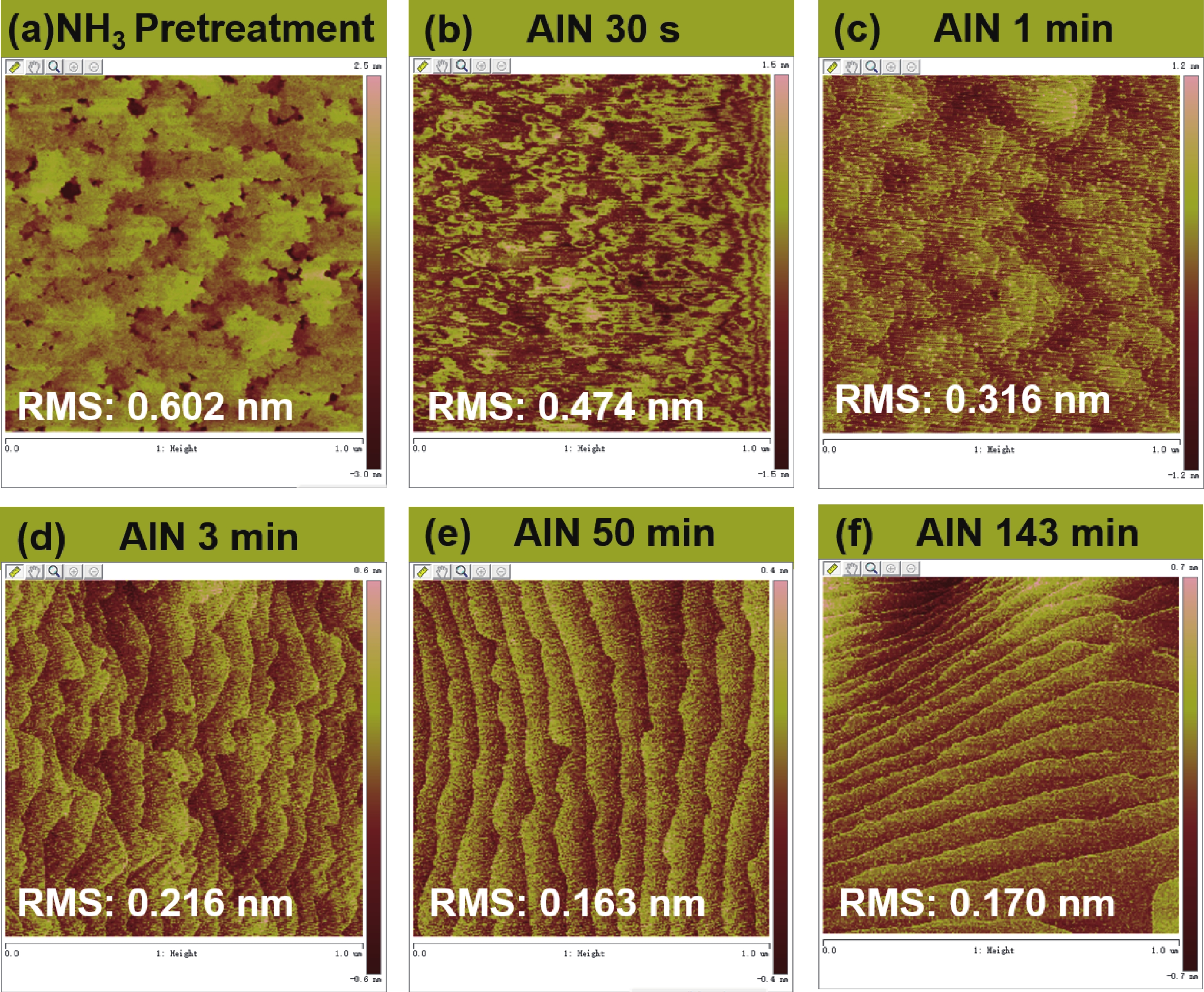
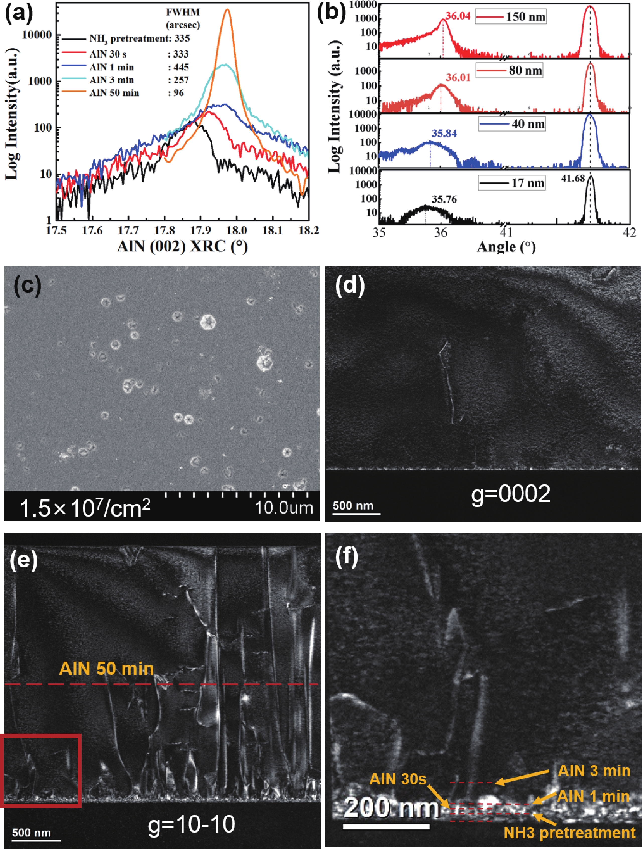
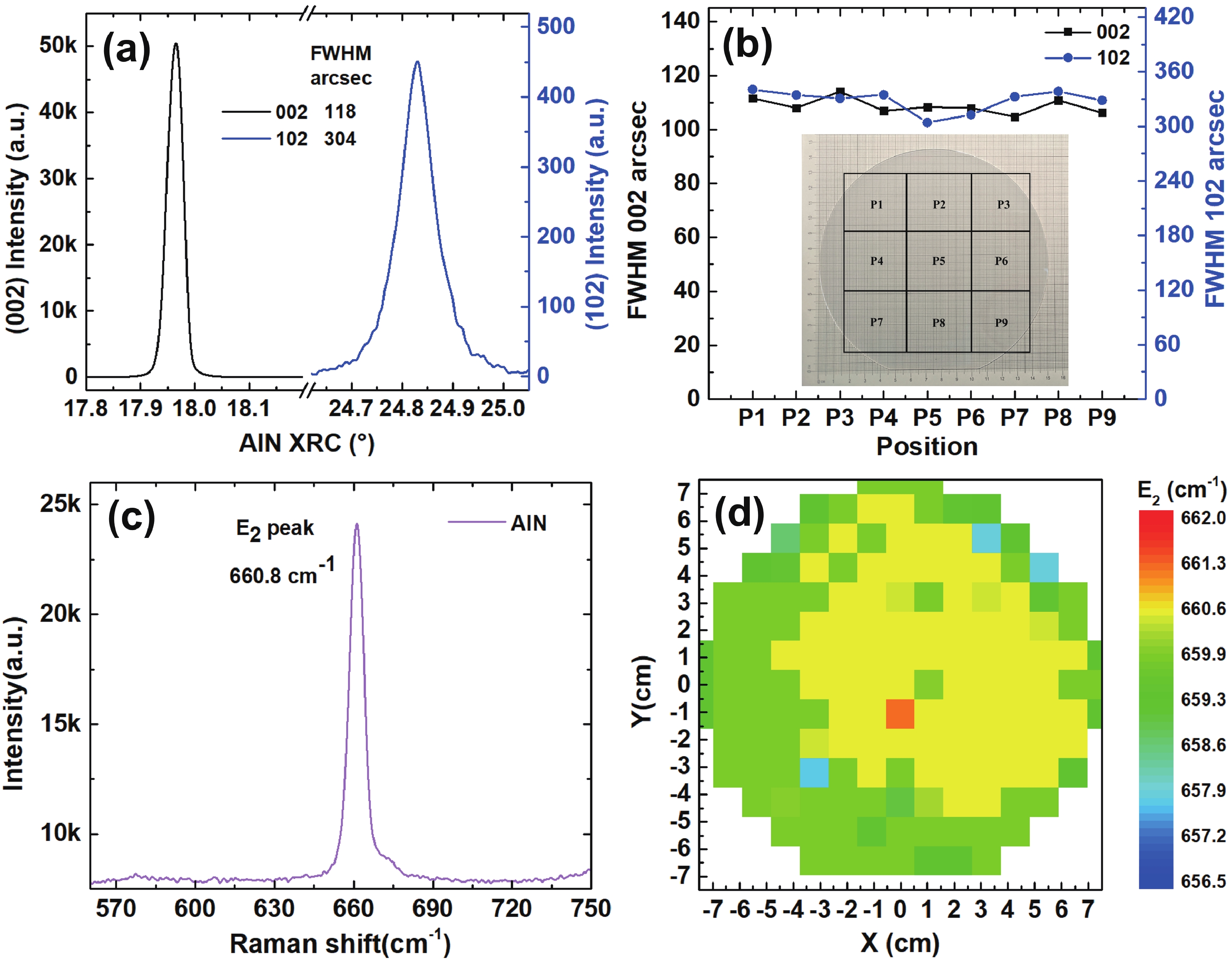
Abstract: High-quality AlN epitaxial layers with low dislocation densities and uniform crystal quality are essential for next-generation optoelectronic and power devices. This study reports the epitaxial growth of 6-inch AlN films on 17 nm AlN/sapphire templates using metal−organic chemical vapor deposition (MOCVD). Comprehensive characterization reveals significant advancements in crystal quality and uniformity. Atomic force microscopy (AFM) shows progressive surface roughness reduction during early growth stages, achieving stabilization at a root mean square (RMS) roughness of 0.216 nm within 3 min, confirming successful 2D growth mode. X-ray rocking curve (XRC) analysis indicates a marked reduction in the (0002) reflection full width at half maximum (FWHM), from 445 to 96 arcsec, evidencing effective dislocation annihilation. Transmission electron microscopy (TEM) demonstrates the elimination of edge dislocations near the AlN template interface. Stress analysis highlights the role of a highly compressive 17 nm AlN template (5.11 GPa) in facilitating threading dislocation bending and annihilation, yielding a final dislocation density of ~1.5 × 107 cm−2. Raman spectroscopy and XRC mapping confirm excellent uniformity of stress and crystal quality across the wafer. These findings demonstrate the feasibility of this method for producing high-quality, large-area, atomically flat AlN films, advancing applications in optoelectronics and power electronics.
Keywords: AlN, 6-inch, MOCVD, threading dislocation density, optoelectronic, power electronics
| [1] |
Nela L, Ma J, Erine C, et al. Multi-channel nanowire devices for efficient power conversion. Nat Electron, 2021, 4, 284 doi: 10.1038/s41928-021-00550-8
|
| [2] |
Kuball M. Multi-channel power transistors shape up. Nat Electron, 2019, 2, 553 doi: 10.1038/s41928-019-0341-z
|
| [3] |
Zhao Y P, Wang C, Zheng X F, et al. Effects of recess depths on performance of AlGaN/GaN power MIS-HEMTs on the Si substrates and threshold voltage model of different recess depths for the using HfO2 gate insulator. Solid State Electron, 2020, 163, 107649 doi: 10.1016/j.sse.2019.107649
|
| [4] |
Lu H, Yang L, Hou B, et al. AlN/GaN/InGaN coupling-channel HEMTs with steep subthreshold swing of sub-60 mV/decade. Appl Phys Lett, 2022, 120, 173502 doi: 10.1063/5.0088585
|
| [5] |
Zhong L J, Xing Y H, Han J, et al. Influence of growth time of AlN interfacial layer on electrical properties of AlGaN/AlN/GaN HEMT materials. Chin J Lumin, 2014, 35, 830 (in Chinese) doi: 10.3788/fgxb20143507.0830
|
| [6] |
Chen X, Xing Y H, Han J, et al. Influence of Al composition on electrical and structural properties of AlxGa1-xN/AlN/GaN HEMT materials grown by MOCVD. Chin J Lumin, 2013, 34, 1646 (in Chinese) doi: 10.3788/fgxb20133412.1646
|
| [7] |
Feng F, Liu Y B, Zhang K, et al. High-power AlGaN deep-ultraviolet micro-light-emitting diode displays for maskless photolithography. Nat Photonics, 2025, 19, 101 doi: 10.1038/s41566-024-01551-7
|
| [8] |
Jiang K, Sun X J, Shi Z M, et al. Quantum engineering of non-equilibrium efficient p-doping in ultra-wide band-gap nitrides. Light Sci Appl, 2021, 10, 69 doi: 10.1038/s41377-021-00503-y
|
| [9] |
Cai Q, You H F, Guo H, et al. Progress on AlGaN-based solar-blind ultraviolet photodetectors and focal plane arrays. Light Sci Appl, 2021, 10, 94 doi: 10.1038/s41377-021-00527-4
|
| [10] |
Li D B, Jiang K, Sun X J, et al. AlGaN photonics: Recent advances in materials and ultraviolet devices. Adv Opt Photonics, 2018, 10, 43 doi: 10.1364/AOP.10.000043
|
| [11] |
Li H B, Lu S P, Zhu L C, et al. Efficiency boosting of 236 nm AlGaN-based micro-LEDs. J Phys D: Appl Phys, 2025, 58, 015109 doi: 10.1088/1361-6463/ad714b
|
| [12] |
Li L, Xu Y, Cao B, et al. Epitaxial growth and optoelectronic properties of AlGaN-Based deep-ultraviolet LED. J Synth Cryst, 2022, 51, 5
|
| [13] |
Bahamonde J A, Kymissis I. A reconfigurable surface acoustic wave filter on ZnO/AlGaN/GaN heterostructure. IEEE Trans Electron Devices, 2020, 67, 4507 doi: 10.1109/TED.2020.3018697
|
| [14] |
Hohkawa K, Koh K, Nishimura K, et al. DC variable harmonic pass band operation of AlGaN/GaN surface acoustic wave devices. Jpn J Appl Phys, 2008, 47, 7104 doi: 10.1143/JJAP.47.7104
|
| [15] |
Jiang W B, Chen J F, Liu X Y, et al. Thin film aluminum nitride surface acoustic wave resonators for quantum acoustodynamics. Appl Phys Lett, 2023, 123, 024002 doi: 10.1063/5.0158083
|
| [16] |
Lu S P, Bai J X, Li H B, et al. 240 nm AlGaN-based deep ultraviolet micro-LEDs: Size effect versus edge effect. J Semicond, 2024, 45, 012504 doi: 10.1088/1674-4926/45/1/012504
|
| [17] |
Gu G D, Dun S B, Lü Y J, et al. Low ohmic contact AlN/GaN HEMTs grown by MOCVD. J Semicond, 2013, 34, 114004 doi: 10.1088/1674-4926/34/11/114004
|
| [18] |
Yang J, Zhao D G, Liu Z S, et al. GaN based ultraviolet laser diodes. J Semicond, 2024, 45, 011501 doi: 10.1088/1674-4926/45/1/011501
|
| [19] |
Deng X G, Han J, Xing Y H, et al. Influence of H2 carrier gas on epitaxy of AlN buffer layer. Chin J Lumin, 2013, 34, 776 (in Chinese) doi: 10.3788/fgxb20133406.0776
|
| [20] |
Jia H, Chen Y R, Sun X J, et al. Effect of AlN interlayer on a plane AlGaN grown by MOCVD. Chin J Lumin, 2012, 33, 519 (in Chinese) doi: 10.3788/fgxb20123305.0519
|
| [21] |
Zheng G Y, Sun Y K, Zhang H, et al. Numerical simulation study on growth rate and gas reaction path of InN-MOCVD with close-coupled showerhead reactor. J Synth Cryst, 2021, 50, 8 (in Chinese) doi: 10.1016/j.jcrysgro.2024.127725
|
| [22] |
Mao Y L, Zuo R. Influence of Inlet structure of planetary reactor on Gas reaction path and growth rate in AlN-MOCVD. J Synth Cryst, 2020, 49, 8 (in Chinese) doi: 10.1016/j.jcrysgro.2020.125942
|
| [23] |
Chen Z, Newman S, Brown D, et al. High quality AlN grown on SiC by metal organic chemical vapor deposition. Appl Phys Lett, 2008, 93, 191906 doi: 10.1063/1.2988323
|
| [24] |
Chen X, Yan J C, Zhang Y, et al. Improved crystalline quality of AlN by epitaxial lateral overgrowth using two-phase growth method for deep-ultraviolet stimulated emission. IEEE Photonics J, 2016, 8, 2300211 doi: 10.1109/JPHOT.2016.2614102
|
| [25] |
Jain R, Sun W, Yang J, et al. Migration enhanced lateral epitaxial overgrowth of AlN and AlGaN for high reliability deep ultraviolet light emitting diodes. Appl Phys Lett, 2008, 93, 051113 doi: 10.1063/1.2969402
|
| [26] |
Zhang L S, Xu F J, Wang J M, et al. High-quality AlN epitaxy on nano-patterned sapphire substrates prepared by nano-imprint lithography. Sci Rep, 2016, 6, 35934 doi: 10.1038/srep35934
|
| [27] |
Xie N, Xu F J, Wang J M, et al. Stress evolution in AlN growth on nano-patterned sapphire substrates. Appl Phys Express, 2020, 13, 015504 doi: 10.7567/1882-0786/ab582c
|
| [28] |
Hagedorn S, Mogilatenko A, Walde S, et al. High-temperature annealing and patterned AlN/sapphire interfaces. Phys Status Solidi B, 2021, 258, 2100187 doi: 10.1002/pssb.202100187
|
| [29] |
Kao Z X, Ye D Q, Yu X, et al. Research and application progress of sapphire substrates. J Synth Cryst, 2018, 47, 6 (in Chinese)
|
| [30] |
Gao Y Q, Yang J K, Wang L L, et al. High-temperature annealing assisted high-quality semipolar (112̅2) AlN film for vacuum ultraviolet detectors. Cryst Growth Des, 2023, 23, 9058 doi: 10.1021/acs.cgd.3c01099
|
| [31] |
Uesugi K, Miyake H. Fabrication of AlN templates by high-temperature face-to-face annealing for deep UV LEDs. Jpn J Appl Phys, 2021, 60, 120502 doi: 10.35848/1347-4065/ac3026
|
| [32] |
Liu S F, Yuan Y, Sheng S S, et al. Four-inch high quality crack-free AlN layer grown on a high-temperature annealed AlN template by MOCVD. J Semicond, 2021, 42, 122804 doi: 10.1088/1674-4926/42/12/122804
|
| [33] |
Su Y, Ben J W, Shi Z M, et al. Regulation of oxygen defects in AlGaN-based epilayers grown on high temperature annealed AlN template. Mater Lett, 2024, 369, 136671 doi: 10.1016/j.matlet.2024.136671
|
| [34] |
Sui J E, Ben J W, Zang H, et al. Mechanism of a-AlN surface morphology evolution by high temperature annealing. Chin J Lumin, 2021, 42, 810 (in Chinese) doi: 10.37188/CJL.20210111
|
| [35] |
Nie Z K, Ben J W, Zhang E T, et al. Evolution of AlN step bunching morphology during high-temperature annealing. J Synth Cryst, 2023, 52, 1016 (in Chinese)
|
| [36] |
Jiang K, Sun X J, Ben J W, et al. The defect evolution in homoepitaxial AlN layers grown by high-temperature metal–organic chemical vapor deposition. CrystEngComm, 2018, 20, 2720 doi: 10.1039/C8CE00287H
|
| [37] |
Wright A F. Elastic property of zinc-blende and wurtzite AlN, GaN, and InN. J Appl Phys, 1997, 82, 2833 doi: 10.1063/1.366114
|


Article views: 2756 Times PDF downloads: 255 Times Cited by: 0 Times
Received: 25 November 2024 Revised: 17 December 2024 Online: Accepted Manuscript: 13 January 2025Uncorrected proof: 17 January 2025Published: 15 February 2025
| Citation: |
Shunpeng Lu, Jianwei Ben, Ke Jiang, Shanli Zhang, Ruojia Zhang, Jialong Hao, Zhongxu Liu, Wenchao Sun, Zikai Nie, Xiaojuan Sun, Dabing Li. 6-inch AlN epitaxial films with low dislocation densities via MOCVD[J]. Journal of Semiconductors, 2025, 46(2): 022501. doi: 10.1088/1674-4926/24110030
****
S P Lu, J W Ben, K Jiang, S L Zhang, R J Zhang, J L Hao, Z X Liu, W C Sun, Z K Nie, X J Sun, and D B Li, 6-inch AlN epitaxial films with low dislocation densities via MOCVD[J]. J. Semicond., 2025, 46(2), 022501 doi: 10.1088/1674-4926/24110030

|
 Shunpeng Lu is currently a professor in Changchun Institute of Optics, Fine Mechanics and Physics, Chinese Academy of Sciences. He received his Ph.D. degree in EEE from Nanyang Technological University, Singapore, in August 2017. His research interests focus on Ⅲ-Nitride material MOCVD growth and micro-LED device processing
 Xiaojuan Sun is a professor worked in Changchun Institute of Optics, Fine Mechanics and Physics, Chinese Academy of Sciences (CIOMP, CAS). She received her Ph.D. degree in Condensed Matter Physics from CIOMP, CAS. Her research interests focus on the physics, the Ⅲ-nitride materials and photoelectric devices
 Dabing Li is a professor of Changchun Institute of Optics, Fine Mechanics and Physics, Chinese Academy of Sciences (CIOMP, CAS). He received the Ph.D. degree from the Institute of Semiconductors, CAS in 2004 and then he worked as a postdoctoral and visiting scholar in Mie University until 2008. His research interests include the physics, the Ⅲ-nitride materials and photoelectric devices
| [1] |
Nela L, Ma J, Erine C, et al. Multi-channel nanowire devices for efficient power conversion. Nat Electron, 2021, 4, 284 doi: 10.1038/s41928-021-00550-8
|
| [2] |
Kuball M. Multi-channel power transistors shape up. Nat Electron, 2019, 2, 553 doi: 10.1038/s41928-019-0341-z
|
| [3] |
Zhao Y P, Wang C, Zheng X F, et al. Effects of recess depths on performance of AlGaN/GaN power MIS-HEMTs on the Si substrates and threshold voltage model of different recess depths for the using HfO2 gate insulator. Solid State Electron, 2020, 163, 107649 doi: 10.1016/j.sse.2019.107649
|
| [4] |
Lu H, Yang L, Hou B, et al. AlN/GaN/InGaN coupling-channel HEMTs with steep subthreshold swing of sub-60 mV/decade. Appl Phys Lett, 2022, 120, 173502 doi: 10.1063/5.0088585
|
| [5] |
Zhong L J, Xing Y H, Han J, et al. Influence of growth time of AlN interfacial layer on electrical properties of AlGaN/AlN/GaN HEMT materials. Chin J Lumin, 2014, 35, 830 (in Chinese) doi: 10.3788/fgxb20143507.0830
|
| [6] |
Chen X, Xing Y H, Han J, et al. Influence of Al composition on electrical and structural properties of AlxGa1-xN/AlN/GaN HEMT materials grown by MOCVD. Chin J Lumin, 2013, 34, 1646 (in Chinese) doi: 10.3788/fgxb20133412.1646
|
| [7] |
Feng F, Liu Y B, Zhang K, et al. High-power AlGaN deep-ultraviolet micro-light-emitting diode displays for maskless photolithography. Nat Photonics, 2025, 19, 101 doi: 10.1038/s41566-024-01551-7
|
| [8] |
Jiang K, Sun X J, Shi Z M, et al. Quantum engineering of non-equilibrium efficient p-doping in ultra-wide band-gap nitrides. Light Sci Appl, 2021, 10, 69 doi: 10.1038/s41377-021-00503-y
|
| [9] |
Cai Q, You H F, Guo H, et al. Progress on AlGaN-based solar-blind ultraviolet photodetectors and focal plane arrays. Light Sci Appl, 2021, 10, 94 doi: 10.1038/s41377-021-00527-4
|
| [10] |
Li D B, Jiang K, Sun X J, et al. AlGaN photonics: Recent advances in materials and ultraviolet devices. Adv Opt Photonics, 2018, 10, 43 doi: 10.1364/AOP.10.000043
|
| [11] |
Li H B, Lu S P, Zhu L C, et al. Efficiency boosting of 236 nm AlGaN-based micro-LEDs. J Phys D: Appl Phys, 2025, 58, 015109 doi: 10.1088/1361-6463/ad714b
|
| [12] |
Li L, Xu Y, Cao B, et al. Epitaxial growth and optoelectronic properties of AlGaN-Based deep-ultraviolet LED. J Synth Cryst, 2022, 51, 5
|
| [13] |
Bahamonde J A, Kymissis I. A reconfigurable surface acoustic wave filter on ZnO/AlGaN/GaN heterostructure. IEEE Trans Electron Devices, 2020, 67, 4507 doi: 10.1109/TED.2020.3018697
|
| [14] |
Hohkawa K, Koh K, Nishimura K, et al. DC variable harmonic pass band operation of AlGaN/GaN surface acoustic wave devices. Jpn J Appl Phys, 2008, 47, 7104 doi: 10.1143/JJAP.47.7104
|
| [15] |
Jiang W B, Chen J F, Liu X Y, et al. Thin film aluminum nitride surface acoustic wave resonators for quantum acoustodynamics. Appl Phys Lett, 2023, 123, 024002 doi: 10.1063/5.0158083
|
| [16] |
Lu S P, Bai J X, Li H B, et al. 240 nm AlGaN-based deep ultraviolet micro-LEDs: Size effect versus edge effect. J Semicond, 2024, 45, 012504 doi: 10.1088/1674-4926/45/1/012504
|
| [17] |
Gu G D, Dun S B, Lü Y J, et al. Low ohmic contact AlN/GaN HEMTs grown by MOCVD. J Semicond, 2013, 34, 114004 doi: 10.1088/1674-4926/34/11/114004
|
| [18] |
Yang J, Zhao D G, Liu Z S, et al. GaN based ultraviolet laser diodes. J Semicond, 2024, 45, 011501 doi: 10.1088/1674-4926/45/1/011501
|
| [19] |
Deng X G, Han J, Xing Y H, et al. Influence of H2 carrier gas on epitaxy of AlN buffer layer. Chin J Lumin, 2013, 34, 776 (in Chinese) doi: 10.3788/fgxb20133406.0776
|
| [20] |
Jia H, Chen Y R, Sun X J, et al. Effect of AlN interlayer on a plane AlGaN grown by MOCVD. Chin J Lumin, 2012, 33, 519 (in Chinese) doi: 10.3788/fgxb20123305.0519
|
| [21] |
Zheng G Y, Sun Y K, Zhang H, et al. Numerical simulation study on growth rate and gas reaction path of InN-MOCVD with close-coupled showerhead reactor. J Synth Cryst, 2021, 50, 8 (in Chinese) doi: 10.1016/j.jcrysgro.2024.127725
|
| [22] |
Mao Y L, Zuo R. Influence of Inlet structure of planetary reactor on Gas reaction path and growth rate in AlN-MOCVD. J Synth Cryst, 2020, 49, 8 (in Chinese) doi: 10.1016/j.jcrysgro.2020.125942
|
| [23] |
Chen Z, Newman S, Brown D, et al. High quality AlN grown on SiC by metal organic chemical vapor deposition. Appl Phys Lett, 2008, 93, 191906 doi: 10.1063/1.2988323
|
| [24] |
Chen X, Yan J C, Zhang Y, et al. Improved crystalline quality of AlN by epitaxial lateral overgrowth using two-phase growth method for deep-ultraviolet stimulated emission. IEEE Photonics J, 2016, 8, 2300211 doi: 10.1109/JPHOT.2016.2614102
|
| [25] |
Jain R, Sun W, Yang J, et al. Migration enhanced lateral epitaxial overgrowth of AlN and AlGaN for high reliability deep ultraviolet light emitting diodes. Appl Phys Lett, 2008, 93, 051113 doi: 10.1063/1.2969402
|
| [26] |
Zhang L S, Xu F J, Wang J M, et al. High-quality AlN epitaxy on nano-patterned sapphire substrates prepared by nano-imprint lithography. Sci Rep, 2016, 6, 35934 doi: 10.1038/srep35934
|
| [27] |
Xie N, Xu F J, Wang J M, et al. Stress evolution in AlN growth on nano-patterned sapphire substrates. Appl Phys Express, 2020, 13, 015504 doi: 10.7567/1882-0786/ab582c
|
| [28] |
Hagedorn S, Mogilatenko A, Walde S, et al. High-temperature annealing and patterned AlN/sapphire interfaces. Phys Status Solidi B, 2021, 258, 2100187 doi: 10.1002/pssb.202100187
|
| [29] |
Kao Z X, Ye D Q, Yu X, et al. Research and application progress of sapphire substrates. J Synth Cryst, 2018, 47, 6 (in Chinese)
|
| [30] |
Gao Y Q, Yang J K, Wang L L, et al. High-temperature annealing assisted high-quality semipolar (112̅2) AlN film for vacuum ultraviolet detectors. Cryst Growth Des, 2023, 23, 9058 doi: 10.1021/acs.cgd.3c01099
|
| [31] |
Uesugi K, Miyake H. Fabrication of AlN templates by high-temperature face-to-face annealing for deep UV LEDs. Jpn J Appl Phys, 2021, 60, 120502 doi: 10.35848/1347-4065/ac3026
|
| [32] |
Liu S F, Yuan Y, Sheng S S, et al. Four-inch high quality crack-free AlN layer grown on a high-temperature annealed AlN template by MOCVD. J Semicond, 2021, 42, 122804 doi: 10.1088/1674-4926/42/12/122804
|
| [33] |
Su Y, Ben J W, Shi Z M, et al. Regulation of oxygen defects in AlGaN-based epilayers grown on high temperature annealed AlN template. Mater Lett, 2024, 369, 136671 doi: 10.1016/j.matlet.2024.136671
|
| [34] |
Sui J E, Ben J W, Zang H, et al. Mechanism of a-AlN surface morphology evolution by high temperature annealing. Chin J Lumin, 2021, 42, 810 (in Chinese) doi: 10.37188/CJL.20210111
|
| [35] |
Nie Z K, Ben J W, Zhang E T, et al. Evolution of AlN step bunching morphology during high-temperature annealing. J Synth Cryst, 2023, 52, 1016 (in Chinese)
|
| [36] |
Jiang K, Sun X J, Ben J W, et al. The defect evolution in homoepitaxial AlN layers grown by high-temperature metal–organic chemical vapor deposition. CrystEngComm, 2018, 20, 2720 doi: 10.1039/C8CE00287H
|
| [37] |
Wright A F. Elastic property of zinc-blende and wurtzite AlN, GaN, and InN. J Appl Phys, 1997, 82, 2833 doi: 10.1063/1.366114
|

 WeChat ID
Journal of Semiconductors © 2017 All Rights Reserved 京ICP备05085259号-2

 DownLoad:

