


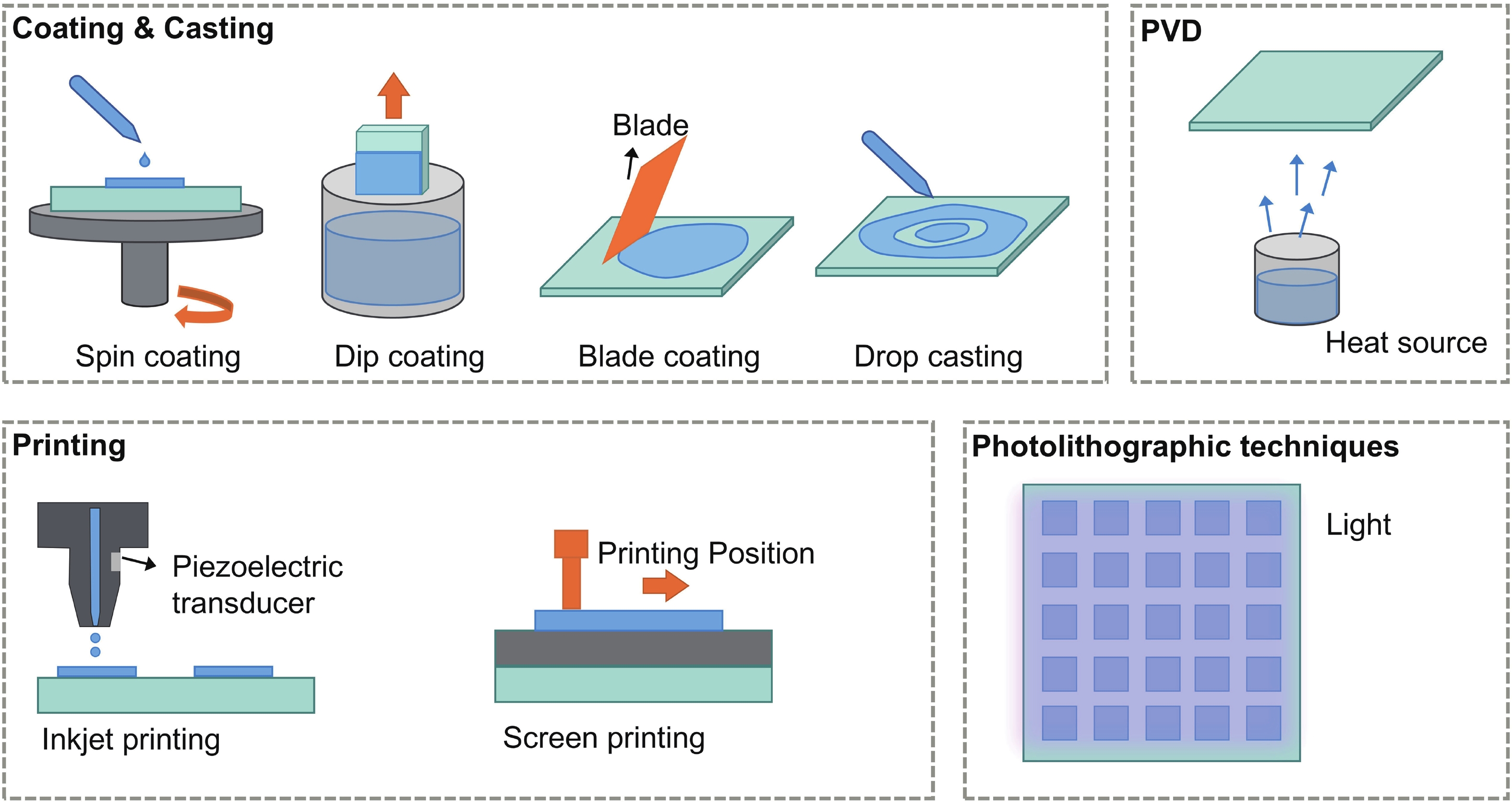
Fig. 1.
(Color online) Schematic diagrams of fabrication strategies of OOSTAs.
SPECIAL ISSUE REVIEWS
Pu Guo, Junyao Zhang and Jia Huang
Corresponding author: Jia Huang, huangjia@tongji.edu.cn
Abstract: The rapid growth of artificial intelligence has accelerated data generation, which increasingly exposes the limitations faced by traditional computational architectures, particularly in terms of energy consumption and data latency. In contrast, data-centric computing that integrates processing and storage has the potential of reducing latency and energy usage. Organic optoelectronic synaptic transistors have emerged as one type of promising devices to implement the data-centric computing paradigm owing to their superiority of flexibility, low cost, and large-area fabrication. However, sophisticated functions including vector-matrix multiplication that a single device can achieve are limited. Thus, the fabrication and utilization of organic optoelectronic synaptic transistor arrays (OOSTAs) are imperative. Here, we summarize the recent advances in OOSTAs. Various strategies for manufacturing OOSTAs are introduced, including coating and casting, physical vapor deposition, printing, and photolithography. Furthermore, innovative applications of the OOSTA system integration are discussed, including neuromorphic visual systems and neuromorphic computing systems. At last, challenges and future perspectives of utilizing OOSTAs in real-world applications are discussed.
Keywords: organic transistor arrays, optoelectronic synaptic transistors, neuromorphic systems, system integration
| [1] |
Sun Z, Kvatinsky S, Si X, et al. A full spectrum of computing-in-memory technologies. Nat Electron, 2023, 6, 823 doi: 10.1038/s41928-023-01053-4
|
| [2] |
van de Burgt Y, Melianas A, Keene S T, et al. Organic electronics for neuromorphic computing. Nat Electron, 2018, 1, 386 doi: 10.1038/s41928-018-0103-3
|
| [3] |
Krestinskaya O, Fouda M E, Benmeziane H, et al. Neural architecture search for in-memory computing-based deep learning accelerators. Nat Rev Electr Eng, 2024, 1, 374 doi: 10.1038/s44287-024-00052-7
|
| [4] |
Aguirre F, Sebastian A, Le Gallo M, et al. Hardware implementation of memristor-based artificial neural networks. Nat Commun, 2024, 15(1), 1974 doi: 10.1038/s41467-024-45670-9
|
| [5] |
Zidan M A, Strachan J P, Lu W D. The future of electronics based on memristive systems. Nat Electron, 2018, 1, 22 doi: 10.1038/s41928-017-0006-8
|
| [6] |
Chen J W, Zhou Z, Kim B J, et al. Optoelectronic graded neurons for bioinspired in-sensor motion perception. Nat Nanotechnol, 2023, 18, 882 doi: 10.1038/s41565-023-01379-2
|
| [7] |
Zhang W Q, Gao B, Tang J S, et al. Neuro-inspired computing chips. Nat Electron, 2020, 3, 371 doi: 10.1038/s41928-020-0435-7
|
| [8] |
Zhou F C, Chai Y. Near-sensor and in-sensor computing. Nat Electron, 2020, 3, 664 doi: 10.1038/s41928-020-00501-9
|
| [9] |
Ren Q Q, Zhu C Y, Ma S J, et al. Optoelectronic devices for in-sensor computing. Adv Mater, 2024, e2407476 doi: 10.1002/adma.202407476
|
| [10] |
Wang Z Q, Wan T Q, Ma S J, et al. Multidimensional vision sensors for information processing. Nat Nanotechnol, 2024, 19, 919 doi: 10.1038/s41565-024-01665-7
|
| [11] |
Wang Y, Yin L, Huang W, et al. Optoelectronic synaptic devices for neuromorphic computing. Adv Intell Syst, 2021, 3, 2000099 doi: 10.1002/aisy.202000099
|
| [12] |
Schuman C D, Kulkarni S R, Parsa M, et al. Opportunities for neuromorphic computing algorithms and applications. Nat Comput Sci, 2022, 2, 10 doi: 10.1038/s43588-021-00184-y
|
| [13] |
Cho S W, Kwon S M, Kim Y H, et al. Recent progress in transistor-based optoelectronic synapses: From neuromorphic computing to artificial sensory system. Adv Intell Syst, 2021, 3, 2000162 doi: 10.1002/aisy.202000162
|
| [14] |
Wan Q Z, Sharbati M T, Erickson J R, et al. Emerging artificial synaptic devices for neuromorphic computing. Adv Mater Technol, 2019, 4, 1900037 doi: 10.1002/admt.201900037
|
| [15] |
Wang X, Ran Y X, Li X Q, et al. Bio-inspired artificial synaptic transistors: Evolution from innovative basic units to system integration. Mater Horiz, 2023, 10, 3269 doi: 10.1039/D3MH00216K
|
| [16] |
He Z H, Shen H G, Ye D K, et al. An organic transistor with light intensity-dependent active photoadaptation. Nat Electron, 2021, 4, 522 doi: 10.1038/s41928-021-00615-8
|
| [17] |
Choi Y, Oh S, Qian C, et al. Vertical organic synapse expandable to 3D crossbar array. Nat Commun, 2020, 11, 4595 doi: 10.1038/s41467-020-17850-w
|
| [18] |
Bu X B, Xu H, Shang D S, et al. Ion-gated transistor: An enabler for sensing and computing integration. Adv Intell Syst, 2020, 2, 2000156 doi: 10.1002/aisy.202000156
|
| [19] |
Li H L, Jiang X T, Ye W B, et al. Fully photon modulated heterostructure for neuromorphic computing. Nano Energy, 2019, 65, 104000 doi: 10.1016/j.nanoen.2019.104000
|
| [20] |
Xiao X Y, Hu J, Tang S, et al. Recent advances in halide perovskite memristors: Materials, structures, mechanisms, and applications. Adv Mater Technol, 2020, 5, 1900914 doi: 10.1002/admt.201900914
|
| [21] |
Duan X G, Cao Z L, Gao K K, et al. Memristor-based neuromorphic chips. Adv Mater, 2024, 36, 2310704 doi: 10.1002/adma.202310704
|
| [22] |
Sarwat S G, Kersting B, Moraitis T, et al. Phase-change memtransistive synapses for mixed-plasticity neural computations. Nat Nanotechnol, 2022, 17, 507 doi: 10.1038/s41565-022-01095-3
|
| [23] |
Jeong B H, Park J, Kim D, et al. Visible light-sensitive artificial photonic synapse. Adv Opt Mater, 2024, 12, 2301652 doi: 10.1002/adom.202301652
|
| [24] |
Wang J, Ilyas N, Ren Y, et al. Technology and integration roadmap for optoelectronic memristor. Adv Mater, 2024, 36, e2307393 doi: 10.1002/adma.202307393
|
| [25] |
Bronstein H, Nielsen C B, Schroeder B C, et al. The role of chemical design in the performance of organic semiconductors. Nat Rev Chem, 2020, 4, 66 doi: 10.1038/s41570-019-0152-9
|
| [26] |
Fuller E J, Keene S T, Melianas A, et al. Parallel programming of an ionic floating-gate memory array for scalable neuromorphic computing. Science, 2019, 364, 570 doi: 10.1126/science.aaw5581
|
| [27] |
Zhang X J, Deng W, Jia R F, et al. Precise patterning of organic semiconductor crystals for integrated device applications. Small, 2019, 15, 1900332 doi: 10.1002/smll.201900332
|
| [28] |
Wang W C, Chi L F. Patterned growth of organic semiconductors for ultra-high resolution microelectronics and optoelectronics. Wearable Electron, 2024, 1, 91 doi: 10.1016/j.wees.2024.05.005
|
| [29] |
Emslie A G, Bonner F T, Peck L G. Flow of a viscous liquid on a rotating disk. J Appl Phys, 1958, 29, 858 doi: 10.1063/1.1723300
|
| [30] |
Sahu N, Parija B, Panigrahi S. Fundamental understanding and modeling of spin coating process: A review. Indian J Phys, 2009, 83, 493 doi: 10.1007/s12648-009-0009-z
|
| [31] |
Hao D D, Zhang J Y, Dai S L, et al. Perovskite/organic semiconductor-based photonic synaptic transistor for artificial visual system. ACS Appl Mater Interfaces, 2020, 12, 39487 doi: 10.1021/acsami.0c10851
|
| [32] |
Liu D, Zhang J, Shi Q, et al. Humidity/oxygen-insensitive organic synaptic transistors based on optical radical effect. Adv Mater, 2024, 36, e2305370 doi: 10.1002/adma.202305370
|
| [33] |
Jiang L L, Huang H, Zhang C, et al. One-step preparation of semiconductor/dielectric bilayer structures for the simulation of flexible bionic photonic synapses. ACS Appl Mater Interfaces, 2023, 15, 7227 doi: 10.1021/acsami.2c22223
|
| [34] |
Xu F, Zhang C, Zhao X L, et al. Intrinsically stretchable photonic synaptic transistors for retina-like visual image systems. J Mater Chem C, 2022, 10, 10586 doi: 10.1039/D2TC01775J
|
| [35] |
Wang S Y, Zhao X L, Tong Y H, et al. Directly spin coating a low-viscosity organic semiconductor solution onto hydrophobic surfaces: Toward high-performance solution-processable organic transistors. Adv Materials Inter, 2020, 7, 1901950 doi: 10.1002/admi.201901950
|
| [36] |
Wang C Q, Lu Z J, Deng W, et al. Precise patterning of single crystal arrays of organic semiconductors by a patterned microchannel dip-coating method for organic field-effect transistors. J Mater Chem C, 2021, 9, 5174 doi: 10.1039/D1TC00035G
|
| [37] |
Wang H, Deng W, Huang L M, et al. Precisely patterned growth of ultra-long single-crystalline organic microwire arrays for near-infrared photodetectors. ACS Appl Mater Interfaces, 2016, 8, 7912 doi: 10.1021/acsami.5b12190
|
| [38] |
Deng W, Zhang X J, Dong H L, et al. Channel-restricted meniscus self-assembly for uniformly aligned growth of single-crystal arrays of organic semiconductors. Mater Today, 2019, 24, 17 doi: 10.1016/j.mattod.2018.07.018
|
| [39] |
Deng W, Lv Y, Zhang X L, et al. High-resolution patterning of organic semiconductor single crystal arrays for high-integration organic field-effect transistors. Mater Today, 2020, 40, 82 doi: 10.1016/j.mattod.2020.06.004
|
| [40] |
Xu X Z, Deng W, Zhang X J, et al. Dual-band, high-performance phototransistors from hybrid perovskite and organic crystal array for secure communication applications. ACS Nano, 2019, 13, 5910 doi: 10.1021/acsnano.9b01734
|
| [41] |
Zhang X, Zhang H, Li S L, et al. Development and application of blade-coating technique in organic solar cells. Nano Res, 2023, 16, 11571 doi: 10.1007/s12274-023-5425-9
|
| [42] |
Zhang X L, Deng W, Lu B, et al. Fast deposition of an ultrathin, highly crystalline organic semiconductor film for high-performance transistors. Nanoscale Horiz, 2020, 5, 1096 doi: 10.1039/D0NH00096E
|
| [43] |
Kim K, Nam K, Li X L, et al. Programmed design of highly crystalline organic semiconductor patterns with uniaxial alignment via blade coating for high-performance organic field-effect transistors. ACS Appl Mater Interfaces, 2019, 11, 42403 doi: 10.1021/acsami.9b12765
|
| [44] |
Shi J L, Jie J S, Deng W, et al. A fully solution-printed photosynaptic transistor array with ultralow energy consumption for artificial-vision neural networks. Adv Mater, 2022, 34, 2200380 doi: 10.1002/adma.202200380
|
| [45] |
Li X X, Sabir A, Zhang X Y, et al. Highly stretchable and oriented wafer-scale semiconductor films for organic phototransistor arrays. ACS Appl Mater Interfaces, 2024, 16, 36678 doi: 10.1021/acsami.4c04349
|
| [46] |
Hong H Y, Yang Z X, Ye Y L, et al. Highly uniform organic nanowire synaptic arrays with excellent performance for associative memory. Chem Eng J, 2024, 492, 152244 doi: 10.1016/j.cej.2024.152244
|
| [47] |
Shen Z H, Yang Z X, Zhou Y Q, et al. Ultralow-power consumption photonic synapse transistors based on organic array films fabricated using a particular prepatterned-guided crystallizing strategy. J Mater Chem C, 2023, 11, 3213 doi: 10.1039/D2TC05125G
|
| [48] |
Guo P, Zhang J Y, Pu H Q, et al. Wafer-scale photolithographic fabrication of organic synaptic transistor arrays. Device, 2024, 2, 100409 doi: 10.1016/j.device.2024.100409
|
| [49] |
Dai S L, Wu X H, Liu D P, et al. Light-stimulated synaptic devices utilizing interfacial effect of organic field-effect transistors. ACS Appl Mater Interfaces, 2018, 10, 21472 doi: 10.1021/acsami.8b05036
|
| [50] |
Zhang C, Xu F, Zhao X L, et al. Natural polyelectrolyte-based ultraflexible photoelectric synaptic transistors for hemispherical high-sensitive neuromorphic imaging system. Nano Energy, 2022, 95, 107001 doi: 10.1016/j.nanoen.2022.107001
|
| [51] |
Liu X E, Lee E K, Kim D Y, et al. Flexible organic phototransistor array with enhanced responsivity via metal-ligand charge transfer. ACS Appl Mater Interfaces, 2016, 8, 7291 doi: 10.1021/acsami.5b11523
|
| [52] |
Guo H T, Guo J, Wang Y J, et al. An organic optoelectronic synapse with multilevel memory enabled by gate modulation. ACS Appl Mater Interfaces, 2024, 16, 66948 doi: 10.1021/acsami.3c19624
|
| [53] |
Jang S, Jang S, Lee E H, et al. Ultrathin conformable organic artificial synapse for wearable intelligent device applications. ACS Appl Mater Interfaces, 2019, 11, 1071 doi: 10.1021/acsami.8b12092
|
| [54] |
Jiang T, Wang Y R, Zheng Y S, et al. Tetrachromatic vision-inspired neuromorphic sensors with ultraweak ultraviolet detection. Nat Commun, 2023, 14, 2281 doi: 10.1038/s41467-023-37973-0
|
| [55] |
Kim Y, Zhu C X, Lee W Y, et al. A hemispherical image sensor array fabricated with organic photomemory transistors. Adv Mater, 2023, 35, e2203541 doi: 10.1002/adma.202203541
|
| [56] |
Sakorikar T, Mihaliak N, Krisnadi F, et al. A guide to printed stretchable conductors. Chem Rev, 2024, 124, 860 doi: 10.1021/acs.chemrev.3c00569
|
| [57] |
Liang K, Wang R, Ren H, et al. Printable coffee-ring structures for highly uniform all-oxide optoelectronic synaptic transistors. Adv Opt Mater, 2022, 10, 2201754. doi: 10.1002/adom.202201754
|
| [58] |
Sui N Z, Ji Y X, Li M, et al. Photoprogrammed multifunctional optoelectronic synaptic transistor arrays based on photosensitive polymer-sorted semiconducting single-walled carbon nanotubes for image recognition. Adv Sci, 2024, 11, e2401794 doi: 10.1002/advs.202401794
|
| [59] |
Shi Q Q, Liu D P, Hao D D, et al. Printable, ultralow-power ternary synaptic transistors for multifunctional information processing system. Nano Energy, 2021, 87, 106197 doi: 10.1016/j.nanoen.2021.106197
|
| [60] |
Duan S M, Gao X, Wang Y, et al. Scalable fabrication of highly crystalline organic semiconductor thin film by channel-restricted screen printing toward the low-cost fabrication of high-performance transistor arrays. Adv Mater, 2019, 31, e1807975 doi: 10.1002/adma.201807975
|
| [61] |
Liu Q Z, Liu Y H, Li J, et al. Fully printed all-solid-state organic flexible artificial synapse for neuromorphic computing. ACS Appl Mater Interfaces, 2019, 11, 16749 doi: 10.1021/acsami.9b00226
|
| [62] |
Kwon J, Takeda Y, Fukuda K, et al. Three-dimensional, inkjet-printed organic transistors and integrated circuits with 100% yield, high uniformity, and long-term stability. ACS Nano, 2016, 10, 10324 doi: 10.1021/acsnano.6b06041
|
| [63] |
Fang Y, Wu X M, Lan S Q, et al. Inkjet-printed vertical organic field-effect transistor arrays and their image sensors. ACS Appl Mater Interfaces, 2018, 10, 30587 doi: 10.1021/acsami.8b06625
|
| [64] |
Wang H L, Zhao Q, Ni Z J, et al. A ferroelectric/electrochemical modulated organic synapse for ultraflexible, artificial visual-perception system. Adv Mater, 2018, 30, e1803961 doi: 10.1002/adma.201803961
|
| [65] |
Zhao X L, Wang S Y, Ni Y P, et al. High-performance full-photolithographic top-contact conformable organic transistors for soft electronics. Adv Sci, 2021, 8, 2004050 doi: 10.1002/advs.202004050
|
| [66] |
Kim M J, Lee M, Min H, et al. Universal three-dimensional crosslinker for all-photopatterned electronics. Nat Commun, 2020, 11, 1520 doi: 10.1038/s41467-020-15181-4
|
| [67] |
Kahle F, Saller C, Köhler A, et al. Crosslinked semiconductor polymers for photovoltaic applications. Adv Energy Mater, 2017, 7, 1700306 doi: 10.1002/aenm.201700306
|
| [68] |
Kim M J, Ryu H S, Choi Y Y, et al. Completely foldable electronics based on homojunction polymer transistors and logics. Sci Adv, 2021, 7, eabg8169 doi: 10.1126/sciadv.abg8169
|
| [69] |
Wu Y, Dai S, Liu X, et al. Optical microlithography of perovskite quantum dots/organic semiconductor heterojunctions for neuromorphic photosensors. Adv Funct Mater, 2024, 34, 175 doi: 10.1002/adfm.202315175
|
| [70] |
Zheng Y Q, Liu Y X, Zhong D L, et al. Monolithic optical microlithography of high-density elastic circuits. Science, 2021, 373, 88 doi: 10.1126/science.abh3551
|
| [71] |
Wang B H, Huang W, Lee S, et al. Foundry-compatible high-resolution patterning of vertically phase-separated semiconducting films for ultraflexible organic electronics. Nat Commun, 2021, 12, 4937 doi: 10.1038/s41467-021-25059-8
|
| [72] |
Park H W, Choi K Y, Shin J, et al. Universal route to impart orthogonality to polymer semiconductors for sub-micrometer tandem electronics. Adv Mater, 2019, 31, 1901400 doi: 10.1002/adma.201901400
|
| [73] |
Freudenberg J, Jänsch D, Hinkel F, et al. Immobilization strategies for organic semiconducting conjugated polymers. Chem Rev, 2018, 118, 5598 doi: 10.1021/acs.chemrev.8b00063
|
| [74] |
Chen R Z, Wang X J, Li X, et al. A comprehensive nano-interpenetrating semiconducting photoresist toward all-photolithography organic electronics. Sci Adv, 2021, 7, eabg0659 doi: 10.1126/sciadv.abg0659
|
| [75] |
Chen R Z, Yan Y K, Wang X J, et al. Patterning an erosion-free polymeric semiconductor channel for reliable all-photolithography organic electronics. J Phys Chem Lett, 2022, 13, 7673 doi: 10.1021/acs.jpclett.2c01982
|
| [76] |
Zhang S, Chen R Z, Kong D R, et al. Photovoltaic nanocells for high-performance large-scale-integrated organic phototransistors. Nat Nanotechnol, 2024, 19, 1323 doi: 10.1038/s41565-024-01707-0
|
| [77] |
Wang C Y, Bian Y S, Liu K, et al. Strain-insensitive viscoelastic perovskite film for intrinsically stretchable neuromorphic vision-adaptive transistors. Nat Commun, 2024, 15, 3123 doi: 10.1038/s41467-024-47532-w
|
| [78] |
Chen K, Hu H, Song I, et al. Organic optoelectronic synapse based on photon-modulated electrochemical doping. Nat Photonics, 2023, 17, 629 doi: 10.1038/s41566-023-01232-x
|
| [79] |
Dai S L, Dai Y H, Zhao Z X, et al. Intrinsically stretchable neuromorphic devices for on-body processing of health data with artificial intelligence. Matter, 2022, 5(10), 3375 doi: 10.1016/j.matt.2022.07.016
|
| [80] |
Guo P, Zhang J Y, Liu D P, et al. Optoelectronic synaptic transistors based on solution-processable organic semiconductors and CsPbCl3 quantum dots for visual nociceptor simulation and neuromorphic computing. ACS Appl Mater Interfaces, 2023, 15, 51483 doi: 10.1021/acsami.3c09355
|
| [81] |
Wang R Z, Chen P Y, Hao D D, et al. Artificial synapses based on lead-free perovskite floating-gate organic field-effect transistors for supervised and unsupervised learning. ACS Appl Mater Interfaces, 2021, 13, 43144 doi: 10.1021/acsami.1c08424
|
| [82] |
Lee Y, Park H L, Kim Y, et al. Organic electronic synapses with low energy consumption. Joule, 2021, 5, 794 doi: 10.1016/j.joule.2021.01.005
|
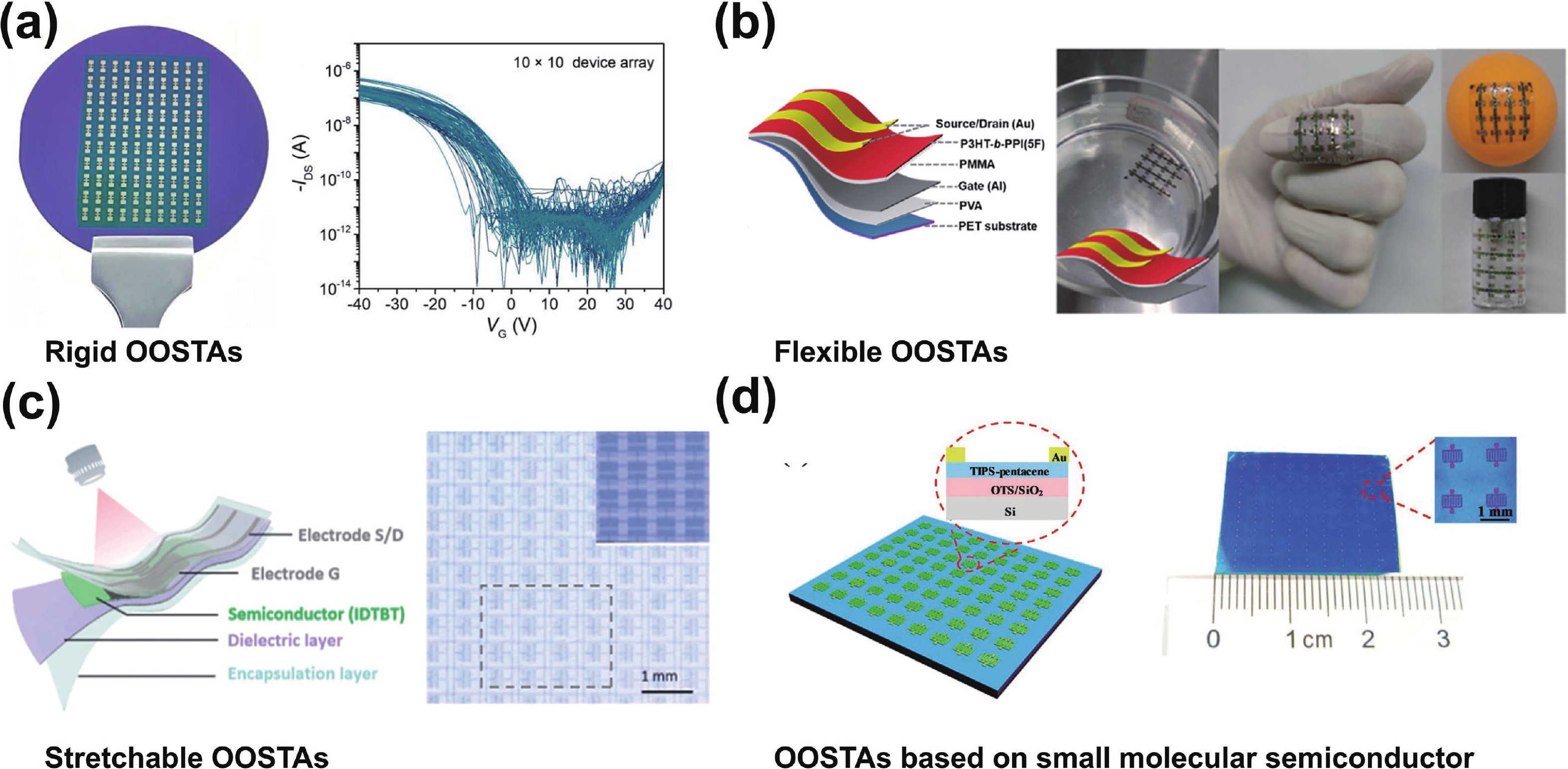
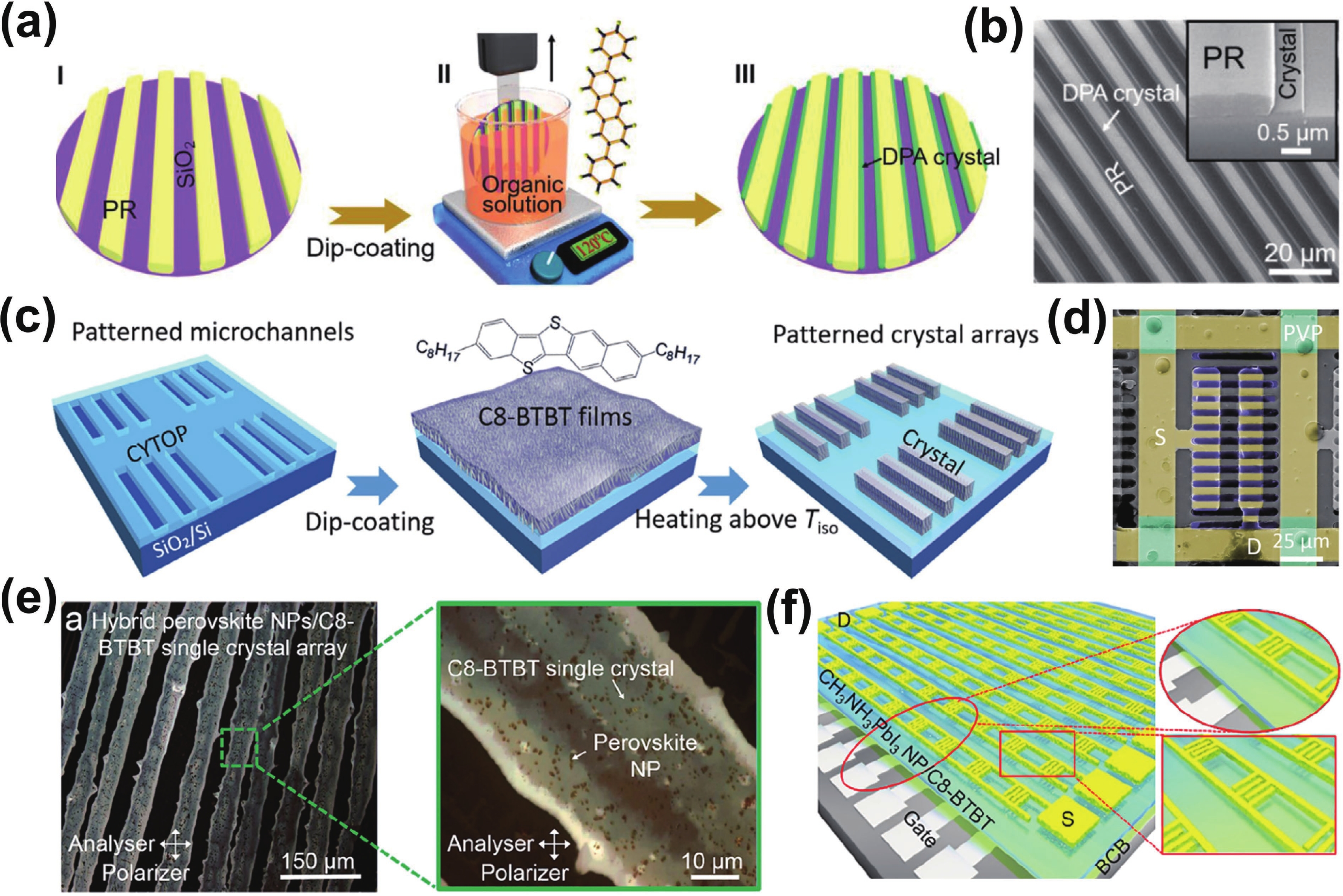
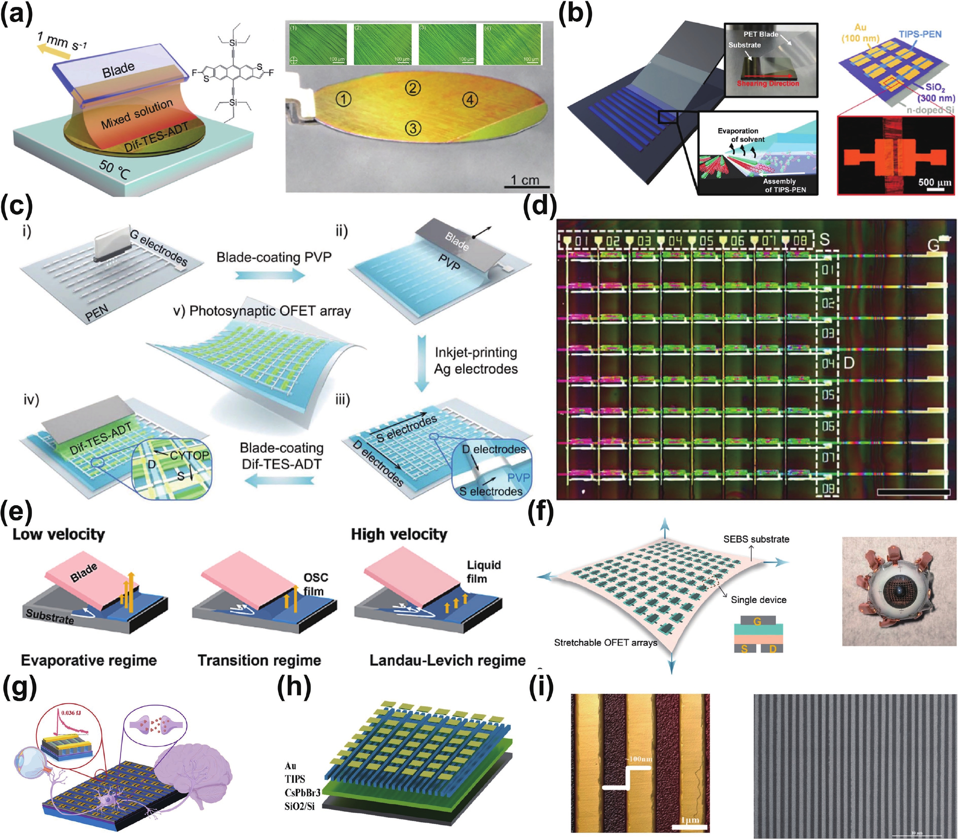
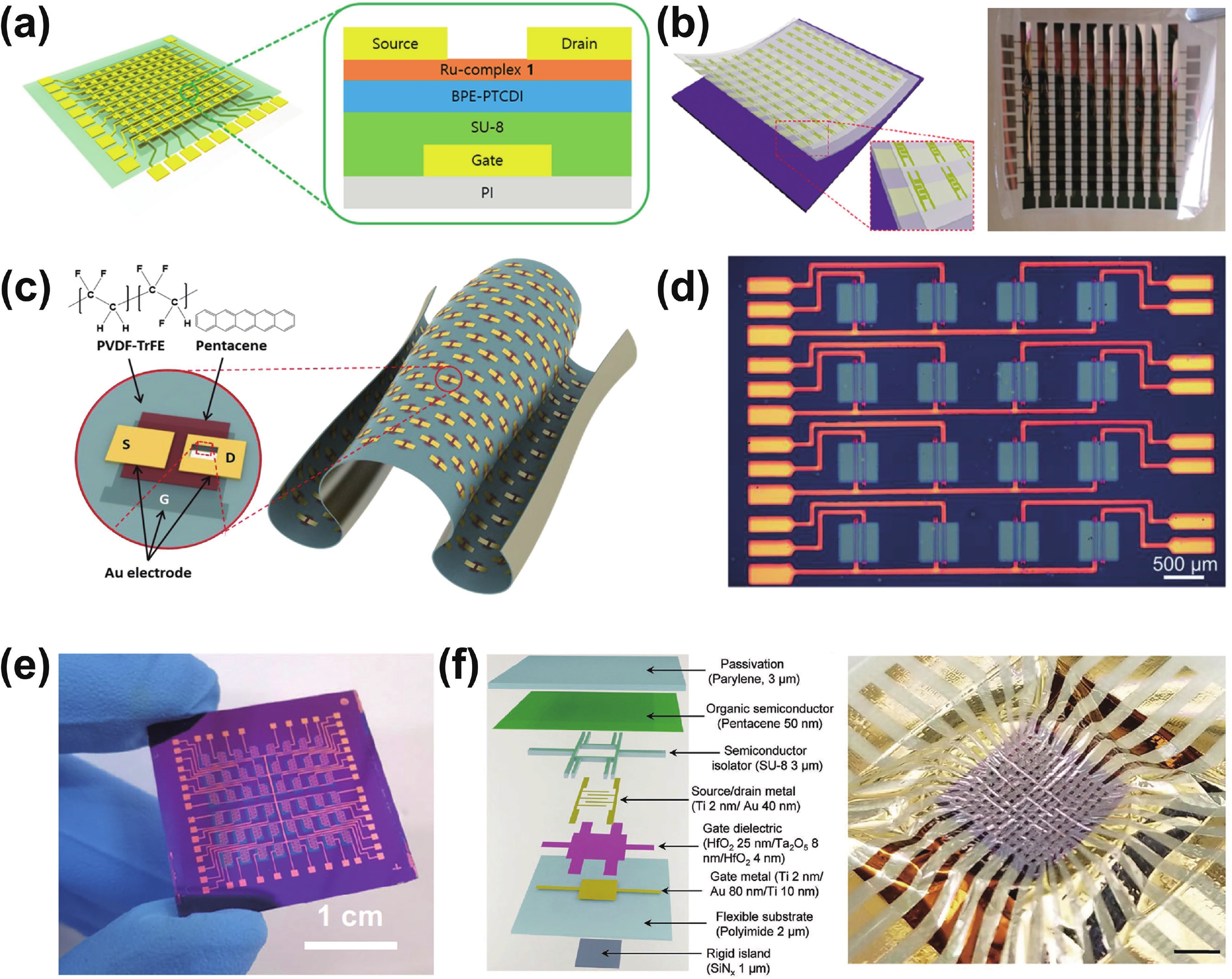
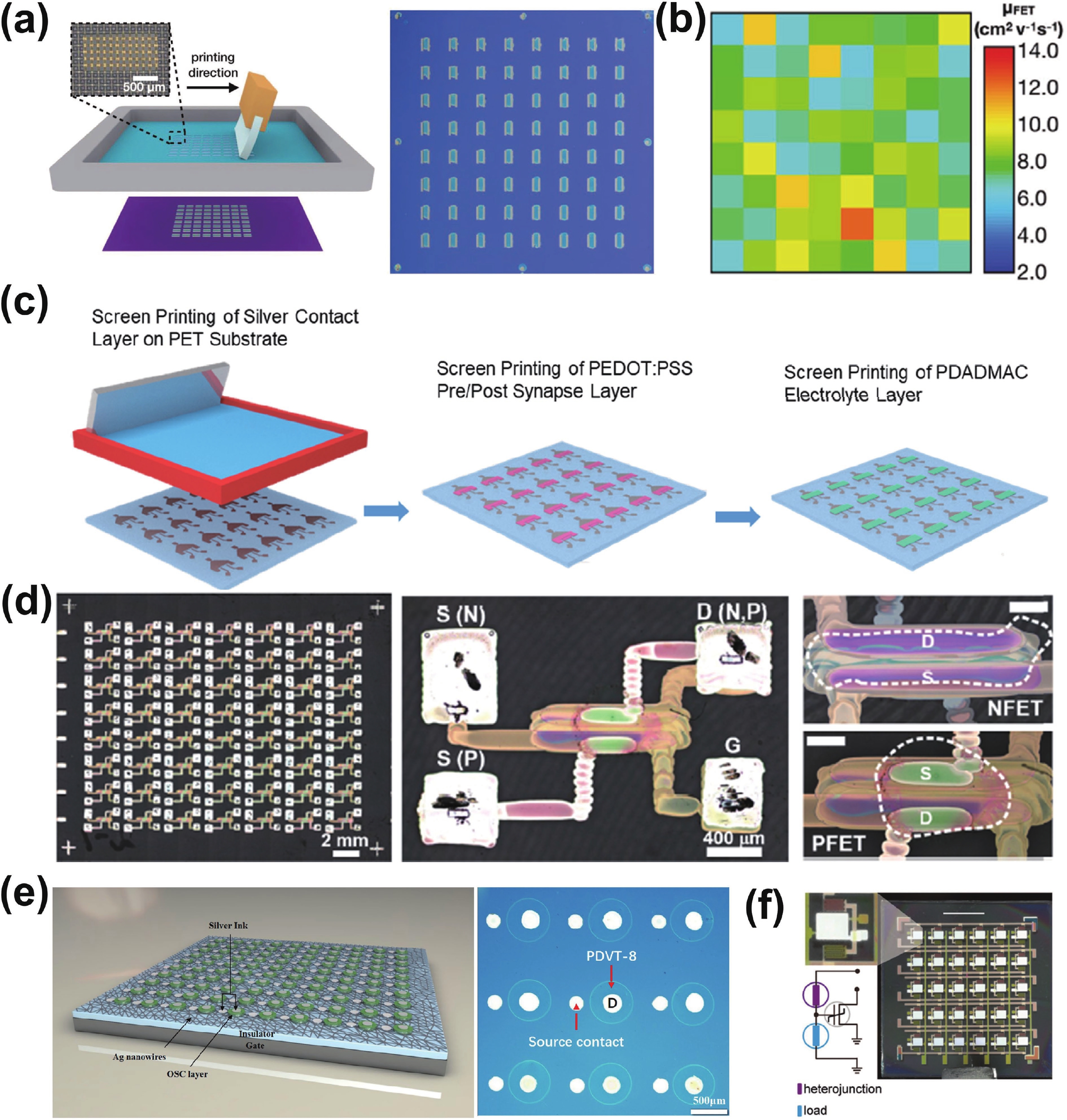
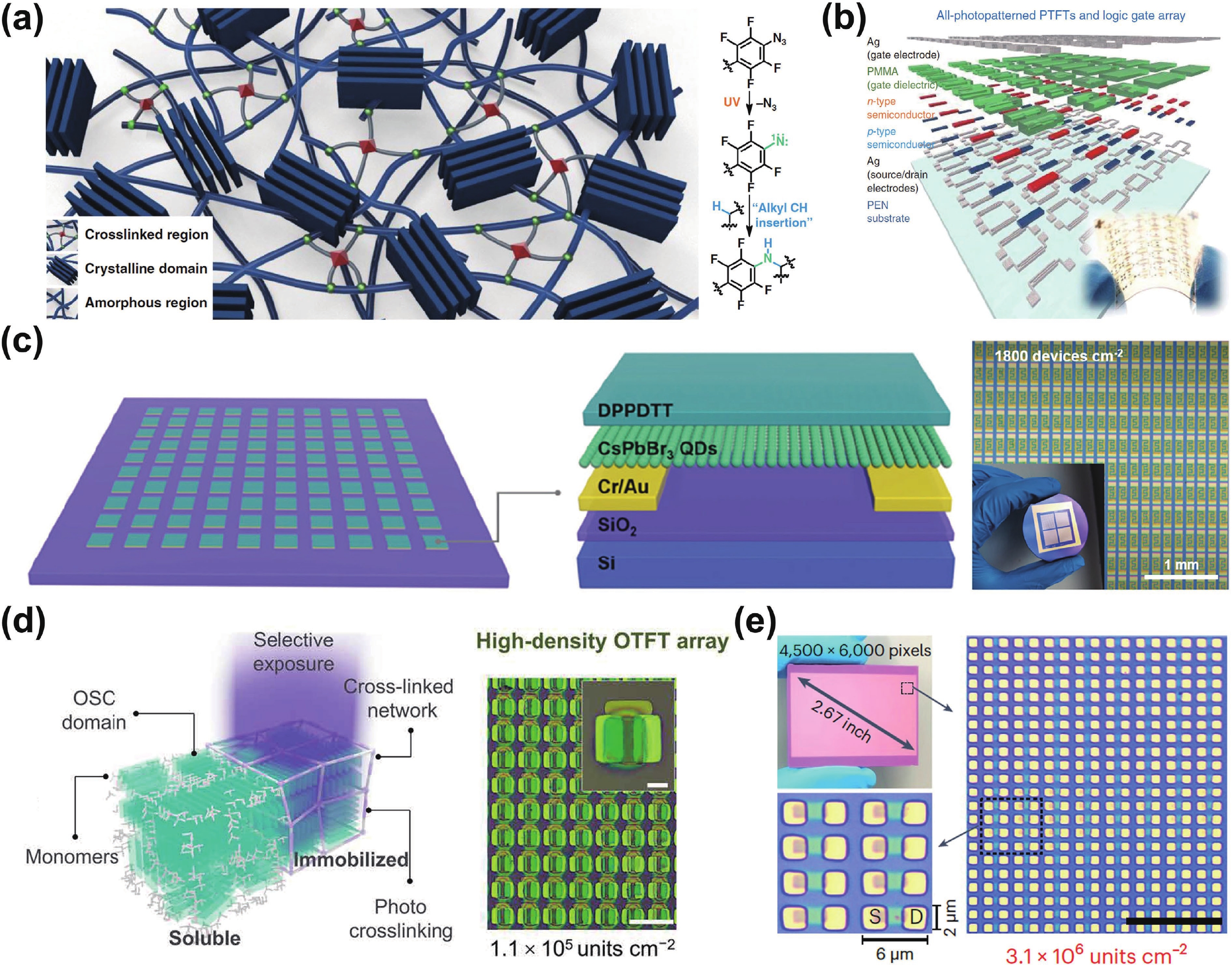
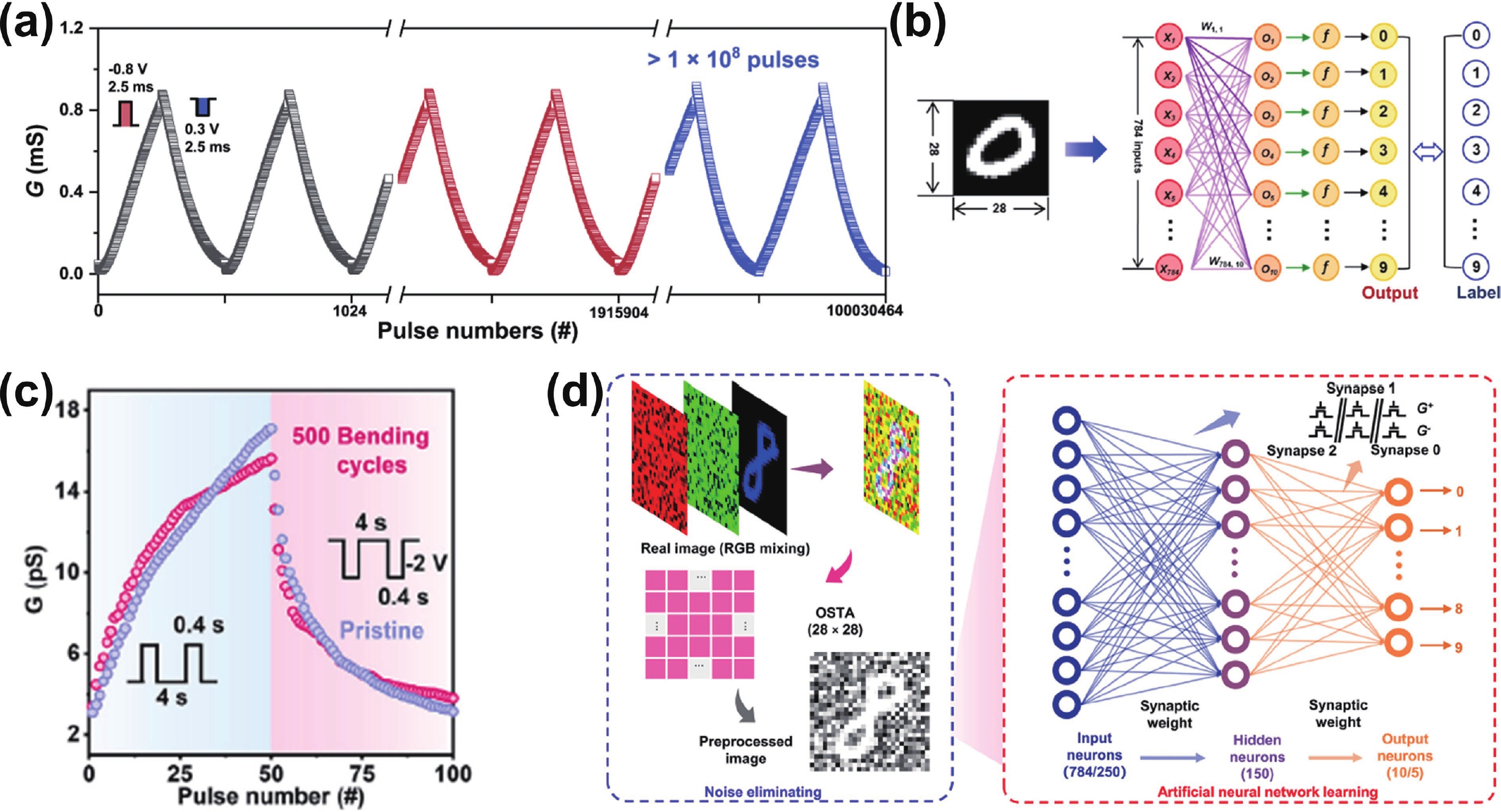
Table 1. Summary of the currently reported OOSTAs.
| Functional materials | Fabrication strategies of OOSTAs | Configuration of OOSTAs | Reference |
| DPPDTT/CsPbBr3 quantum dots | Spin coating | 6 × 6 | 31 |
| DPPDTT/Cl-HABI | Spin coating | 10 × 10 | 32 |
| P3HT-b-PPI(5F) | Spin coating | 4 × 4 | 33 |
| IDTBT | Spin coating | 4 × 4 | 34 |
| TIPS-pentacene | Spin coating | 9 × 8 | 35 |
| 2,6-diphenylanthracene (DPA) | Dip coating | 7 × 9 | 38 |
| C8-BTBT | Dip coating | 13 × 13 | 39 |
| CH3NH3PbI/C8-BTBT | Dip coating | 10 × 10 | 40 |
| Dif-TES-ADT | Blade coating | 5 × 8 | 42 |
| TES-ADT/PS | Blade coating | 8 × 8 | 44 |
| PDBT-co-TT/SEBS | Blade coating | 10 × 10 | 45 |
| TIPS-PEN/CsPbBr3/PVP | Drop casting | 4 × 4 | 46 |
| TIPS-PEN | Drop casting | 8 × 8 | 47 |
| TIPS-PEN | PVD | 4 × 4 | 52 |
| Pentacene | PVD | NA | 53 |
| 2-hexylthieno[4,5-b][1] benzothieno[3,2-b][1] benzothiophene | PVD | 8 × 6 | 54 |
| Pentacene | PVD | 12 × 12 | 55 |
| C8-BTBT/PMMA | Screen printing | 8 × 8 | 60 |
| PDVT-8 | Inkjet printing | NA | 63 |
| PVDT-10 | Inkjet printing | 5 × 6 | 64 |
| CsPbBr3 quantum dots/DPPDTT | Photolithography | up to 6500 units cm−2 | 69 |
| Poly(tetrathienoacene–diketopyrrolopyrrole)/CsPbBr3 | Photolithography | up to 3.1 × 10⁶ units cm−2 | 76 |
| CsPbBr3 quantum dots/DPPDTT | Photolithography | up to 6500 units cm−2 | 48 |
 DownLoad: CSV
| [1] |
Sun Z, Kvatinsky S, Si X, et al. A full spectrum of computing-in-memory technologies. Nat Electron, 2023, 6, 823 doi: 10.1038/s41928-023-01053-4
|
| [2] |
van de Burgt Y, Melianas A, Keene S T, et al. Organic electronics for neuromorphic computing. Nat Electron, 2018, 1, 386 doi: 10.1038/s41928-018-0103-3
|
| [3] |
Krestinskaya O, Fouda M E, Benmeziane H, et al. Neural architecture search for in-memory computing-based deep learning accelerators. Nat Rev Electr Eng, 2024, 1, 374 doi: 10.1038/s44287-024-00052-7
|
| [4] |
Aguirre F, Sebastian A, Le Gallo M, et al. Hardware implementation of memristor-based artificial neural networks. Nat Commun, 2024, 15(1), 1974 doi: 10.1038/s41467-024-45670-9
|
| [5] |
Zidan M A, Strachan J P, Lu W D. The future of electronics based on memristive systems. Nat Electron, 2018, 1, 22 doi: 10.1038/s41928-017-0006-8
|
| [6] |
Chen J W, Zhou Z, Kim B J, et al. Optoelectronic graded neurons for bioinspired in-sensor motion perception. Nat Nanotechnol, 2023, 18, 882 doi: 10.1038/s41565-023-01379-2
|
| [7] |
Zhang W Q, Gao B, Tang J S, et al. Neuro-inspired computing chips. Nat Electron, 2020, 3, 371 doi: 10.1038/s41928-020-0435-7
|
| [8] |
Zhou F C, Chai Y. Near-sensor and in-sensor computing. Nat Electron, 2020, 3, 664 doi: 10.1038/s41928-020-00501-9
|
| [9] |
Ren Q Q, Zhu C Y, Ma S J, et al. Optoelectronic devices for in-sensor computing. Adv Mater, 2024, e2407476 doi: 10.1002/adma.202407476
|
| [10] |
Wang Z Q, Wan T Q, Ma S J, et al. Multidimensional vision sensors for information processing. Nat Nanotechnol, 2024, 19, 919 doi: 10.1038/s41565-024-01665-7
|
| [11] |
Wang Y, Yin L, Huang W, et al. Optoelectronic synaptic devices for neuromorphic computing. Adv Intell Syst, 2021, 3, 2000099 doi: 10.1002/aisy.202000099
|
| [12] |
Schuman C D, Kulkarni S R, Parsa M, et al. Opportunities for neuromorphic computing algorithms and applications. Nat Comput Sci, 2022, 2, 10 doi: 10.1038/s43588-021-00184-y
|
| [13] |
Cho S W, Kwon S M, Kim Y H, et al. Recent progress in transistor-based optoelectronic synapses: From neuromorphic computing to artificial sensory system. Adv Intell Syst, 2021, 3, 2000162 doi: 10.1002/aisy.202000162
|
| [14] |
Wan Q Z, Sharbati M T, Erickson J R, et al. Emerging artificial synaptic devices for neuromorphic computing. Adv Mater Technol, 2019, 4, 1900037 doi: 10.1002/admt.201900037
|
| [15] |
Wang X, Ran Y X, Li X Q, et al. Bio-inspired artificial synaptic transistors: Evolution from innovative basic units to system integration. Mater Horiz, 2023, 10, 3269 doi: 10.1039/D3MH00216K
|
| [16] |
He Z H, Shen H G, Ye D K, et al. An organic transistor with light intensity-dependent active photoadaptation. Nat Electron, 2021, 4, 522 doi: 10.1038/s41928-021-00615-8
|
| [17] |
Choi Y, Oh S, Qian C, et al. Vertical organic synapse expandable to 3D crossbar array. Nat Commun, 2020, 11, 4595 doi: 10.1038/s41467-020-17850-w
|
| [18] |
Bu X B, Xu H, Shang D S, et al. Ion-gated transistor: An enabler for sensing and computing integration. Adv Intell Syst, 2020, 2, 2000156 doi: 10.1002/aisy.202000156
|
| [19] |
Li H L, Jiang X T, Ye W B, et al. Fully photon modulated heterostructure for neuromorphic computing. Nano Energy, 2019, 65, 104000 doi: 10.1016/j.nanoen.2019.104000
|
| [20] |
Xiao X Y, Hu J, Tang S, et al. Recent advances in halide perovskite memristors: Materials, structures, mechanisms, and applications. Adv Mater Technol, 2020, 5, 1900914 doi: 10.1002/admt.201900914
|
| [21] |
Duan X G, Cao Z L, Gao K K, et al. Memristor-based neuromorphic chips. Adv Mater, 2024, 36, 2310704 doi: 10.1002/adma.202310704
|
| [22] |
Sarwat S G, Kersting B, Moraitis T, et al. Phase-change memtransistive synapses for mixed-plasticity neural computations. Nat Nanotechnol, 2022, 17, 507 doi: 10.1038/s41565-022-01095-3
|
| [23] |
Jeong B H, Park J, Kim D, et al. Visible light-sensitive artificial photonic synapse. Adv Opt Mater, 2024, 12, 2301652 doi: 10.1002/adom.202301652
|
| [24] |
Wang J, Ilyas N, Ren Y, et al. Technology and integration roadmap for optoelectronic memristor. Adv Mater, 2024, 36, e2307393 doi: 10.1002/adma.202307393
|
| [25] |
Bronstein H, Nielsen C B, Schroeder B C, et al. The role of chemical design in the performance of organic semiconductors. Nat Rev Chem, 2020, 4, 66 doi: 10.1038/s41570-019-0152-9
|
| [26] |
Fuller E J, Keene S T, Melianas A, et al. Parallel programming of an ionic floating-gate memory array for scalable neuromorphic computing. Science, 2019, 364, 570 doi: 10.1126/science.aaw5581
|
| [27] |
Zhang X J, Deng W, Jia R F, et al. Precise patterning of organic semiconductor crystals for integrated device applications. Small, 2019, 15, 1900332 doi: 10.1002/smll.201900332
|
| [28] |
Wang W C, Chi L F. Patterned growth of organic semiconductors for ultra-high resolution microelectronics and optoelectronics. Wearable Electron, 2024, 1, 91 doi: 10.1016/j.wees.2024.05.005
|
| [29] |
Emslie A G, Bonner F T, Peck L G. Flow of a viscous liquid on a rotating disk. J Appl Phys, 1958, 29, 858 doi: 10.1063/1.1723300
|
| [30] |
Sahu N, Parija B, Panigrahi S. Fundamental understanding and modeling of spin coating process: A review. Indian J Phys, 2009, 83, 493 doi: 10.1007/s12648-009-0009-z
|
| [31] |
Hao D D, Zhang J Y, Dai S L, et al. Perovskite/organic semiconductor-based photonic synaptic transistor for artificial visual system. ACS Appl Mater Interfaces, 2020, 12, 39487 doi: 10.1021/acsami.0c10851
|
| [32] |
Liu D, Zhang J, Shi Q, et al. Humidity/oxygen-insensitive organic synaptic transistors based on optical radical effect. Adv Mater, 2024, 36, e2305370 doi: 10.1002/adma.202305370
|
| [33] |
Jiang L L, Huang H, Zhang C, et al. One-step preparation of semiconductor/dielectric bilayer structures for the simulation of flexible bionic photonic synapses. ACS Appl Mater Interfaces, 2023, 15, 7227 doi: 10.1021/acsami.2c22223
|
| [34] |
Xu F, Zhang C, Zhao X L, et al. Intrinsically stretchable photonic synaptic transistors for retina-like visual image systems. J Mater Chem C, 2022, 10, 10586 doi: 10.1039/D2TC01775J
|
| [35] |
Wang S Y, Zhao X L, Tong Y H, et al. Directly spin coating a low-viscosity organic semiconductor solution onto hydrophobic surfaces: Toward high-performance solution-processable organic transistors. Adv Materials Inter, 2020, 7, 1901950 doi: 10.1002/admi.201901950
|
| [36] |
Wang C Q, Lu Z J, Deng W, et al. Precise patterning of single crystal arrays of organic semiconductors by a patterned microchannel dip-coating method for organic field-effect transistors. J Mater Chem C, 2021, 9, 5174 doi: 10.1039/D1TC00035G
|
| [37] |
Wang H, Deng W, Huang L M, et al. Precisely patterned growth of ultra-long single-crystalline organic microwire arrays for near-infrared photodetectors. ACS Appl Mater Interfaces, 2016, 8, 7912 doi: 10.1021/acsami.5b12190
|
| [38] |
Deng W, Zhang X J, Dong H L, et al. Channel-restricted meniscus self-assembly for uniformly aligned growth of single-crystal arrays of organic semiconductors. Mater Today, 2019, 24, 17 doi: 10.1016/j.mattod.2018.07.018
|
| [39] |
Deng W, Lv Y, Zhang X L, et al. High-resolution patterning of organic semiconductor single crystal arrays for high-integration organic field-effect transistors. Mater Today, 2020, 40, 82 doi: 10.1016/j.mattod.2020.06.004
|
| [40] |
Xu X Z, Deng W, Zhang X J, et al. Dual-band, high-performance phototransistors from hybrid perovskite and organic crystal array for secure communication applications. ACS Nano, 2019, 13, 5910 doi: 10.1021/acsnano.9b01734
|
| [41] |
Zhang X, Zhang H, Li S L, et al. Development and application of blade-coating technique in organic solar cells. Nano Res, 2023, 16, 11571 doi: 10.1007/s12274-023-5425-9
|
| [42] |
Zhang X L, Deng W, Lu B, et al. Fast deposition of an ultrathin, highly crystalline organic semiconductor film for high-performance transistors. Nanoscale Horiz, 2020, 5, 1096 doi: 10.1039/D0NH00096E
|
| [43] |
Kim K, Nam K, Li X L, et al. Programmed design of highly crystalline organic semiconductor patterns with uniaxial alignment via blade coating for high-performance organic field-effect transistors. ACS Appl Mater Interfaces, 2019, 11, 42403 doi: 10.1021/acsami.9b12765
|
| [44] |
Shi J L, Jie J S, Deng W, et al. A fully solution-printed photosynaptic transistor array with ultralow energy consumption for artificial-vision neural networks. Adv Mater, 2022, 34, 2200380 doi: 10.1002/adma.202200380
|
| [45] |
Li X X, Sabir A, Zhang X Y, et al. Highly stretchable and oriented wafer-scale semiconductor films for organic phototransistor arrays. ACS Appl Mater Interfaces, 2024, 16, 36678 doi: 10.1021/acsami.4c04349
|
| [46] |
Hong H Y, Yang Z X, Ye Y L, et al. Highly uniform organic nanowire synaptic arrays with excellent performance for associative memory. Chem Eng J, 2024, 492, 152244 doi: 10.1016/j.cej.2024.152244
|
| [47] |
Shen Z H, Yang Z X, Zhou Y Q, et al. Ultralow-power consumption photonic synapse transistors based on organic array films fabricated using a particular prepatterned-guided crystallizing strategy. J Mater Chem C, 2023, 11, 3213 doi: 10.1039/D2TC05125G
|
| [48] |
Guo P, Zhang J Y, Pu H Q, et al. Wafer-scale photolithographic fabrication of organic synaptic transistor arrays. Device, 2024, 2, 100409 doi: 10.1016/j.device.2024.100409
|
| [49] |
Dai S L, Wu X H, Liu D P, et al. Light-stimulated synaptic devices utilizing interfacial effect of organic field-effect transistors. ACS Appl Mater Interfaces, 2018, 10, 21472 doi: 10.1021/acsami.8b05036
|
| [50] |
Zhang C, Xu F, Zhao X L, et al. Natural polyelectrolyte-based ultraflexible photoelectric synaptic transistors for hemispherical high-sensitive neuromorphic imaging system. Nano Energy, 2022, 95, 107001 doi: 10.1016/j.nanoen.2022.107001
|
| [51] |
Liu X E, Lee E K, Kim D Y, et al. Flexible organic phototransistor array with enhanced responsivity via metal-ligand charge transfer. ACS Appl Mater Interfaces, 2016, 8, 7291 doi: 10.1021/acsami.5b11523
|
| [52] |
Guo H T, Guo J, Wang Y J, et al. An organic optoelectronic synapse with multilevel memory enabled by gate modulation. ACS Appl Mater Interfaces, 2024, 16, 66948 doi: 10.1021/acsami.3c19624
|
| [53] |
Jang S, Jang S, Lee E H, et al. Ultrathin conformable organic artificial synapse for wearable intelligent device applications. ACS Appl Mater Interfaces, 2019, 11, 1071 doi: 10.1021/acsami.8b12092
|
| [54] |
Jiang T, Wang Y R, Zheng Y S, et al. Tetrachromatic vision-inspired neuromorphic sensors with ultraweak ultraviolet detection. Nat Commun, 2023, 14, 2281 doi: 10.1038/s41467-023-37973-0
|
| [55] |
Kim Y, Zhu C X, Lee W Y, et al. A hemispherical image sensor array fabricated with organic photomemory transistors. Adv Mater, 2023, 35, e2203541 doi: 10.1002/adma.202203541
|
| [56] |
Sakorikar T, Mihaliak N, Krisnadi F, et al. A guide to printed stretchable conductors. Chem Rev, 2024, 124, 860 doi: 10.1021/acs.chemrev.3c00569
|
| [57] |
Liang K, Wang R, Ren H, et al. Printable coffee-ring structures for highly uniform all-oxide optoelectronic synaptic transistors. Adv Opt Mater, 2022, 10, 2201754. doi: 10.1002/adom.202201754
|
| [58] |
Sui N Z, Ji Y X, Li M, et al. Photoprogrammed multifunctional optoelectronic synaptic transistor arrays based on photosensitive polymer-sorted semiconducting single-walled carbon nanotubes for image recognition. Adv Sci, 2024, 11, e2401794 doi: 10.1002/advs.202401794
|
| [59] |
Shi Q Q, Liu D P, Hao D D, et al. Printable, ultralow-power ternary synaptic transistors for multifunctional information processing system. Nano Energy, 2021, 87, 106197 doi: 10.1016/j.nanoen.2021.106197
|
| [60] |
Duan S M, Gao X, Wang Y, et al. Scalable fabrication of highly crystalline organic semiconductor thin film by channel-restricted screen printing toward the low-cost fabrication of high-performance transistor arrays. Adv Mater, 2019, 31, e1807975 doi: 10.1002/adma.201807975
|
| [61] |
Liu Q Z, Liu Y H, Li J, et al. Fully printed all-solid-state organic flexible artificial synapse for neuromorphic computing. ACS Appl Mater Interfaces, 2019, 11, 16749 doi: 10.1021/acsami.9b00226
|
| [62] |
Kwon J, Takeda Y, Fukuda K, et al. Three-dimensional, inkjet-printed organic transistors and integrated circuits with 100% yield, high uniformity, and long-term stability. ACS Nano, 2016, 10, 10324 doi: 10.1021/acsnano.6b06041
|
| [63] |
Fang Y, Wu X M, Lan S Q, et al. Inkjet-printed vertical organic field-effect transistor arrays and their image sensors. ACS Appl Mater Interfaces, 2018, 10, 30587 doi: 10.1021/acsami.8b06625
|
| [64] |
Wang H L, Zhao Q, Ni Z J, et al. A ferroelectric/electrochemical modulated organic synapse for ultraflexible, artificial visual-perception system. Adv Mater, 2018, 30, e1803961 doi: 10.1002/adma.201803961
|
| [65] |
Zhao X L, Wang S Y, Ni Y P, et al. High-performance full-photolithographic top-contact conformable organic transistors for soft electronics. Adv Sci, 2021, 8, 2004050 doi: 10.1002/advs.202004050
|
| [66] |
Kim M J, Lee M, Min H, et al. Universal three-dimensional crosslinker for all-photopatterned electronics. Nat Commun, 2020, 11, 1520 doi: 10.1038/s41467-020-15181-4
|
| [67] |
Kahle F, Saller C, Köhler A, et al. Crosslinked semiconductor polymers for photovoltaic applications. Adv Energy Mater, 2017, 7, 1700306 doi: 10.1002/aenm.201700306
|
| [68] |
Kim M J, Ryu H S, Choi Y Y, et al. Completely foldable electronics based on homojunction polymer transistors and logics. Sci Adv, 2021, 7, eabg8169 doi: 10.1126/sciadv.abg8169
|
| [69] |
Wu Y, Dai S, Liu X, et al. Optical microlithography of perovskite quantum dots/organic semiconductor heterojunctions for neuromorphic photosensors. Adv Funct Mater, 2024, 34, 175 doi: 10.1002/adfm.202315175
|
| [70] |
Zheng Y Q, Liu Y X, Zhong D L, et al. Monolithic optical microlithography of high-density elastic circuits. Science, 2021, 373, 88 doi: 10.1126/science.abh3551
|
| [71] |
Wang B H, Huang W, Lee S, et al. Foundry-compatible high-resolution patterning of vertically phase-separated semiconducting films for ultraflexible organic electronics. Nat Commun, 2021, 12, 4937 doi: 10.1038/s41467-021-25059-8
|
| [72] |
Park H W, Choi K Y, Shin J, et al. Universal route to impart orthogonality to polymer semiconductors for sub-micrometer tandem electronics. Adv Mater, 2019, 31, 1901400 doi: 10.1002/adma.201901400
|
| [73] |
Freudenberg J, Jänsch D, Hinkel F, et al. Immobilization strategies for organic semiconducting conjugated polymers. Chem Rev, 2018, 118, 5598 doi: 10.1021/acs.chemrev.8b00063
|
| [74] |
Chen R Z, Wang X J, Li X, et al. A comprehensive nano-interpenetrating semiconducting photoresist toward all-photolithography organic electronics. Sci Adv, 2021, 7, eabg0659 doi: 10.1126/sciadv.abg0659
|
| [75] |
Chen R Z, Yan Y K, Wang X J, et al. Patterning an erosion-free polymeric semiconductor channel for reliable all-photolithography organic electronics. J Phys Chem Lett, 2022, 13, 7673 doi: 10.1021/acs.jpclett.2c01982
|
| [76] |
Zhang S, Chen R Z, Kong D R, et al. Photovoltaic nanocells for high-performance large-scale-integrated organic phototransistors. Nat Nanotechnol, 2024, 19, 1323 doi: 10.1038/s41565-024-01707-0
|
| [77] |
Wang C Y, Bian Y S, Liu K, et al. Strain-insensitive viscoelastic perovskite film for intrinsically stretchable neuromorphic vision-adaptive transistors. Nat Commun, 2024, 15, 3123 doi: 10.1038/s41467-024-47532-w
|
| [78] |
Chen K, Hu H, Song I, et al. Organic optoelectronic synapse based on photon-modulated electrochemical doping. Nat Photonics, 2023, 17, 629 doi: 10.1038/s41566-023-01232-x
|
| [79] |
Dai S L, Dai Y H, Zhao Z X, et al. Intrinsically stretchable neuromorphic devices for on-body processing of health data with artificial intelligence. Matter, 2022, 5(10), 3375 doi: 10.1016/j.matt.2022.07.016
|
| [80] |
Guo P, Zhang J Y, Liu D P, et al. Optoelectronic synaptic transistors based on solution-processable organic semiconductors and CsPbCl3 quantum dots for visual nociceptor simulation and neuromorphic computing. ACS Appl Mater Interfaces, 2023, 15, 51483 doi: 10.1021/acsami.3c09355
|
| [81] |
Wang R Z, Chen P Y, Hao D D, et al. Artificial synapses based on lead-free perovskite floating-gate organic field-effect transistors for supervised and unsupervised learning. ACS Appl Mater Interfaces, 2021, 13, 43144 doi: 10.1021/acsami.1c08424
|
| [82] |
Lee Y, Park H L, Kim Y, et al. Organic electronic synapses with low energy consumption. Joule, 2021, 5, 794 doi: 10.1016/j.joule.2021.01.005
|


Article views: 2568 Times PDF downloads: 204 Times Cited by: 0 Times
Received: 14 December 2024 Revised: 04 January 2025 Online: Accepted Manuscript: 15 January 2025Uncorrected proof: 17 January 2025Published: 15 February 2025
| Citation: |
Pu Guo, Junyao Zhang, Jia Huang. Recent progress in organic optoelectronic synaptic transistor arrays: fabrication strategies and innovative applications of system integration[J]. Journal of Semiconductors, 2025, 46(2): 021405. doi: 10.1088/1674-4926/24120017
****
P Guo, J Y Zhang, and J Huang, Recent progress in organic optoelectronic synaptic transistor arrays: fabrication strategies and innovative applications of system integration[J]. J. Semicond., 2025, 46(2), 021405 doi: 10.1088/1674-4926/24120017

|
 Pu Guo got his B.Sc. in materials science and engineering at Northeast Forestry University in 2020. Now he is a PhD student at Tongji University under the supervision of Prof. Jia Huang. His research focuses on organic neuromorphic device arrays
 Jia Huang is a professor of materials science and engineering at Tongji University in Shanghai, China. He received his B.Sc. in materials science and engineering at the University of Science and Technology of China, his M.Sc. in applied science at the College of William & Mary, USA, and his Ph.D. in materials science and engineering at Johns Hopkins University, USA. Currently, Prof. Jia Huang’s research focuses on organic semiconductors, neuromorphic devices, flexible electronics, chemical and biological sensors, and thin-film transistors
| [1] |
Sun Z, Kvatinsky S, Si X, et al. A full spectrum of computing-in-memory technologies. Nat Electron, 2023, 6, 823 doi: 10.1038/s41928-023-01053-4
|
| [2] |
van de Burgt Y, Melianas A, Keene S T, et al. Organic electronics for neuromorphic computing. Nat Electron, 2018, 1, 386 doi: 10.1038/s41928-018-0103-3
|
| [3] |
Krestinskaya O, Fouda M E, Benmeziane H, et al. Neural architecture search for in-memory computing-based deep learning accelerators. Nat Rev Electr Eng, 2024, 1, 374 doi: 10.1038/s44287-024-00052-7
|
| [4] |
Aguirre F, Sebastian A, Le Gallo M, et al. Hardware implementation of memristor-based artificial neural networks. Nat Commun, 2024, 15(1), 1974 doi: 10.1038/s41467-024-45670-9
|
| [5] |
Zidan M A, Strachan J P, Lu W D. The future of electronics based on memristive systems. Nat Electron, 2018, 1, 22 doi: 10.1038/s41928-017-0006-8
|
| [6] |
Chen J W, Zhou Z, Kim B J, et al. Optoelectronic graded neurons for bioinspired in-sensor motion perception. Nat Nanotechnol, 2023, 18, 882 doi: 10.1038/s41565-023-01379-2
|
| [7] |
Zhang W Q, Gao B, Tang J S, et al. Neuro-inspired computing chips. Nat Electron, 2020, 3, 371 doi: 10.1038/s41928-020-0435-7
|
| [8] |
Zhou F C, Chai Y. Near-sensor and in-sensor computing. Nat Electron, 2020, 3, 664 doi: 10.1038/s41928-020-00501-9
|
| [9] |
Ren Q Q, Zhu C Y, Ma S J, et al. Optoelectronic devices for in-sensor computing. Adv Mater, 2024, e2407476 doi: 10.1002/adma.202407476
|
| [10] |
Wang Z Q, Wan T Q, Ma S J, et al. Multidimensional vision sensors for information processing. Nat Nanotechnol, 2024, 19, 919 doi: 10.1038/s41565-024-01665-7
|
| [11] |
Wang Y, Yin L, Huang W, et al. Optoelectronic synaptic devices for neuromorphic computing. Adv Intell Syst, 2021, 3, 2000099 doi: 10.1002/aisy.202000099
|
| [12] |
Schuman C D, Kulkarni S R, Parsa M, et al. Opportunities for neuromorphic computing algorithms and applications. Nat Comput Sci, 2022, 2, 10 doi: 10.1038/s43588-021-00184-y
|
| [13] |
Cho S W, Kwon S M, Kim Y H, et al. Recent progress in transistor-based optoelectronic synapses: From neuromorphic computing to artificial sensory system. Adv Intell Syst, 2021, 3, 2000162 doi: 10.1002/aisy.202000162
|
| [14] |
Wan Q Z, Sharbati M T, Erickson J R, et al. Emerging artificial synaptic devices for neuromorphic computing. Adv Mater Technol, 2019, 4, 1900037 doi: 10.1002/admt.201900037
|
| [15] |
Wang X, Ran Y X, Li X Q, et al. Bio-inspired artificial synaptic transistors: Evolution from innovative basic units to system integration. Mater Horiz, 2023, 10, 3269 doi: 10.1039/D3MH00216K
|
| [16] |
He Z H, Shen H G, Ye D K, et al. An organic transistor with light intensity-dependent active photoadaptation. Nat Electron, 2021, 4, 522 doi: 10.1038/s41928-021-00615-8
|
| [17] |
Choi Y, Oh S, Qian C, et al. Vertical organic synapse expandable to 3D crossbar array. Nat Commun, 2020, 11, 4595 doi: 10.1038/s41467-020-17850-w
|
| [18] |
Bu X B, Xu H, Shang D S, et al. Ion-gated transistor: An enabler for sensing and computing integration. Adv Intell Syst, 2020, 2, 2000156 doi: 10.1002/aisy.202000156
|
| [19] |
Li H L, Jiang X T, Ye W B, et al. Fully photon modulated heterostructure for neuromorphic computing. Nano Energy, 2019, 65, 104000 doi: 10.1016/j.nanoen.2019.104000
|
| [20] |
Xiao X Y, Hu J, Tang S, et al. Recent advances in halide perovskite memristors: Materials, structures, mechanisms, and applications. Adv Mater Technol, 2020, 5, 1900914 doi: 10.1002/admt.201900914
|
| [21] |
Duan X G, Cao Z L, Gao K K, et al. Memristor-based neuromorphic chips. Adv Mater, 2024, 36, 2310704 doi: 10.1002/adma.202310704
|
| [22] |
Sarwat S G, Kersting B, Moraitis T, et al. Phase-change memtransistive synapses for mixed-plasticity neural computations. Nat Nanotechnol, 2022, 17, 507 doi: 10.1038/s41565-022-01095-3
|
| [23] |
Jeong B H, Park J, Kim D, et al. Visible light-sensitive artificial photonic synapse. Adv Opt Mater, 2024, 12, 2301652 doi: 10.1002/adom.202301652
|
| [24] |
Wang J, Ilyas N, Ren Y, et al. Technology and integration roadmap for optoelectronic memristor. Adv Mater, 2024, 36, e2307393 doi: 10.1002/adma.202307393
|
| [25] |
Bronstein H, Nielsen C B, Schroeder B C, et al. The role of chemical design in the performance of organic semiconductors. Nat Rev Chem, 2020, 4, 66 doi: 10.1038/s41570-019-0152-9
|
| [26] |
Fuller E J, Keene S T, Melianas A, et al. Parallel programming of an ionic floating-gate memory array for scalable neuromorphic computing. Science, 2019, 364, 570 doi: 10.1126/science.aaw5581
|
| [27] |
Zhang X J, Deng W, Jia R F, et al. Precise patterning of organic semiconductor crystals for integrated device applications. Small, 2019, 15, 1900332 doi: 10.1002/smll.201900332
|
| [28] |
Wang W C, Chi L F. Patterned growth of organic semiconductors for ultra-high resolution microelectronics and optoelectronics. Wearable Electron, 2024, 1, 91 doi: 10.1016/j.wees.2024.05.005
|
| [29] |
Emslie A G, Bonner F T, Peck L G. Flow of a viscous liquid on a rotating disk. J Appl Phys, 1958, 29, 858 doi: 10.1063/1.1723300
|
| [30] |
Sahu N, Parija B, Panigrahi S. Fundamental understanding and modeling of spin coating process: A review. Indian J Phys, 2009, 83, 493 doi: 10.1007/s12648-009-0009-z
|
| [31] |
Hao D D, Zhang J Y, Dai S L, et al. Perovskite/organic semiconductor-based photonic synaptic transistor for artificial visual system. ACS Appl Mater Interfaces, 2020, 12, 39487 doi: 10.1021/acsami.0c10851
|
| [32] |
Liu D, Zhang J, Shi Q, et al. Humidity/oxygen-insensitive organic synaptic transistors based on optical radical effect. Adv Mater, 2024, 36, e2305370 doi: 10.1002/adma.202305370
|
| [33] |
Jiang L L, Huang H, Zhang C, et al. One-step preparation of semiconductor/dielectric bilayer structures for the simulation of flexible bionic photonic synapses. ACS Appl Mater Interfaces, 2023, 15, 7227 doi: 10.1021/acsami.2c22223
|
| [34] |
Xu F, Zhang C, Zhao X L, et al. Intrinsically stretchable photonic synaptic transistors for retina-like visual image systems. J Mater Chem C, 2022, 10, 10586 doi: 10.1039/D2TC01775J
|
| [35] |
Wang S Y, Zhao X L, Tong Y H, et al. Directly spin coating a low-viscosity organic semiconductor solution onto hydrophobic surfaces: Toward high-performance solution-processable organic transistors. Adv Materials Inter, 2020, 7, 1901950 doi: 10.1002/admi.201901950
|
| [36] |
Wang C Q, Lu Z J, Deng W, et al. Precise patterning of single crystal arrays of organic semiconductors by a patterned microchannel dip-coating method for organic field-effect transistors. J Mater Chem C, 2021, 9, 5174 doi: 10.1039/D1TC00035G
|
| [37] |
Wang H, Deng W, Huang L M, et al. Precisely patterned growth of ultra-long single-crystalline organic microwire arrays for near-infrared photodetectors. ACS Appl Mater Interfaces, 2016, 8, 7912 doi: 10.1021/acsami.5b12190
|
| [38] |
Deng W, Zhang X J, Dong H L, et al. Channel-restricted meniscus self-assembly for uniformly aligned growth of single-crystal arrays of organic semiconductors. Mater Today, 2019, 24, 17 doi: 10.1016/j.mattod.2018.07.018
|
| [39] |
Deng W, Lv Y, Zhang X L, et al. High-resolution patterning of organic semiconductor single crystal arrays for high-integration organic field-effect transistors. Mater Today, 2020, 40, 82 doi: 10.1016/j.mattod.2020.06.004
|
| [40] |
Xu X Z, Deng W, Zhang X J, et al. Dual-band, high-performance phototransistors from hybrid perovskite and organic crystal array for secure communication applications. ACS Nano, 2019, 13, 5910 doi: 10.1021/acsnano.9b01734
|
| [41] |
Zhang X, Zhang H, Li S L, et al. Development and application of blade-coating technique in organic solar cells. Nano Res, 2023, 16, 11571 doi: 10.1007/s12274-023-5425-9
|
| [42] |
Zhang X L, Deng W, Lu B, et al. Fast deposition of an ultrathin, highly crystalline organic semiconductor film for high-performance transistors. Nanoscale Horiz, 2020, 5, 1096 doi: 10.1039/D0NH00096E
|
| [43] |
Kim K, Nam K, Li X L, et al. Programmed design of highly crystalline organic semiconductor patterns with uniaxial alignment via blade coating for high-performance organic field-effect transistors. ACS Appl Mater Interfaces, 2019, 11, 42403 doi: 10.1021/acsami.9b12765
|
| [44] |
Shi J L, Jie J S, Deng W, et al. A fully solution-printed photosynaptic transistor array with ultralow energy consumption for artificial-vision neural networks. Adv Mater, 2022, 34, 2200380 doi: 10.1002/adma.202200380
|
| [45] |
Li X X, Sabir A, Zhang X Y, et al. Highly stretchable and oriented wafer-scale semiconductor films for organic phototransistor arrays. ACS Appl Mater Interfaces, 2024, 16, 36678 doi: 10.1021/acsami.4c04349
|
| [46] |
Hong H Y, Yang Z X, Ye Y L, et al. Highly uniform organic nanowire synaptic arrays with excellent performance for associative memory. Chem Eng J, 2024, 492, 152244 doi: 10.1016/j.cej.2024.152244
|
| [47] |
Shen Z H, Yang Z X, Zhou Y Q, et al. Ultralow-power consumption photonic synapse transistors based on organic array films fabricated using a particular prepatterned-guided crystallizing strategy. J Mater Chem C, 2023, 11, 3213 doi: 10.1039/D2TC05125G
|
| [48] |
Guo P, Zhang J Y, Pu H Q, et al. Wafer-scale photolithographic fabrication of organic synaptic transistor arrays. Device, 2024, 2, 100409 doi: 10.1016/j.device.2024.100409
|
| [49] |
Dai S L, Wu X H, Liu D P, et al. Light-stimulated synaptic devices utilizing interfacial effect of organic field-effect transistors. ACS Appl Mater Interfaces, 2018, 10, 21472 doi: 10.1021/acsami.8b05036
|
| [50] |
Zhang C, Xu F, Zhao X L, et al. Natural polyelectrolyte-based ultraflexible photoelectric synaptic transistors for hemispherical high-sensitive neuromorphic imaging system. Nano Energy, 2022, 95, 107001 doi: 10.1016/j.nanoen.2022.107001
|
| [51] |
Liu X E, Lee E K, Kim D Y, et al. Flexible organic phototransistor array with enhanced responsivity via metal-ligand charge transfer. ACS Appl Mater Interfaces, 2016, 8, 7291 doi: 10.1021/acsami.5b11523
|
| [52] |
Guo H T, Guo J, Wang Y J, et al. An organic optoelectronic synapse with multilevel memory enabled by gate modulation. ACS Appl Mater Interfaces, 2024, 16, 66948 doi: 10.1021/acsami.3c19624
|
| [53] |
Jang S, Jang S, Lee E H, et al. Ultrathin conformable organic artificial synapse for wearable intelligent device applications. ACS Appl Mater Interfaces, 2019, 11, 1071 doi: 10.1021/acsami.8b12092
|
| [54] |
Jiang T, Wang Y R, Zheng Y S, et al. Tetrachromatic vision-inspired neuromorphic sensors with ultraweak ultraviolet detection. Nat Commun, 2023, 14, 2281 doi: 10.1038/s41467-023-37973-0
|
| [55] |
Kim Y, Zhu C X, Lee W Y, et al. A hemispherical image sensor array fabricated with organic photomemory transistors. Adv Mater, 2023, 35, e2203541 doi: 10.1002/adma.202203541
|
| [56] |
Sakorikar T, Mihaliak N, Krisnadi F, et al. A guide to printed stretchable conductors. Chem Rev, 2024, 124, 860 doi: 10.1021/acs.chemrev.3c00569
|
| [57] |
Liang K, Wang R, Ren H, et al. Printable coffee-ring structures for highly uniform all-oxide optoelectronic synaptic transistors. Adv Opt Mater, 2022, 10, 2201754. doi: 10.1002/adom.202201754
|
| [58] |
Sui N Z, Ji Y X, Li M, et al. Photoprogrammed multifunctional optoelectronic synaptic transistor arrays based on photosensitive polymer-sorted semiconducting single-walled carbon nanotubes for image recognition. Adv Sci, 2024, 11, e2401794 doi: 10.1002/advs.202401794
|
| [59] |
Shi Q Q, Liu D P, Hao D D, et al. Printable, ultralow-power ternary synaptic transistors for multifunctional information processing system. Nano Energy, 2021, 87, 106197 doi: 10.1016/j.nanoen.2021.106197
|
| [60] |
Duan S M, Gao X, Wang Y, et al. Scalable fabrication of highly crystalline organic semiconductor thin film by channel-restricted screen printing toward the low-cost fabrication of high-performance transistor arrays. Adv Mater, 2019, 31, e1807975 doi: 10.1002/adma.201807975
|
| [61] |
Liu Q Z, Liu Y H, Li J, et al. Fully printed all-solid-state organic flexible artificial synapse for neuromorphic computing. ACS Appl Mater Interfaces, 2019, 11, 16749 doi: 10.1021/acsami.9b00226
|
| [62] |
Kwon J, Takeda Y, Fukuda K, et al. Three-dimensional, inkjet-printed organic transistors and integrated circuits with 100% yield, high uniformity, and long-term stability. ACS Nano, 2016, 10, 10324 doi: 10.1021/acsnano.6b06041
|
| [63] |
Fang Y, Wu X M, Lan S Q, et al. Inkjet-printed vertical organic field-effect transistor arrays and their image sensors. ACS Appl Mater Interfaces, 2018, 10, 30587 doi: 10.1021/acsami.8b06625
|
| [64] |
Wang H L, Zhao Q, Ni Z J, et al. A ferroelectric/electrochemical modulated organic synapse for ultraflexible, artificial visual-perception system. Adv Mater, 2018, 30, e1803961 doi: 10.1002/adma.201803961
|
| [65] |
Zhao X L, Wang S Y, Ni Y P, et al. High-performance full-photolithographic top-contact conformable organic transistors for soft electronics. Adv Sci, 2021, 8, 2004050 doi: 10.1002/advs.202004050
|
| [66] |
Kim M J, Lee M, Min H, et al. Universal three-dimensional crosslinker for all-photopatterned electronics. Nat Commun, 2020, 11, 1520 doi: 10.1038/s41467-020-15181-4
|
| [67] |
Kahle F, Saller C, Köhler A, et al. Crosslinked semiconductor polymers for photovoltaic applications. Adv Energy Mater, 2017, 7, 1700306 doi: 10.1002/aenm.201700306
|
| [68] |
Kim M J, Ryu H S, Choi Y Y, et al. Completely foldable electronics based on homojunction polymer transistors and logics. Sci Adv, 2021, 7, eabg8169 doi: 10.1126/sciadv.abg8169
|
| [69] |
Wu Y, Dai S, Liu X, et al. Optical microlithography of perovskite quantum dots/organic semiconductor heterojunctions for neuromorphic photosensors. Adv Funct Mater, 2024, 34, 175 doi: 10.1002/adfm.202315175
|
| [70] |
Zheng Y Q, Liu Y X, Zhong D L, et al. Monolithic optical microlithography of high-density elastic circuits. Science, 2021, 373, 88 doi: 10.1126/science.abh3551
|
| [71] |
Wang B H, Huang W, Lee S, et al. Foundry-compatible high-resolution patterning of vertically phase-separated semiconducting films for ultraflexible organic electronics. Nat Commun, 2021, 12, 4937 doi: 10.1038/s41467-021-25059-8
|
| [72] |
Park H W, Choi K Y, Shin J, et al. Universal route to impart orthogonality to polymer semiconductors for sub-micrometer tandem electronics. Adv Mater, 2019, 31, 1901400 doi: 10.1002/adma.201901400
|
| [73] |
Freudenberg J, Jänsch D, Hinkel F, et al. Immobilization strategies for organic semiconducting conjugated polymers. Chem Rev, 2018, 118, 5598 doi: 10.1021/acs.chemrev.8b00063
|
| [74] |
Chen R Z, Wang X J, Li X, et al. A comprehensive nano-interpenetrating semiconducting photoresist toward all-photolithography organic electronics. Sci Adv, 2021, 7, eabg0659 doi: 10.1126/sciadv.abg0659
|
| [75] |
Chen R Z, Yan Y K, Wang X J, et al. Patterning an erosion-free polymeric semiconductor channel for reliable all-photolithography organic electronics. J Phys Chem Lett, 2022, 13, 7673 doi: 10.1021/acs.jpclett.2c01982
|
| [76] |
Zhang S, Chen R Z, Kong D R, et al. Photovoltaic nanocells for high-performance large-scale-integrated organic phototransistors. Nat Nanotechnol, 2024, 19, 1323 doi: 10.1038/s41565-024-01707-0
|
| [77] |
Wang C Y, Bian Y S, Liu K, et al. Strain-insensitive viscoelastic perovskite film for intrinsically stretchable neuromorphic vision-adaptive transistors. Nat Commun, 2024, 15, 3123 doi: 10.1038/s41467-024-47532-w
|
| [78] |
Chen K, Hu H, Song I, et al. Organic optoelectronic synapse based on photon-modulated electrochemical doping. Nat Photonics, 2023, 17, 629 doi: 10.1038/s41566-023-01232-x
|
| [79] |
Dai S L, Dai Y H, Zhao Z X, et al. Intrinsically stretchable neuromorphic devices for on-body processing of health data with artificial intelligence. Matter, 2022, 5(10), 3375 doi: 10.1016/j.matt.2022.07.016
|
| [80] |
Guo P, Zhang J Y, Liu D P, et al. Optoelectronic synaptic transistors based on solution-processable organic semiconductors and CsPbCl3 quantum dots for visual nociceptor simulation and neuromorphic computing. ACS Appl Mater Interfaces, 2023, 15, 51483 doi: 10.1021/acsami.3c09355
|
| [81] |
Wang R Z, Chen P Y, Hao D D, et al. Artificial synapses based on lead-free perovskite floating-gate organic field-effect transistors for supervised and unsupervised learning. ACS Appl Mater Interfaces, 2021, 13, 43144 doi: 10.1021/acsami.1c08424
|
| [82] |
Lee Y, Park H L, Kim Y, et al. Organic electronic synapses with low energy consumption. Joule, 2021, 5, 794 doi: 10.1016/j.joule.2021.01.005
|

 WeChat ID
Journal of Semiconductors © 2017 All Rights Reserved 京ICP备05085259号-2


