


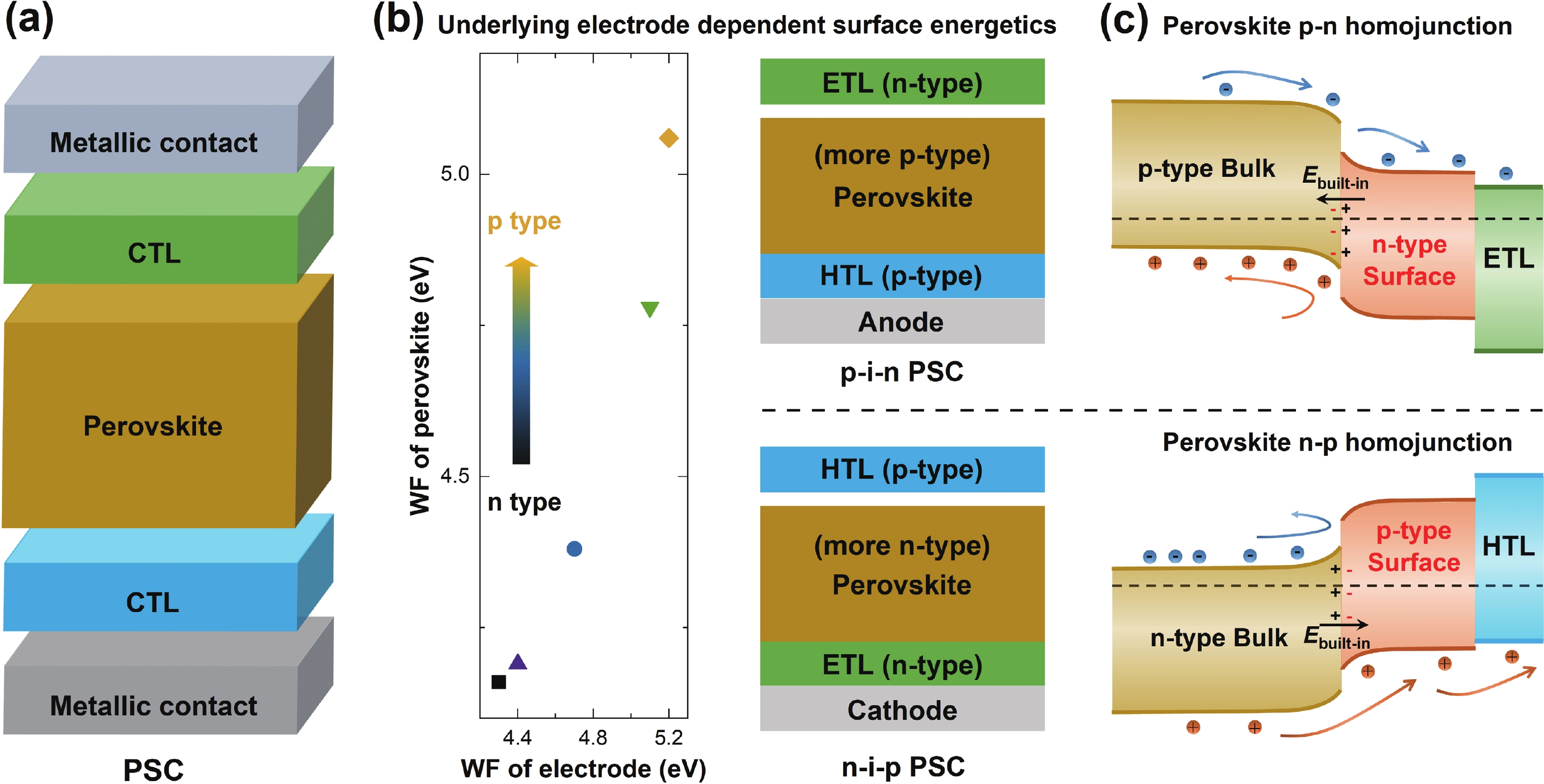
Fig. 1.
(Color online) Interface energetics in PSCs. (a) Device structure of PSCs. (b) Underlying electrode dependent perovskite surface energetics. (c) Constructing perovskite p−n (n−p) homojunction for p−i−n (n−i−p) PSCs.
COMMENTS AND OPINIONS
Shaobing Xiong1, Mats Fahlman2, and Qinye Bao1,
Corresponding author: Mats Fahlman, mats.fahlman@liu.se; Qinye Bao, qybao@clpm.ecnu.edu.cn
| [1] |
Stolterfoht M, Caprioglio P, Wolff CM, et al. The impact of energy alignment and interfacial recombination on the internal and external open-circuit voltage of perovskite solar cells. Energy Environ Sci, 2019, 12, 2778 doi: 10.1039/C9EE02020A
|
| [2] |
Yang J, Xiong S, Song J, et al. Energetics and energy loss in 2D Ruddlesden–Popper perovskite solar cells. Adv Energy Mater, 2020, 10, 2000687 doi: 10.1002/aenm.202000687
|
| [3] |
Tan S, Huang T, Yavuz I, et al. Stability-limiting heterointerfaces of perovskite photovoltaics. Nature, 2022, 605, 268 doi: 10.1038/s41586-022-04604-5
|
| [4] |
Xiong S, Dai Y, Yang J, et al. Surface charge-transfer doping for highly efficient perovskite solar cells. Nano Energy, 2021, 79, 105505 doi: 10.1016/j.nanoen.2020.105505
|
| [5] |
Miller EM, Zhao Y, Mercado CC, et al. Substrate-controlled band positions in CH3NH3PbI3 perovskite films. Phys Chem Chem Phys, 2014, 16, 22122 doi: 10.1039/C4CP03533J
|
| [6] |
Zohar A, Kulbak M, Levine I, et al. What limits the open-circuit voltage of bromide perovskite-based solar cells? ACS Energy Lett, 2019, 4, 1 doi: 10.1021/acsenergylett.8b01920
|
| [7] |
Schulz P, Cahen D, Kahn A. Halide perovskites: is it all about the interfaces? Chem Rev, 2019, 119, 3349 doi: 10.1021/acs.chemrev.8b00558
|
| [8] |
Li X, Zhang W, Guo X, et al. Constructing heterojunctions by surface sulfidation for efficient inverted perovskite solar cells. Science, 2022, 375, 434 doi: 10.1126/science.abl5676
|
| [9] |
Xiong S, Tian F, Wang F, et al. Reducing nonradiative recombination for highly efficient inverted perovskite solar cells via a synergistic bimolecular interface. Nat Commun, 2024, 15, 5607 doi: 10.1038/s41467-024-50019-3
|
| [10] |
Chen H, Maxwell A, Li C, et al. Regulating surface potential maximizes voltage in all-perovskite tandems. Nature, 2023, 613, 676 doi: 10.1038/s41586-022-05541-z
|
| [11] |
Xiong S, Chu J, Bao Q. Modulation of perovskite surface energetics for state-of-the-art solar cells. Sol RRL, 2023, 7, 2300458 doi: 10.1002/solr.202300458
|
| [12] |
Chu X, Ye Q, Wang Z, et al. Surface in situ reconstruction of inorganic perovskite films enabling long carrier lifetimes and solar cells with 21% efficiency. Nat Energy, 2023, 8, 372 doi: 10.1038/s41560-023-01220-z
|
| [13] |
Wu Y, Chang B, Wang L, et al. Intrinsic dipole arrangement to coordinate energy levels for efficient and stable perovskite solar cells. Adv Mater, 2023, 35, 2300174 doi: 10.1002/adma.202300174
|
| [14] |
Xiong S, Hou Z, Dong W, et al. Additive-induced synergies of defect passivation and energetic modification toward highly efficient perovskite solar cells. Adv Energy Mater, 2021, 11, 2101394 doi: 10.1002/aenm.202101394
|
| [15] |
Jiang S, Xiong S, Wu H, et al. In situ reconstruction of hole-selective perovskite heterojunction with graded energetics toward highly efficient and stable solar cells. Adv Energy Mater, 2023, 13, 2300983 doi: 10.1002/aenm.202300983
|
| [16] |
Xiong S, Hou Z, Zou S, et al. Direct observation on p- to n-type transformation of perovskite surface region during defect passivation driving high photovoltaic efficiency. Joule, 2021, 5, 467 doi: 10.1016/j.joule.2020.12.009
|
| [17] |
Wu Y, Yang X, Chen W, et al. Perovskite solar cells with 18.21% efficiency and area over 1 cm2 fabricated by heterojunction engineering. Nat Energy, 2016, 1, 16148 doi: 10.1038/nenergy.2016.148
|
| [18] |
Sidhik S, Wang Y, De Siena M, et al. Deterministic fabrication of 3D/2D perovskite bilayer stacks for durable and efficient solar cells. Science, 2022, 377, 1425 doi: 10.1126/science.abq7652
|
| [19] |
Ma K, Sun J, Atapattu HR, et al. Holistic energy landscape management in 2D/3D heterojunction via molecular engineering for efficient perovskite solar cells. Sci Adv, 2023, 9, eadg0032 doi: 10.1126/sciadv.adg0032
|
| [20] |
Zang X, Xiong S, Jiang S, et al. Passivating dipole layer bridged 3D/2D perovskite heterojunction for highly efficient and stable p-i-n solar cells. Adv Mater, 2024, 36, 2309991 doi: 10.1002/adma.202309991
|
| [21] |
Zhu C, Wang X, Liu W, et al. Organic interlayer materials for non-fullerene solar cells. Trends Chem, 2024, 3, 37 doi: 10.1016/j.trechm.2023.11.002
|
| [22] |
Zhang H, Li Y, Zhang X, et al. Role of interface properties in organic solar cells: from substrate engineering to bulk-heterojunction interfacial morphology. Mater Chem Front, 2020, 4, 2863 doi: 10.1039/D0QM00398K
|
| [23] |
Zhang Q, Liu T, Wilken S, et al. Industrial kraft lignin based binary cathode interface layer enables enhanced stability in high efficiency organic solar cells. Adv Mater, 2024, 36, 2307646 doi: 10.1002/adma.202307646
|
| [24] |
Wetzelaer G J A H, Blom P W M. Comment on "enhanced charge selectivity via anodic-C60 layer reduces nonradiative losses in organic solar cells". ACS Appl Mater Interfaces, 2022, 14, 7523 doi: 10.1021/acsami.1c05333
|
| [25] |
Fahlman M, Fabiano S, Gueskine V, et al. Interfaces in organic electronics. Nat Rev Mater, 2019, 4, 627 doi: 10.1038/s41578-019-0127-y
|
| [26] |
Nyman M, Ahläng C, Dahlström S, et al. Highly conductive charge transport layers impair charge extraction selectivity in thin-film solar cells. Adv Energy Sustainability Res, 2023, 4, 2300030 doi: 10.1002/aesr.202300030
|
| [27] |
Jing J, Dong S, Zhang K, et al. In-situ self-organized anode interlayer enables organic solar cells with simultaneously simplified processing and greatly improved efficiency to 17.8%. Nano Energy, 2022, 93, 106814 doi: 10.1016/j.nanoen.2021.106814
|
| [28] |
Liu T, Heimonen J, Zhang Q, et al. Ground-state electron transfer in all-polymer donor: acceptor blends enables aqueous processing of water-insoluble conjugated polymers. Nat Commun, 2023, 14, 8454 doi: 10.1038/s41467-023-44153-7
|
| [29] |
Sun L, Fukuda K, Someya T. Recent progress in solution-processed flexible organic photovoltaics. npj Flexible Electron, 2022, 6, 89 doi: 10.1038/s41528-022-00222-3
|
| [30] |
van Reenen S, Kouijzer S, Janssen RAJ, et al. Origin of work function modification by ionic and amine-based interface layers. Adv Mater Interfaces, 2014, 1, 1400189 doi: 10.1002/admi.201400189
|
| [31] |
Bao Q, Liu X, Wang E, et al. Regular energetics at conjugated electrolyte/electrode modifier for organic electronics and their implications on design rules. Adv Mater Interfaces, 2015, 2, 1500204 doi: 10.1002/admi.201500204
|
| [32] |
Cui Y, Jia G, Zhu J, et al. The critical role of anode work function in non-fullerene organic solar cells unveiled by counterion-size-controlled self-doping conjugated polymers. Chem Mater, 2018, 30, 1078 doi: 10.1021/acs.chemmater.7b04982
|
| [33] |
You Z, Song Y, Liu W, et al. Diazabicyclic electroactive ionenes for efficient and stable organic solar cells. Angew Chem, Int Ed, 2023, 62, e202302538 doi: 10.1002/anie.202302538
|
| [34] |
Lin Y, Zhang Y, Zhang J, et al. 18.9% efficient organic solar cells based on n-doped bulk-heterojunction and halogen-substituted self-assembled monolayers as hole extracting interlayers. Adv Energy Mater, 2022, 12, 2202503 doi: 10.1002/aenm.202202503
|
| [35] |
Zhang Q, Wang C, Liu X, et al. Understanding the work function modification by a self-assembled polyvinylpyrrolidone layer in inverted organic solar cells. Sol RRL, 2021, 5, 2000575 doi: 10.1002/solr.202000575
|
| [36] |
Li Q, Huang J D, Liu T, et al. A highly conductive n-type conjugated polymer synthesized in water. J Am Chem Soc, 2024, 146, 15860 doi: 10.1021/jacs.4c02270
|


Article views: 1483 Times PDF downloads: 107 Times Cited by: 0 Times
Received: 16 January 2025 Revised: Online: Accepted Manuscript: 08 February 2025Uncorrected proof: 18 February 2025Published: 15 May 2025
| Citation: |
Shaobing Xiong, Mats Fahlman, Qinye Bao. Interface energetics in organic and perovskite semiconductor solar cells[J]. Journal of Semiconductors, 2025, 46(5): 050301. doi: 10.1088/1674-4926/25010021
****
S B Xiong, M Fahlman, and Q Y Bao, Interface energetics in organic and perovskite semiconductor solar cells[J]. J. Semicond., 2025, 46(5), 050301 doi: 10.1088/1674-4926/25010021

|
 Shaobing Xiong is currently an associate professor in School of Physics and Electronic Science at East China Normal University. He received his B.S. in Physics from Soochow University in 2017 and Ph.D. in Physical Electronics from East China Normal University in 2022. His research focuses on the interface properties and photoelectric regulation of organic and perovskite optoelectronic devices
 Mats Fahlman received his M.S. in Engineering Physics (1991) and Ph.D. in Surface Physics and Chemistry (1995) from Linköping University, Sweden, where he is currently a full professor at the Laboratory of Organic Electronics. He is active in the research of organic semiconductors using primarily surface science techniques to explore materials and interfaces as well as their effect on device properties
 Qinye Bao is currently a professor in School of Physics and Electronic Science at East China Normal University. He received his Ph.D. in 2015 in Surface Physics and Chemistry from Linköping University, Sweden. The focus of his work is on surface science techniques, such as ultraviolet photoelectron spectroscopy, X-ray photoelectron spectroscopy, and near edge X-ray absorption fine structure spectroscopy, to reveal the relationship between interface electronic structures and device performance, especially for application in organic solar cells, organic light-emitting diodes, and perovskite-based optoelectronic devices
| [1] |
Stolterfoht M, Caprioglio P, Wolff CM, et al. The impact of energy alignment and interfacial recombination on the internal and external open-circuit voltage of perovskite solar cells. Energy Environ Sci, 2019, 12, 2778 doi: 10.1039/C9EE02020A
|
| [2] |
Yang J, Xiong S, Song J, et al. Energetics and energy loss in 2D Ruddlesden–Popper perovskite solar cells. Adv Energy Mater, 2020, 10, 2000687 doi: 10.1002/aenm.202000687
|
| [3] |
Tan S, Huang T, Yavuz I, et al. Stability-limiting heterointerfaces of perovskite photovoltaics. Nature, 2022, 605, 268 doi: 10.1038/s41586-022-04604-5
|
| [4] |
Xiong S, Dai Y, Yang J, et al. Surface charge-transfer doping for highly efficient perovskite solar cells. Nano Energy, 2021, 79, 105505 doi: 10.1016/j.nanoen.2020.105505
|
| [5] |
Miller EM, Zhao Y, Mercado CC, et al. Substrate-controlled band positions in CH3NH3PbI3 perovskite films. Phys Chem Chem Phys, 2014, 16, 22122 doi: 10.1039/C4CP03533J
|
| [6] |
Zohar A, Kulbak M, Levine I, et al. What limits the open-circuit voltage of bromide perovskite-based solar cells? ACS Energy Lett, 2019, 4, 1 doi: 10.1021/acsenergylett.8b01920
|
| [7] |
Schulz P, Cahen D, Kahn A. Halide perovskites: is it all about the interfaces? Chem Rev, 2019, 119, 3349 doi: 10.1021/acs.chemrev.8b00558
|
| [8] |
Li X, Zhang W, Guo X, et al. Constructing heterojunctions by surface sulfidation for efficient inverted perovskite solar cells. Science, 2022, 375, 434 doi: 10.1126/science.abl5676
|
| [9] |
Xiong S, Tian F, Wang F, et al. Reducing nonradiative recombination for highly efficient inverted perovskite solar cells via a synergistic bimolecular interface. Nat Commun, 2024, 15, 5607 doi: 10.1038/s41467-024-50019-3
|
| [10] |
Chen H, Maxwell A, Li C, et al. Regulating surface potential maximizes voltage in all-perovskite tandems. Nature, 2023, 613, 676 doi: 10.1038/s41586-022-05541-z
|
| [11] |
Xiong S, Chu J, Bao Q. Modulation of perovskite surface energetics for state-of-the-art solar cells. Sol RRL, 2023, 7, 2300458 doi: 10.1002/solr.202300458
|
| [12] |
Chu X, Ye Q, Wang Z, et al. Surface in situ reconstruction of inorganic perovskite films enabling long carrier lifetimes and solar cells with 21% efficiency. Nat Energy, 2023, 8, 372 doi: 10.1038/s41560-023-01220-z
|
| [13] |
Wu Y, Chang B, Wang L, et al. Intrinsic dipole arrangement to coordinate energy levels for efficient and stable perovskite solar cells. Adv Mater, 2023, 35, 2300174 doi: 10.1002/adma.202300174
|
| [14] |
Xiong S, Hou Z, Dong W, et al. Additive-induced synergies of defect passivation and energetic modification toward highly efficient perovskite solar cells. Adv Energy Mater, 2021, 11, 2101394 doi: 10.1002/aenm.202101394
|
| [15] |
Jiang S, Xiong S, Wu H, et al. In situ reconstruction of hole-selective perovskite heterojunction with graded energetics toward highly efficient and stable solar cells. Adv Energy Mater, 2023, 13, 2300983 doi: 10.1002/aenm.202300983
|
| [16] |
Xiong S, Hou Z, Zou S, et al. Direct observation on p- to n-type transformation of perovskite surface region during defect passivation driving high photovoltaic efficiency. Joule, 2021, 5, 467 doi: 10.1016/j.joule.2020.12.009
|
| [17] |
Wu Y, Yang X, Chen W, et al. Perovskite solar cells with 18.21% efficiency and area over 1 cm2 fabricated by heterojunction engineering. Nat Energy, 2016, 1, 16148 doi: 10.1038/nenergy.2016.148
|
| [18] |
Sidhik S, Wang Y, De Siena M, et al. Deterministic fabrication of 3D/2D perovskite bilayer stacks for durable and efficient solar cells. Science, 2022, 377, 1425 doi: 10.1126/science.abq7652
|
| [19] |
Ma K, Sun J, Atapattu HR, et al. Holistic energy landscape management in 2D/3D heterojunction via molecular engineering for efficient perovskite solar cells. Sci Adv, 2023, 9, eadg0032 doi: 10.1126/sciadv.adg0032
|
| [20] |
Zang X, Xiong S, Jiang S, et al. Passivating dipole layer bridged 3D/2D perovskite heterojunction for highly efficient and stable p-i-n solar cells. Adv Mater, 2024, 36, 2309991 doi: 10.1002/adma.202309991
|
| [21] |
Zhu C, Wang X, Liu W, et al. Organic interlayer materials for non-fullerene solar cells. Trends Chem, 2024, 3, 37 doi: 10.1016/j.trechm.2023.11.002
|
| [22] |
Zhang H, Li Y, Zhang X, et al. Role of interface properties in organic solar cells: from substrate engineering to bulk-heterojunction interfacial morphology. Mater Chem Front, 2020, 4, 2863 doi: 10.1039/D0QM00398K
|
| [23] |
Zhang Q, Liu T, Wilken S, et al. Industrial kraft lignin based binary cathode interface layer enables enhanced stability in high efficiency organic solar cells. Adv Mater, 2024, 36, 2307646 doi: 10.1002/adma.202307646
|
| [24] |
Wetzelaer G J A H, Blom P W M. Comment on "enhanced charge selectivity via anodic-C60 layer reduces nonradiative losses in organic solar cells". ACS Appl Mater Interfaces, 2022, 14, 7523 doi: 10.1021/acsami.1c05333
|
| [25] |
Fahlman M, Fabiano S, Gueskine V, et al. Interfaces in organic electronics. Nat Rev Mater, 2019, 4, 627 doi: 10.1038/s41578-019-0127-y
|
| [26] |
Nyman M, Ahläng C, Dahlström S, et al. Highly conductive charge transport layers impair charge extraction selectivity in thin-film solar cells. Adv Energy Sustainability Res, 2023, 4, 2300030 doi: 10.1002/aesr.202300030
|
| [27] |
Jing J, Dong S, Zhang K, et al. In-situ self-organized anode interlayer enables organic solar cells with simultaneously simplified processing and greatly improved efficiency to 17.8%. Nano Energy, 2022, 93, 106814 doi: 10.1016/j.nanoen.2021.106814
|
| [28] |
Liu T, Heimonen J, Zhang Q, et al. Ground-state electron transfer in all-polymer donor: acceptor blends enables aqueous processing of water-insoluble conjugated polymers. Nat Commun, 2023, 14, 8454 doi: 10.1038/s41467-023-44153-7
|
| [29] |
Sun L, Fukuda K, Someya T. Recent progress in solution-processed flexible organic photovoltaics. npj Flexible Electron, 2022, 6, 89 doi: 10.1038/s41528-022-00222-3
|
| [30] |
van Reenen S, Kouijzer S, Janssen RAJ, et al. Origin of work function modification by ionic and amine-based interface layers. Adv Mater Interfaces, 2014, 1, 1400189 doi: 10.1002/admi.201400189
|
| [31] |
Bao Q, Liu X, Wang E, et al. Regular energetics at conjugated electrolyte/electrode modifier for organic electronics and their implications on design rules. Adv Mater Interfaces, 2015, 2, 1500204 doi: 10.1002/admi.201500204
|
| [32] |
Cui Y, Jia G, Zhu J, et al. The critical role of anode work function in non-fullerene organic solar cells unveiled by counterion-size-controlled self-doping conjugated polymers. Chem Mater, 2018, 30, 1078 doi: 10.1021/acs.chemmater.7b04982
|
| [33] |
You Z, Song Y, Liu W, et al. Diazabicyclic electroactive ionenes for efficient and stable organic solar cells. Angew Chem, Int Ed, 2023, 62, e202302538 doi: 10.1002/anie.202302538
|
| [34] |
Lin Y, Zhang Y, Zhang J, et al. 18.9% efficient organic solar cells based on n-doped bulk-heterojunction and halogen-substituted self-assembled monolayers as hole extracting interlayers. Adv Energy Mater, 2022, 12, 2202503 doi: 10.1002/aenm.202202503
|
| [35] |
Zhang Q, Wang C, Liu X, et al. Understanding the work function modification by a self-assembled polyvinylpyrrolidone layer in inverted organic solar cells. Sol RRL, 2021, 5, 2000575 doi: 10.1002/solr.202000575
|
| [36] |
Li Q, Huang J D, Liu T, et al. A highly conductive n-type conjugated polymer synthesized in water. J Am Chem Soc, 2024, 146, 15860 doi: 10.1021/jacs.4c02270
|

 WeChat ID
Journal of Semiconductors © 2017 All Rights Reserved 京ICP备05085259号-2

 DownLoad:

