| Citation: |
Sudhansu Kumar Pati, Kalyan Koley, Arka Dutta, N Mohankumar, Chandan Kumar Sarkar. A new approach to extracting the RF parameters of asymmetric DG MOSFETs with the NQS effect[J]. Journal of Semiconductors, 2013, 34(11): 114002. doi: 10.1088/1674-4926/34/11/114002
****
S K Pati, K Koley, A Dutta, N Mohankumar, C K Sarkar. A new approach to extracting the RF parameters of asymmetric DG MOSFETs with the NQS effect[J]. J. Semicond., 2013, 34(11): 114002. doi: 10.1088/1674-4926/34/11/114002.
|
A new approach to extracting the RF parameters of asymmetric DG MOSFETs with the NQS effect
DOI: 10.1088/1674-4926/34/11/114002
More Information
-
Abstract
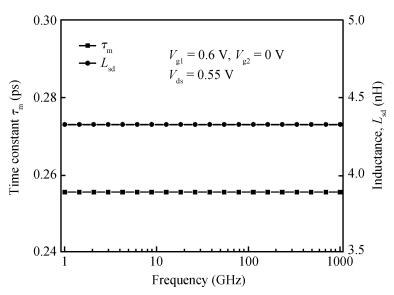
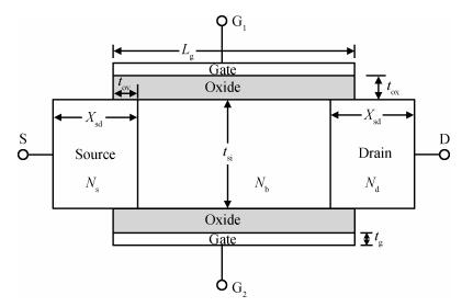
In analog circuit design an important parameter, from the perspective of superior device performance, is linearity. The DG MOSFET in asymmetric mode operation has been found to present a better linearity. In addition to that it provides, at the discretion of analog circuit designer, an additional degree of freedom, by providing independent bias control for the front and the back gates. Here a non-quasi-static (NQS) small signal model for DGMOSFET with asymmetric gate bias is proposed for extracting the parameters of the device using TCAD simulations. The parameters extracted here for analysis are the intrinsic front and back gate to drain capacitance, Cgd1 and Cgd2, the intrinsic front and back distributed channel resistance, Rgd1 and Rgd2 respectively, the transport delay, τm, and the inductance, Lsd. The parameter extraction model for an asymmetric DG MOSFET is validated with pre-established extracted parameter data, for symmetric DG MOSFET devices, from the available literature. The device simulation is performed with respect to frequency up to 100 GHz. -
References
[1] Suryagandh S S, Garg M, Woo J C S. A device design methodology for sub-100-nm SOC applications using bulk and SOI MOSFETs. IEEE Trans Electron Devices, 2004, 51(7):1122 doi: 10.1109/TED.2004.829872[2] Liang J, Xiao H, Huang R, et al. Design optimization of structural parameters in double gate MOSFETs for RF applications. Semicond Sci Technol, 2008, 23(5):1 doi: 10.1007/s10470-013-0164-1[3] Jiale L, Han X, Ru H, et al. Design optimization of structural parameters in double gate MOSFETs for RF applications. Semicond Sci Technol, 2008, 23:1 doi: 10.1007/s10470-013-0164-1[4] Savas K, Wei M. Optimization of RF linearity in DG-MOSFETs. IEEE Electron Device Lett, 2004, 25(5):308 doi: 10.1109/LED.2004.826539[5] Qiang C, Meindl J D. A comparative study of threshold variations in symmetric and asymmetric undoped double-gate MOSFETs. IEEE International SOI Conference, 2002:30 doi: 10.1007/978-3-319-01165-3_3/fulltext.html[6] Reddy G V, Kumar M J. Investigation of the novel attributes of a single-halo double gate SOI MOSFET:2D simulation study. Microelectron J, 2004, 35:761 doi: 10.1016/j.mejo.2004.06.003[7] Reddy M V R, Sharma D K, Patil M B, et al. Power-area evaluation of various double-gate RF mixer topologies. IEEE Electron Devices Lett, 2005, 26:664 doi: 10.1109/LED.2005.853632[8] Kaya S, Hamed H F A, Starzyk J A. Low-power tunable analog circuit blocks based on nanoscale double-gate MOSFETs. IEEE Trans Circuits Syst Ⅱ, 2007, 54(7):571 doi: 10.1109/TCSII.2007.895324[9] Pei G, Kan E C. Circuit design principles for independently driven double-gate MOSFETs. VLSI Tech Dig, Honolulu, HI, June 2002[10] Han J W, Kim C J, Choi Y K. Universal potential model in tied and separated double-gate MOSFETs with consideration of symmetric and asymmetric structure. IEEE Trans Electron Devices, 2008, 55(6):1472 doi: 10.1109/TED.2008.922492[11] International Technology Roadmaps for Semiconductor (ITRS). 2008[12] Sentaurus TCAD Manuals, Synopsys Inc. Mountain View, CA 94043, USA. Release C-2009.06; 2009[13] Esseni D, Mastrapasqua M, Celler G K, et al. Low field mobility of ultra-thin SOI N-and P-MOSFETs:measurements and implications on the performance of ultra-short MOSFETs. IEDM Tech Dig, 2000:671 http://www.academia.edu/27129756/Low_field_electron_and_hole_mobility_of_SOI_transistors_fabricated_on_ultrathin_silicon_films_for_deep_submicrometer_technology_application[14] Kang I M, Shin H. Non-quasi-static small-signal modeling and analytical parameter extraction of SOI FinFETs. IEEE Trans Nano Technol, 2006, 5(3):205 doi: 10.1109/TNANO.2006.869946[15] BSIM3v3.3.0 MOSFET Model-Users' Manual[16] Balestra F, Cristoloveanu S, Benachir M, et al. Double-gate silicon-on-insulator transistor with volume inversion:a new device with greatly enhanced performance. IEEE Electron Device Lett, 1987, 8:410 doi: 10.1109/EDL.1987.26677[17] Venkatesan S, Neudeck G V, Pierret R F. Double-gate operation and volume inversion in n-channel SOI MOSFET's. IEEE Electron Device Lett, 1992, 13:44 doi: 10.1109/55.144946[18] Balestra F. Comments on:double-gate operation and volume inversion in n-channel SOI MOSFET's. IEEE Electron Device Lett, 1992, 13:658 doi: 10.1109/55.192876[19] Frank D J, Laux S E, Fischetti M V. Monte Carlo simulation of a 30 nm dual-gate MOSFET:how short can Si go.Proc IEDM, San Francisco, CA, 1992:553 doi: 10.1007/s10825-009-0277-z[20] Omura Y, Nakashima S, Izumi K, et al. 0.1 m gate, ultrathin-film CMOS devices using SIMOX substrate with 80-nm-thick buried oxide layer. IEEE Trans Electron Devices, 1993, 40:1019 doi: 10.1109/16.210214[21] Fiegna C, Abramo A. Solution of Schrödinger and Poisson equation in single and double gate SOI MOS. Proc IEDM, San Francisco, CA, 1997:93 http://jeldev.org/16_R-Sharma.pdf -
Proportional views


 DownLoad:
