Fig. 1.
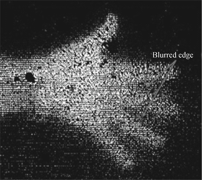
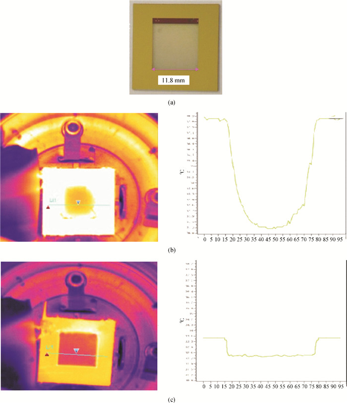
Infrared thermal imaging of the traditional substrate-free FPA
SEMICONDUCTOR DEVICES
Ruiwen Liu1, 2, Yanmei Kong1, 2, Binbin Jiao1, 2, , Zhigang Li1, 2, Haiping Shang1, 2, Dike Lu1, 2, Chaoqun Gao1, 2, Dapeng Chen1, 2 and Qingchuan Zhang2, 3
Corresponding author: Jiao Binbin, jiaobinb@ime.ac.cn
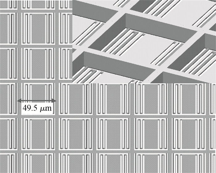
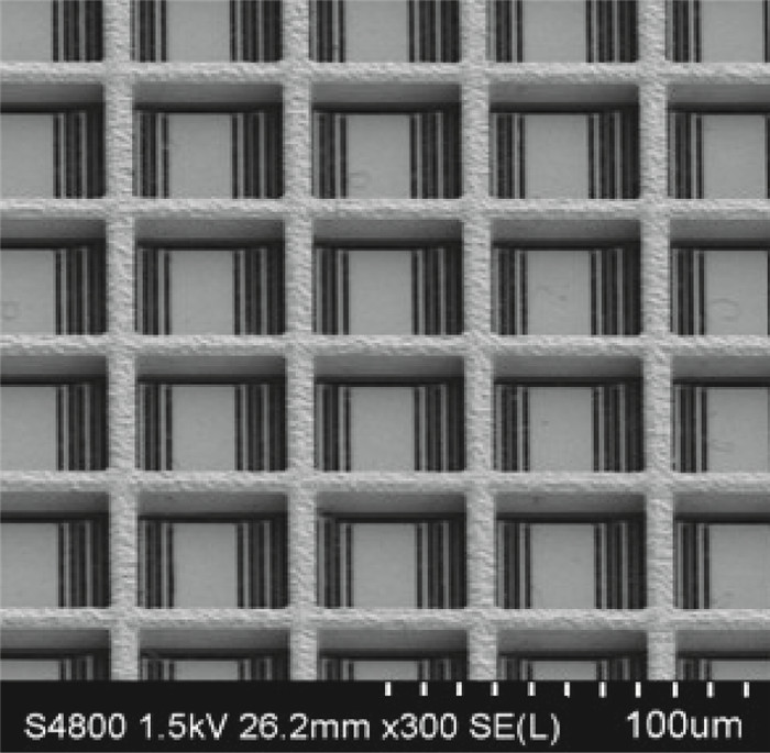
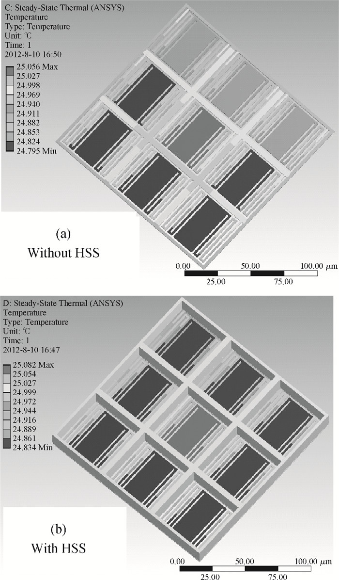
Abstract: A substrate-free optical readout focal plane array (FPA) operating in 8-12 μm with a heat sink structure (HSS) was fabricated and its performance was tested. The temperature distribution of the FPA with an HSS investigated by using a commercial FLIR IR camera shows excellent uniformity. The thermal cross-talk effect existing in traditional substrate-free FPAs was eliminated effectively. The heat sink is fabricated successfully by electroplating copper, which provides high thermal capacity and high thermal conductivity, on the frame of substrate-free FPA. The FPA was tested in the optical-readout system, the results show that the response and NETD are 13.6 grey/K (F/#=0.8) and 588 mK, respectively.
Keywords: infrared focal plane array, substrate-free, optical readout, heat sink structure
| [1] |
Grbovic D, Lavrik N V, Rajic S, et al. Arrays of SiO2 substrate-free micromechanical uncooled infrared and terahertz detectors. J Appl Phys, 2008, 104:054508 doi: 10.1063/1.2959574
|
| [2] |
Barnes J R, Stephenson R J, Woodburn C N, et al. A femtojoule calorimeter using micromechanical sensors. Rev Sci Instrum, 1994, 65:3793 doi: 10.1063/1.1144509
|
| [3] |
Duan Z H, Zhang Q C, Wu X P, et al. Uncooled optically readable bimaterial micro-cantilever infrared imaging device. Chin Phys Lett, 2003, 20(12):2130 doi: 10.1088/0256-307X/20/12/012
|
| [4] |
Dong F L, Zhang Q C, Chen D P, et al. Optimized optomechanical micro-cantilever array for uncooled infrared imaging. Chin Phys Lett, 2007, 24(12):3362 doi: 10.1088/0256-307X/24/12/020
|
| [5] |
Wang X, Ma S L, Yu X M, et al. IR imaging using a cantilever-based focal plane array fabricated by deep reactive ion etching technique. Appl Phys Lett, 2007, 91:054109 doi: 10.1063/1.2768024
|
| [6] |
Grbovic D, Lavrik N V, Datskos P G, et al. Uncooled infrared imaging using bimaterial microcantilever arrays. Appl Phys Lett, 2006, 89:073118 doi: 10.1063/1.2337083
|
| [7] |
Oden P I, Datskos P G, Thundat T, et al. Uncooled thermal imaging using a piezoresistive microcantilever. Appl Phys Lett, 1996, 69(21):3277 doi: 10.1063/1.117309
|
| [8] |
Varesi J, Lai J, Shi Z, et al. Photothermal measurements at picowatt resolution using uncooled micro-optomechanical sensors. Appl Phys Lett, 1997, 71(3):306 doi: 10.1063/1.120440
|
| [9] |
Zhao Y, Mao M Y, Horowitz R, et al. Optomechanical uncooled infrared imaging system:design, microfabrication, and performance. J Microelectromech Syst, 2002, 11(2):136 doi: 10.1109/84.993448
|
| [10] |
Perazzo T, Mao M, Kwon O, et al. Infrared vision using uncooled micro-optomechanical camera. Appl Phys Lett, 1999, 74(23):3567 doi: 10.1063/1.124163
|
| [11] |
Cheng T, Zhang Q C, Jiao B B, et al. Analysis of optical readout sensitivity for uncooled infrared detector. Chin Phys Lett, 2009, 26(12):124206 doi: 10.1088/0256-307X/26/12/124206
|
| [12] |
Li C B, Jiao B B, Shi S L, et al. A novel uncooled substrate-free optical-readable infrared detector:design, fabrication and performance. Meas Sci Technol, 2006, 17:1981 doi: 10.1088/0957-0233/17/7/042
|
| [13] |
Li Chaobo, Jiao Binbin, Shi Shali, et al. A MEMS based focus plane array for infrared imaging. Chinese Journal of Semiconductors, 2006, 27(1):150 doi: 10.1007/s11460-007-0015-x
|
| [14] |
Jiao B B, Li C B, Chen D P, et al. A novel opto-mechanical uncooled infrared detector. Infrared Phys Technol, 2007, 51:66 doi: 10.1016/j.infrared.2006.10.035
|
| [15] |
Xiong Z M, Zhang Q C, Gao J, et al. The pressure-dependent performance of a substrate-free focal plane array in an uncooled infrared imaging system. J Appl Phys, 2007, 102:113524 doi: 10.1063/1.2822333
|
| [16] |
Cheng T, Zhang Q C, Wu X P, et al. Uncooled infrared imaging using a substrate-free focal-plane array. IEEE Electron Device Lett, 2008, 29(11):1218 doi: 10.1109/LED.2008.2004568
|
| [17] |
Dong F, Zhang Q, Chen D, et al. An uncooled optically readable infrared imaging detector. Sens Actuators A, 2007, 133:236 doi: 10.1016/j.sna.2006.04.031
|
| [18] |
Jiang Xingkai, Zhang Qingchuan, Shi Haitao, et al. Analysis of theoretical model of thermal infrared imager based on the substrate-free focal plane array. Acta Phys Sin, 2011, 60(5):054401(in Chinese) http://wulixb.iphy.ac.cn/EN/abstract/abstract18388.shtml
|
| [19] |
Cheng T, Zhang Q C, Chen D P, et al. Performance of an optimized substrate-free focal plane array for optical readout uncooled infrared detector. J Appl Phys, 2009, 105:034505 doi: 10.1063/1.3073986
|
| [20] |
Chen Dapeng, Ye Tianchun, Xie Changqing, et al. Stress in SiNx film embedded with silicon nanocrystals preparing by LPCVD. Chinese Journal of Semiconductors, 2001, 22(12):1529(in Chinese)
|


Article views: 2467 Times PDF downloads: 11 Times Cited by: 0 Times
Received: 17 July 2012 Revised: 24 August 2012 Online: Published: 01 February 2013
| Citation: |
Ruiwen Liu, Yanmei Kong, Binbin Jiao, Zhigang Li, Haiping Shang, Dike Lu, Chaoqun Gao, Dapeng Chen, Qingchuan Zhang. A substrate-free optical readout focal plane array with a heat sink structure[J]. Journal of Semiconductors, 2013, 34(2): 024005. doi: 10.1088/1674-4926/34/2/024005
****
R W Liu, Y M Kong, B B Jiao, Z G Li, H P Shang, D K Lu, C Q Gao, D P Chen, Q C Zhang. A substrate-free optical readout focal plane array with a heat sink structure[J]. J. Semicond., 2013, 34(2): 024005. doi: 10.1088/1674-4926/34/2/024005.

|
| [1] |
Grbovic D, Lavrik N V, Rajic S, et al. Arrays of SiO2 substrate-free micromechanical uncooled infrared and terahertz detectors. J Appl Phys, 2008, 104:054508 doi: 10.1063/1.2959574
|
| [2] |
Barnes J R, Stephenson R J, Woodburn C N, et al. A femtojoule calorimeter using micromechanical sensors. Rev Sci Instrum, 1994, 65:3793 doi: 10.1063/1.1144509
|
| [3] |
Duan Z H, Zhang Q C, Wu X P, et al. Uncooled optically readable bimaterial micro-cantilever infrared imaging device. Chin Phys Lett, 2003, 20(12):2130 doi: 10.1088/0256-307X/20/12/012
|
| [4] |
Dong F L, Zhang Q C, Chen D P, et al. Optimized optomechanical micro-cantilever array for uncooled infrared imaging. Chin Phys Lett, 2007, 24(12):3362 doi: 10.1088/0256-307X/24/12/020
|
| [5] |
Wang X, Ma S L, Yu X M, et al. IR imaging using a cantilever-based focal plane array fabricated by deep reactive ion etching technique. Appl Phys Lett, 2007, 91:054109 doi: 10.1063/1.2768024
|
| [6] |
Grbovic D, Lavrik N V, Datskos P G, et al. Uncooled infrared imaging using bimaterial microcantilever arrays. Appl Phys Lett, 2006, 89:073118 doi: 10.1063/1.2337083
|
| [7] |
Oden P I, Datskos P G, Thundat T, et al. Uncooled thermal imaging using a piezoresistive microcantilever. Appl Phys Lett, 1996, 69(21):3277 doi: 10.1063/1.117309
|
| [8] |
Varesi J, Lai J, Shi Z, et al. Photothermal measurements at picowatt resolution using uncooled micro-optomechanical sensors. Appl Phys Lett, 1997, 71(3):306 doi: 10.1063/1.120440
|
| [9] |
Zhao Y, Mao M Y, Horowitz R, et al. Optomechanical uncooled infrared imaging system:design, microfabrication, and performance. J Microelectromech Syst, 2002, 11(2):136 doi: 10.1109/84.993448
|
| [10] |
Perazzo T, Mao M, Kwon O, et al. Infrared vision using uncooled micro-optomechanical camera. Appl Phys Lett, 1999, 74(23):3567 doi: 10.1063/1.124163
|
| [11] |
Cheng T, Zhang Q C, Jiao B B, et al. Analysis of optical readout sensitivity for uncooled infrared detector. Chin Phys Lett, 2009, 26(12):124206 doi: 10.1088/0256-307X/26/12/124206
|
| [12] |
Li C B, Jiao B B, Shi S L, et al. A novel uncooled substrate-free optical-readable infrared detector:design, fabrication and performance. Meas Sci Technol, 2006, 17:1981 doi: 10.1088/0957-0233/17/7/042
|
| [13] |
Li Chaobo, Jiao Binbin, Shi Shali, et al. A MEMS based focus plane array for infrared imaging. Chinese Journal of Semiconductors, 2006, 27(1):150 doi: 10.1007/s11460-007-0015-x
|
| [14] |
Jiao B B, Li C B, Chen D P, et al. A novel opto-mechanical uncooled infrared detector. Infrared Phys Technol, 2007, 51:66 doi: 10.1016/j.infrared.2006.10.035
|
| [15] |
Xiong Z M, Zhang Q C, Gao J, et al. The pressure-dependent performance of a substrate-free focal plane array in an uncooled infrared imaging system. J Appl Phys, 2007, 102:113524 doi: 10.1063/1.2822333
|
| [16] |
Cheng T, Zhang Q C, Wu X P, et al. Uncooled infrared imaging using a substrate-free focal-plane array. IEEE Electron Device Lett, 2008, 29(11):1218 doi: 10.1109/LED.2008.2004568
|
| [17] |
Dong F, Zhang Q, Chen D, et al. An uncooled optically readable infrared imaging detector. Sens Actuators A, 2007, 133:236 doi: 10.1016/j.sna.2006.04.031
|
| [18] |
Jiang Xingkai, Zhang Qingchuan, Shi Haitao, et al. Analysis of theoretical model of thermal infrared imager based on the substrate-free focal plane array. Acta Phys Sin, 2011, 60(5):054401(in Chinese) http://wulixb.iphy.ac.cn/EN/abstract/abstract18388.shtml
|
| [19] |
Cheng T, Zhang Q C, Chen D P, et al. Performance of an optimized substrate-free focal plane array for optical readout uncooled infrared detector. J Appl Phys, 2009, 105:034505 doi: 10.1063/1.3073986
|
| [20] |
Chen Dapeng, Ye Tianchun, Xie Changqing, et al. Stress in SiNx film embedded with silicon nanocrystals preparing by LPCVD. Chinese Journal of Semiconductors, 2001, 22(12):1529(in Chinese)
|

 WeChat ID
Journal of Semiconductors © 2017 All Rights Reserved 京ICP备05085259号-2

 DownLoad: