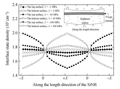
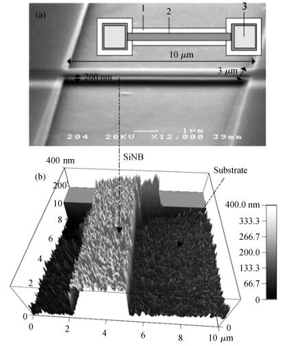
| [1] |
Cui Y, Zhong Z H, Wang D L, et al. High performance silicon nanowire field effect transistors. Nano Lett, 2003, 3(2):149 doi: 10.1021/nl025875l |
| [2] |
Li X X, Ono T, Wang Y L, et al. Ultrathin single-crystalline-silicon cantilever resonators:fabrication technology and significant specimen size effect on Young's modulus. Appl Phys Lett, 2003, 83(15):3081 doi: 10.1063/1.1618369 |
| [3] |
Li D, Wu Y, Kim P, et al. Thermal conductivity of individual silicon nanowires. Appl Phys Lett, 2003, 83(14):2934 doi: 10.1063/1.1616981 |
| [4] |
He R R, Yang P D. Giant piezoresistance effect in silicon nanowires. Nature Nanotechnology, 2006, 1:42 doi: 10.1038/nnano.2006.53 |
| [5] |
Yang Y L, Li X X. Giant piezoresistance of p-type nano-thick silicon induced by interface electron trapping instead of 2D quantum confinement. Nanotechnology, 2011, 22(1):015501 doi: 10.1088/0957-4484/22/1/015501 |
| [6] |
|
| [7] |
Chuai Rongyan, Liu Bin, Liu Xiaowei, et al. Tunnelling piezoresistive effect of grain boundary in polysilicon nano-films. Journal of Semiconductors, 2010, 31(3):032002 doi: 10.1088/1674-4926/31/3/032002 |
| [8] |
Brönstrup G, Jahr N, Leiterer C, et al. Optical properties of individual silicon nanowires for photonic devices. ACS Nano, 2010, 4(12):7113 doi: 10.1021/nn101076t |
| [9] |
Fernandez-Sierra M V, Adessi C, Blase X. Conductance, surface traps, and passivation in doped silicon nanowires. Nano Lett, 2006, 6(12):2674 doi: 10.1021/nl0614258 |
| [10] |
Vo T, Williamson A J, Galli G. First principles simulations of the structural and electronic properties of silicon nanowires. Phys Rev B, 2006, 74:045116 doi: 10.1103/PhysRevB.74.045116 |
| [11] |
Vaurette F, Nys J P, Deresmes D, et al. Resistivity and surface states density of n-and p-type silicon nanowires. J Vac Sci Technol B, 2008, 26(3):945 doi: 10.1116/1.2908438 |
| [12] |
Kimukin I, Islam M S, Williams R S. Surface depletion thickness of p-doped silicon nanowires grown using metal-catalysed chemical vapour deposition. Nanotechnology, 2006, 17:S240
|
| [13] |
Park J T, Kim J Y, Islam M S. Extraction of doping concentration and interface state density in silicon nanowires. IEEE Trans Nanotechnol, 2011, 10(5):1004 doi: 10.1109/TNANO.2010.2094203 |
| [14] |
Schmidt V, Senz S, Gösele U. Influence of the Si/SiO2 interface on the charge carrier density of Si nanowires. Appl Phys A, 2007, 86(2):187
|
| [15] |
Sato S, Li W, Kakushima K, et al. Extraction of additional interfacial states of silicon nanowire field-effect transistors. Appl Phys Lett, 2011, 98(23):233506 doi: 10.1063/1.3598402 |
| [16] |
Zhang J H, Mao X L, Liu Q Q, et al. Mechanical properties of silicon nanobeams with undercut evaluated by combining dynamic resonance test and finite element analysis. Chin Phys B, 2012, 21(8):086101 doi: 10.1088/1674-1056/21/8/086101 |
| [17] |
Diarra M, Niquet Y M, Delerue C, et al. Ionization energy of donor and acceptor impurities in semiconductor nanowires:importance of dielectric confinement. Phys Rev B, 2007, 75:045301 doi: 10.1103/PhysRevB.75.045301 |
| [18] |
Sadeghian H, Yang C K, Goosen J F L, et al. Effects of size and defects on the elasticity of silicon nanocantilevers. J Micromech Microeng, 2010, 20:064012 doi: 10.1088/0960-1317/20/6/064012 |
| [19] |
Zhang Xingli, Sun Zhaowei. Effects of vacancy structural defects on the thermal conductivity of silicon thin films. Journal of Semiconductors, 2011, 32(5):053002 doi: 10.1088/1674-4926/32/5/053002 |
| [20] |
Zhu Huiwen, Liu Yongsong, Mao Lingfeng, et al. Theoretical study of the SiO 2/Si interface and its effect on energy band profile and MOSFET gate tunneling current. Journal of Semiconductors, 2010, 31(8):082003 doi: 10.1088/1674-4926/31/8/082003 |
| [21] |
Sze S M. Physics of semiconductor devices. New York: John Wiley & Sons, 1981
|
| [22] |
Li G, Aluru N R. A Lagrangian approach for quantum-mechanical electrostatic analysis of deformable silicon nanostructures. Engineering Analysis with Boundary Elements, 2006, 30(11):925 doi: 10.1016/j.enganabound.2006.03.012 |
| [23] |
Nghiêm T T T, Aubry-Fortuna V, Chassat C, et al. Monte Carlo simulation of giant piezoresistance effect in p-type silicon nanostructures. Mod Phys Lett B, 2011, 25(12/13):995
|
| [24] |
|
| [25] |
Angermann H, Henrion W, Röseler A, et al. Wet-chemical passivation of Si (111)-and Si (100)-substrates. Mater Sci Eng B, 2000, 73(1):178
|


 DownLoad: