


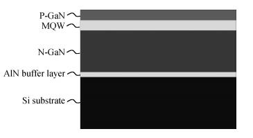
Fig. 1.
Schematic cross-sectional drawing of GaN-based MQW EPI layers grown on Si substrate.
SEMICONDUCTOR MATERIALS
Shaohua Zhang1, 2, , Bo Feng1, 2, Qian Sun2 and Hanmin Zhao2
Corresponding author: Zhang Shaohua, Email:zhangshaohua2013@163.com
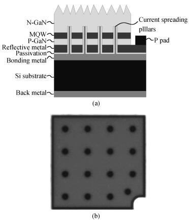
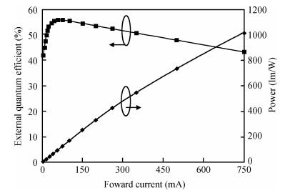
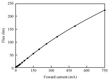
Abstract: GaN based MQW epitaxial layers were grown on Si (111) substrate by MOCVD using AlN as the buffer layer. High light extraction LEDs were prepared by substrate transferring technology in combination with thin-film and flip-chip design. The blue and white 1.1×1.1 mm2 LED lamps are measured. The optical powers and external quantum efficiency for silicone encapsulated blue lamp are 546 mW, and 50.3% at forward current of 350 mA, while the photometric light output for a white lamp packaged with standard YAG phosphor is 120.1 lm.
Keywords: silicon substrate, GaN, flip chip, LED
| [1] | |
| [2] |
Chu C F, Yu C C, Cheng H C, et al. Comparison of p-side down and p-side up GaN light-emitting diodes fabricated by laser lift-off. Jpn J Appl Phys, 2003, 42:L147 doi: 10.1143/JJAP.42.L147
|
| [3] |
Fujii T, Gao Y, Sharma R, et al. Increase in the extraction effi-ciency of GaN-based light-emitting diodes via surface roughen-ing. Appl Phys Lett, 2004, 84:855 doi: 10.1063/1.1645992
|
| [4] |
Tu S H, Chen J C, Hwu F S, et al. Characteristics of current distribution by designed electrode patterns for high power thin GaN LED. Solid-State Electron, 2010, 54:1438 doi: 10.1016/j.sse.2010.04.044
|
| [5] |
Shchekin O B, Epler J E, Trottier T A, et al. High performance thin-film flip-chip InGaN-GaN light-emitting diode. Appl Phys Lett, 2006, 89:071109 doi: 10.1063/1.2337007
|
| [6] |
Minsky M S, White M, Hu E L. Room-temperature photoenhanced wet etching of GaN. Appl Phys Lett, 1996, 68:1531 doi: 10.1063/1.115689
|


Article views: 3926 Times PDF downloads: 36 Times Cited by: 0 Times
Received: 27 November 2012 Revised: 04 December 2012 Online: Published: 01 May 2013
| Citation: |
Shaohua Zhang, Bo Feng, Qian Sun, Hanmin Zhao. Preparation of GaN-on-Si based thin-film flip-chip LEDs[J]. Journal of Semiconductors, 2013, 34(5): 053006. doi: 10.1088/1674-4926/34/5/053006
****
S H Zhang, B Feng, Q Sun, H M Zhao. Preparation of GaN-on-Si based thin-film flip-chip LEDs[J]. J. Semicond., 2013, 34(5): 053006. doi: 10.1088/1674-4926/34/5/053006.

|
| [1] | |
| [2] |
Chu C F, Yu C C, Cheng H C, et al. Comparison of p-side down and p-side up GaN light-emitting diodes fabricated by laser lift-off. Jpn J Appl Phys, 2003, 42:L147 doi: 10.1143/JJAP.42.L147
|
| [3] |
Fujii T, Gao Y, Sharma R, et al. Increase in the extraction effi-ciency of GaN-based light-emitting diodes via surface roughen-ing. Appl Phys Lett, 2004, 84:855 doi: 10.1063/1.1645992
|
| [4] |
Tu S H, Chen J C, Hwu F S, et al. Characteristics of current distribution by designed electrode patterns for high power thin GaN LED. Solid-State Electron, 2010, 54:1438 doi: 10.1016/j.sse.2010.04.044
|
| [5] |
Shchekin O B, Epler J E, Trottier T A, et al. High performance thin-film flip-chip InGaN-GaN light-emitting diode. Appl Phys Lett, 2006, 89:071109 doi: 10.1063/1.2337007
|
| [6] |
Minsky M S, White M, Hu E L. Room-temperature photoenhanced wet etching of GaN. Appl Phys Lett, 1996, 68:1531 doi: 10.1063/1.115689
|

 WeChat ID
Journal of Semiconductors © 2017 All Rights Reserved 京ICP备05085259号-2

 DownLoad:

