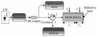
Fig. 1.
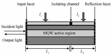
Schematic diagram of the two-section MQW-RSOA.
SEMICONDUCTOR DEVICES
Huali Xi, Lirong Huang and Guiying Jiang
Corresponding author: Huang Lirong, Email:hlr5649@163.com
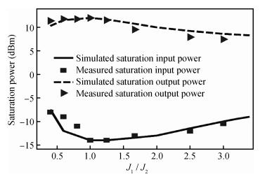
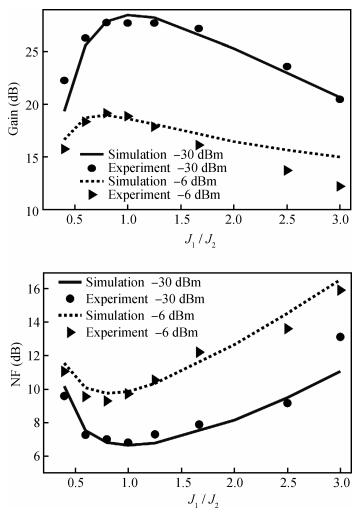
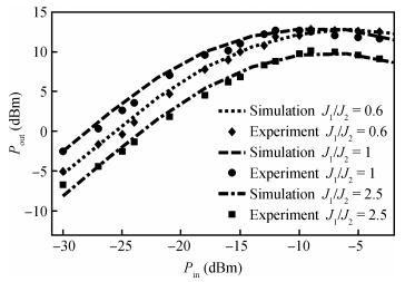
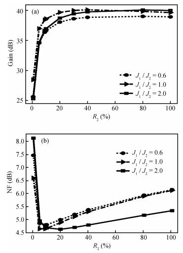
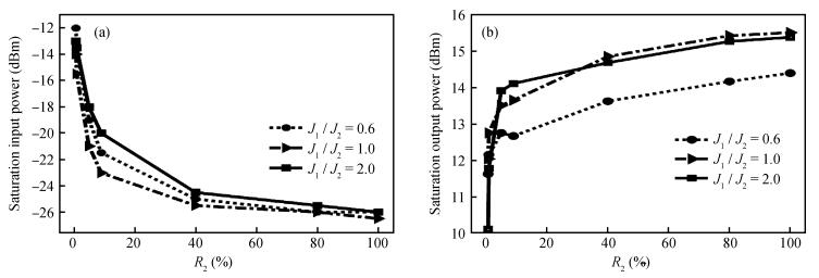
Abstract: A 1.3 μ m two-section multi-quantum well reflective semiconductor optical amplifier is designed and fabricated. The impacts of injection current density ratio and the reflectivity of the reflective facet on gain, saturation and noise characteristics are studied theoretically and experimentally. The results indicate that the gain and saturation power can be easily manipulated by changing the current density ratio; and better gain and noise characteristics can be obtained when the reflectivity is appropriately selected.
Keywords: reflective semiconductor optical amplifier, two-section RSOA, gain, noise figure, current density ratio
| [1] |
Lee W, Park M Y, Cho S H, et al. Bidirectional WDM-PON based on gain-saturated reflective semiconductor optical amplifiers. IEEE Photonics Technol Lett, 2005, 17:2460 doi: 10.1109/LPT.2005.858148
|
| [2] |
Kim B W. RSOA-based wavelength-reuse gigabit WDM-PON. Journal of the Optical Society of Korea, 2008, 12:337 doi: 10.3807/JOSK.2008.12.4.337
|
| [3] |
Won Y Y, Kwon H C, Han S K, et al. OBI noise reduction using gain saturated SOA in reflective SOA based WDM/SCM-PON optical links. Electron Lett, 2006, 42:992 doi: 10.1049/el:20061202
|
| [4] |
Yu Y, Huang L R, Xiong M, et al. Enhancement of gain recovery rate and cross-gain modulation bandwidth using a two-electrode quantum-dot semiconductor optical amplifier. J Opt Soc America B, 2010, 27:2211 doi: 10.1364/JOSAB.27.002211
|
| [5] |
Tian P, Huang L R, Hong W, et al. Pattern effect reduction in all optical wavelength conversion using a two-electrode semiconductor optical amplifier. Appl Opt, 2010, 49:5005 doi: 10.1364/AO.49.005005
|
| [6] |
Wang Hanchao, Huang Lirong, Shi Zhongwei. Amplified spontaneous emission spectrum and gain characteristic of a two-electrode semiconductor optical amplifier. Journal of Semiconductors, 2011, 32:064010 doi: 10.1088/1674-4926/32/6/064010
|
| [7] |
Djordjev K, Choi S J, Choi W J, et al. Two-segment spectrally inhomogeneous traveling wave semiconductor optical amplifiers applied to spectral equalization. IEEE Photonics Technol Lett, 2002, 14:603 doi: 10.1109/68.998698
|
| [8] |
Kim H S, Choi B S, Kim K S, et al. Improvement of modulation bandwidth in multi-section RSOA for colorless WDM-PON. Opt Express, 2009, 17:16732
|
| [9] |
De Valicourt G, Lamponi M, Duan G H, et al. Chirp reduction in directly modulated multi-electrode RSOA devices in passive optical networks. IEEE Photonics Technol Lett, 2010, 22:1425 doi: 10.1109/LPT.2010.2062496
|
| [10] |
De Valicourt G, Lamponi M, Duan G H, et al. First 100 km uplink transmission at 2. 5 Gbit/s for hybrid WDM/TDM PON based on optimized bi-electrode RSOA. European Conference and Exhibition on Optical Communication (ECOC), 2010: Tu. 5. B. 6
|
| [11] |
Nielsen M L, Mork J, Suzuki R, et al. Experimental and theoretical investigation of the impact of ultra-fast carrier dynamics on high-speed SOA-based all-optical switches. Opt Express, 2006, 14:331 doi: 10.1364/OPEX.14.000331
|
| [12] |
Nguyen L V T, Lowery A J, Gurney P C R, et al. A time-domain model for high-speed quantum well lasers including carrier transport effects. IEEE J Sel Topics Quantum Electron, 1995, 1:494 doi: 10.1109/2944.401234
|
| [13] |
Lennox R, Carney K, Maldonado-Basilio R, et al. Impact of bias current distribution on the noise figure and power saturation of a multi-contact semiconductor optical amplifier. Opt Lett, 2011, 36:2521 doi: 10.1364/OL.36.002521
|
| [14] |
Baney D M, Gallion P, Tucker R S. Theory and measurement techniques for the noise figure of optical amplifiers. Opt Fiber Technol, 2000, 6:122 doi: 10.1006/ofte.2000.0327
|
| [15] |
Donati S, Giuliani G. Noise in an optical amplifier:formulation of a new semiclassical model. IEEE J Quantum Electron, 1997, 33:1481 doi: 10.1109/3.622626
|


Article views: 2437 Times PDF downloads: 11 Times Cited by: 0 Times
Received: 13 September 2012 Revised: 12 November 2012 Online: Published: 01 May 2013
| Citation: |
Huali Xi, Lirong Huang, Guiying Jiang. The effects of current density ratio and reflectivity on the gain, saturation and noise characteristics of a two-section MQW RSOA[J]. Journal of Semiconductors, 2013, 34(5): 054004. doi: 10.1088/1674-4926/34/5/054004
****
H L Xi, L R Huang, G Y Jiang. The effects of current density ratio and reflectivity on the gain, saturation and noise characteristics of a two-section MQW RSOA[J]. J. Semicond., 2013, 34(5): 054004. doi: 10.1088/1674-4926/34/5/054004.

|
| [1] |
Lee W, Park M Y, Cho S H, et al. Bidirectional WDM-PON based on gain-saturated reflective semiconductor optical amplifiers. IEEE Photonics Technol Lett, 2005, 17:2460 doi: 10.1109/LPT.2005.858148
|
| [2] |
Kim B W. RSOA-based wavelength-reuse gigabit WDM-PON. Journal of the Optical Society of Korea, 2008, 12:337 doi: 10.3807/JOSK.2008.12.4.337
|
| [3] |
Won Y Y, Kwon H C, Han S K, et al. OBI noise reduction using gain saturated SOA in reflective SOA based WDM/SCM-PON optical links. Electron Lett, 2006, 42:992 doi: 10.1049/el:20061202
|
| [4] |
Yu Y, Huang L R, Xiong M, et al. Enhancement of gain recovery rate and cross-gain modulation bandwidth using a two-electrode quantum-dot semiconductor optical amplifier. J Opt Soc America B, 2010, 27:2211 doi: 10.1364/JOSAB.27.002211
|
| [5] |
Tian P, Huang L R, Hong W, et al. Pattern effect reduction in all optical wavelength conversion using a two-electrode semiconductor optical amplifier. Appl Opt, 2010, 49:5005 doi: 10.1364/AO.49.005005
|
| [6] |
Wang Hanchao, Huang Lirong, Shi Zhongwei. Amplified spontaneous emission spectrum and gain characteristic of a two-electrode semiconductor optical amplifier. Journal of Semiconductors, 2011, 32:064010 doi: 10.1088/1674-4926/32/6/064010
|
| [7] |
Djordjev K, Choi S J, Choi W J, et al. Two-segment spectrally inhomogeneous traveling wave semiconductor optical amplifiers applied to spectral equalization. IEEE Photonics Technol Lett, 2002, 14:603 doi: 10.1109/68.998698
|
| [8] |
Kim H S, Choi B S, Kim K S, et al. Improvement of modulation bandwidth in multi-section RSOA for colorless WDM-PON. Opt Express, 2009, 17:16732
|
| [9] |
De Valicourt G, Lamponi M, Duan G H, et al. Chirp reduction in directly modulated multi-electrode RSOA devices in passive optical networks. IEEE Photonics Technol Lett, 2010, 22:1425 doi: 10.1109/LPT.2010.2062496
|
| [10] |
De Valicourt G, Lamponi M, Duan G H, et al. First 100 km uplink transmission at 2. 5 Gbit/s for hybrid WDM/TDM PON based on optimized bi-electrode RSOA. European Conference and Exhibition on Optical Communication (ECOC), 2010: Tu. 5. B. 6
|
| [11] |
Nielsen M L, Mork J, Suzuki R, et al. Experimental and theoretical investigation of the impact of ultra-fast carrier dynamics on high-speed SOA-based all-optical switches. Opt Express, 2006, 14:331 doi: 10.1364/OPEX.14.000331
|
| [12] |
Nguyen L V T, Lowery A J, Gurney P C R, et al. A time-domain model for high-speed quantum well lasers including carrier transport effects. IEEE J Sel Topics Quantum Electron, 1995, 1:494 doi: 10.1109/2944.401234
|
| [13] |
Lennox R, Carney K, Maldonado-Basilio R, et al. Impact of bias current distribution on the noise figure and power saturation of a multi-contact semiconductor optical amplifier. Opt Lett, 2011, 36:2521 doi: 10.1364/OL.36.002521
|
| [14] |
Baney D M, Gallion P, Tucker R S. Theory and measurement techniques for the noise figure of optical amplifiers. Opt Fiber Technol, 2000, 6:122 doi: 10.1006/ofte.2000.0327
|
| [15] |
Donati S, Giuliani G. Noise in an optical amplifier:formulation of a new semiclassical model. IEEE J Quantum Electron, 1997, 33:1481 doi: 10.1109/3.622626
|

 WeChat ID
Journal of Semiconductors © 2017 All Rights Reserved 京ICP备05085259号-2

 DownLoad: