


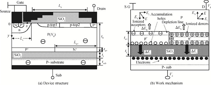
Fig. 1.
Structure and mechanism of the FBL SOI pLDMOS.
SEMICONDUCTOR DEVICES
Lijuan Wu1, 2, , Wentong Zhang2, Bo Zhang2 and Zhaoji Li2
Corresponding author: Wu Lijuan, Email:ljwu@cuit.edu.cn
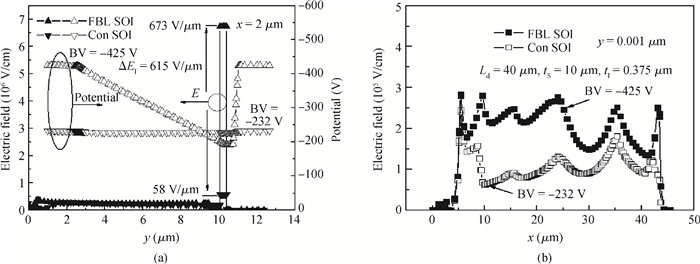
Abstract: A novel silicon-on-insulator (SOI) high-voltage pLDMOS is presented with a partial interface equipotential floating buried layer (FBL) and its analytical model is analyzed in this paper. The surface heavily doped p-top layers, interface floating buried N+/P+ layers, and three-step field plates are designed carefully in the FBL SOI pLDMOS to optimize the electric field distribution of the drift region and reduce the specific resistance. On the condition of ESIMOX (epoxy separated by implanted oxygen), it has been shown that the breakdown voltage of the FBL SOI pLDMOS is increased from-232 V of the conventional SOI to-425 V and the specific resistance Ron, sp is reduced from 0.88 to 0.2424 Ω·cm2.
| [1] |
Sunkavalli R, Tamba A, Bbaliga B J. Step drift doping profile for high voltage DI lateral power devices. IEEE International SOI Conference, 1995:139 http://ieeexplore.ieee.org/document/526499/?arnumber=526499
|
| [2] |
Zhang S D, Sin J K O, Lai T M L, et al. Numerical model of linear doping profiles for high-voltage thin-film SOI devices. IEEE Trans Electron Devices, 1999, 46(5):1036 doi: 10.1109/16.760414
|
| [3] |
Zhu Mingda, Wang Juncheng, Du Gang. Design and optimization of a novel SOl LDMOS structure using PIN junction. IEEE International Conference of Electron Devices and Solid-State Circuits (EDSSC), 2010:1 http://www.sciencedirect.com/science/article/pii/S1350449515000766
|
| [4] |
Zingg R P, Weijland I, Zwol H V, et al. 850 V DMOS-switch in silicon-on insulator with specific Ron 13Ω·mm2. IEEE International SOI Conference, 2000:62
|
| [5] |
Xu S, Gan K P, Samudra G S, et al. 120 V interdigitated-drain LDMOS (IDLDMOS) on SOI substrated breaking power LDMOS limit. IEEE Trans Electron Devices, 2000, 47(10):1980 doi: 10.1109/16.870584
|
| [6] |
Chung S K. An analytical model for breakdown voltage of surface implanted SOI RESURF LDMOS. IEEE Trans Electron Devices, 2000, 47(5):1006 doi: 10.1109/16.841233
|
| [7] |
Kim H W, Choi Y I, Chung S K. Linearly-graded surface-doped SOI LDMOSFET with recessed source. Microelectron Eng, 2000, 51:547 http://www.sciencedirect.com/science/article/pii/S0167931799005171
|
| [8] |
Yoo S J, Kim S H, Choi Y I, et al. Numerical analysis of SOI LDMOS using a recessed source and a trench drain. Microelectron J, 2000, 31:963 doi: 10.1016/S0026-2692(00)00094-X
|
| [9] |
Duan B, Zhang B, Li Z. New thin-film power MOSFETS with a buried oxide double step structure. IEEE Electron Device Lett, 2006, 27(5):377 doi: 10.1109/LED.2006.872904
|
| [10] |
Luo X, Zhang B, Li Z, et al. A novel 700-V SOI LDMOS with double-side trench. IEEE Electron Device Lett, 2007, 28(5):422 doi: 10.1109/LED.2007.894648
|


Article views: 2889 Times PDF downloads: 32 Times Cited by: 0 Times
Received: 06 December 2012 Revised: 25 January 2013 Online: Published: 01 July 2013
| Citation: |
Lijuan Wu, Wentong Zhang, Bo Zhang, Zhaoji Li. A high voltage SOI pLDMOS with a partial interface equipotential floating buried layer[J]. Journal of Semiconductors, 2013, 34(7): 074009. doi: 10.1088/1674-4926/34/7/074009
****
L J Wu, W T Zhang, B Zhang, Z J Li. A high voltage SOI pLDMOS with a partial interface equipotential floating buried layer[J]. J. Semicond., 2013, 34(7): 074009. doi: 10.1088/1674-4926/34/7/074009.

|
| [1] |
Sunkavalli R, Tamba A, Bbaliga B J. Step drift doping profile for high voltage DI lateral power devices. IEEE International SOI Conference, 1995:139 http://ieeexplore.ieee.org/document/526499/?arnumber=526499
|
| [2] |
Zhang S D, Sin J K O, Lai T M L, et al. Numerical model of linear doping profiles for high-voltage thin-film SOI devices. IEEE Trans Electron Devices, 1999, 46(5):1036 doi: 10.1109/16.760414
|
| [3] |
Zhu Mingda, Wang Juncheng, Du Gang. Design and optimization of a novel SOl LDMOS structure using PIN junction. IEEE International Conference of Electron Devices and Solid-State Circuits (EDSSC), 2010:1 http://www.sciencedirect.com/science/article/pii/S1350449515000766
|
| [4] |
Zingg R P, Weijland I, Zwol H V, et al. 850 V DMOS-switch in silicon-on insulator with specific Ron 13Ω·mm2. IEEE International SOI Conference, 2000:62
|
| [5] |
Xu S, Gan K P, Samudra G S, et al. 120 V interdigitated-drain LDMOS (IDLDMOS) on SOI substrated breaking power LDMOS limit. IEEE Trans Electron Devices, 2000, 47(10):1980 doi: 10.1109/16.870584
|
| [6] |
Chung S K. An analytical model for breakdown voltage of surface implanted SOI RESURF LDMOS. IEEE Trans Electron Devices, 2000, 47(5):1006 doi: 10.1109/16.841233
|
| [7] |
Kim H W, Choi Y I, Chung S K. Linearly-graded surface-doped SOI LDMOSFET with recessed source. Microelectron Eng, 2000, 51:547 http://www.sciencedirect.com/science/article/pii/S0167931799005171
|
| [8] |
Yoo S J, Kim S H, Choi Y I, et al. Numerical analysis of SOI LDMOS using a recessed source and a trench drain. Microelectron J, 2000, 31:963 doi: 10.1016/S0026-2692(00)00094-X
|
| [9] |
Duan B, Zhang B, Li Z. New thin-film power MOSFETS with a buried oxide double step structure. IEEE Electron Device Lett, 2006, 27(5):377 doi: 10.1109/LED.2006.872904
|
| [10] |
Luo X, Zhang B, Li Z, et al. A novel 700-V SOI LDMOS with double-side trench. IEEE Electron Device Lett, 2007, 28(5):422 doi: 10.1109/LED.2007.894648
|

 WeChat ID
Journal of Semiconductors © 2017 All Rights Reserved 京ICP备05085259号-2

 DownLoad:

