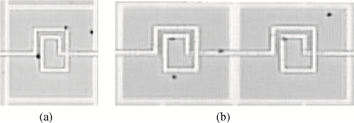
Fig. 1.
Microphotographs of the element inductor and the cascaded inductor. (a) Element inductor. (b) Cascaded inductor.
SEMICONDUCTOR INTEGRATED CIRCUITS
Corresponding author: Ye Yu, Email:yye@mail.sim.ac.cn
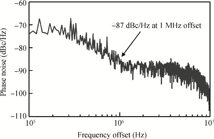
Abstract: A 50 GHz cross-coupled voltage controlled oscillator (VCO) considering the coupling effect of inductors based on a 65 nm standard complementary metal oxide semiconductor (CMOS) technology is reported. A pair of inductors has been fabricated, measured and analyzed to characterize the coupling effects of adjacent inductors. The results are then implemented to accurately evaluate the VCO's LC tank. By optimizing the tank voltage swing and the buffer's operation region, the VCO achieves a maximum efficiency of 11.4% by generating an average output power of 2.5 dBm while only consuming 19.7 mW (including buffers). The VCO exhibits a phase noise of-87 dBc/Hz at 1 MHz offset, leading to a figure of merit (FoM) of-167.5 dB/Hz and a tuning range of 3.8% (from 48.98 to 50.88 GHz).
Keywords: CMOS, coupling effects, inductors, LC tank, VCO
| [1] |
Hsieh H H, Lu L H. A V-band CMOS VCO with an admittance-transforming cross-coupled pair. IEEE J Solid-State Circuits, 2009, 44(6):1689 doi: 10.1109/JSSC.2009.2020203
|
| [2] |
Cao C, Kenneth K O. Millimeter-wave voltage-controlled oscillators in 0.13μm CMOS technology. IEEE J Solid-State Circuits, 2006, 41(6):1297 doi: 10.1109/JSSC.2006.874321
|
| [3] |
Huang G C, Kim S K, Gao Z Q, et al. A 45 GHz CMOS VCO adopting digitally switchable metal-oxide-metal capacitors. IEEE Microw Wireless Compon Lett, 2011, 21(5):270 doi: 10.1109/LMWC.2011.2124449
|
| [4] |
Kang K, Tan C J, Brinkhoff J, et al. Coupling effects between on-chip inductors in the millimeter-wave regime. IEEE Electron Device Lett, 2010, 31(4):362 doi: 10.1109/LED.2010.2041426
|
| [5] |
Yin W Y, Pan S J, Li L W, et al. Experimental characterization of coupling effects between two on-chip neighboring square inductors. IEEE Trans Electromagnetic Compatibility, 2003, 45(3):557 doi: 10.1109/TEMC.2003.815597
|
| [6] |
Gonzalez J L, Badets F, Martineau B, et al. A 56 GHz LC-tank VCO with 17% tuning range in 65 nm bulk CMOS for wireless HDMI. IEEE Trans Microw Theory Tech, 2010, 58(5):1359 doi: 10.1109/TMTT.2010.2042853
|
| [7] |
Kim N, Oh Y, Rieh J S. A 47 GHz LC cross-coupled VCO employing high-Q island-gate varactor for phase noise reduction. IEEE Microw Wireless Compon Lett, 2010, 20(2):94 doi: 10.1109/LMWC.2009.2038522
|
| [8] |
Kraemer M, Dragomirescu D, Plana R. A high efficiency differential 60 GHz VCO in a 65 nm CMOS technology for WSN applications. IEEE Microw Wireless Compon Lett, 2011, 21(6):314 doi: 10.1109/LMWC.2011.2134841
|
| [9] |
Hajimiri A, Lee T H. Design issues in CMOS differential LC oscillators. IEEE J Solid-State Circuits, 1999, 34(5):717 doi: 10.1109/4.760384
|
| [10] |
Chiu H C, Kao C P. A wide tuning range 69 GHz push-push VCO using 0.18μm CMOS technology. IEEE Microw Wireless Compon Lett, 2010, 20(2):97 doi: 10.1109/LMWC.2009.2038523
|
| [11] |
Li L, Reynaert P, Steyaert M. Design and analysis of a 90 nm mm-wave oscillator using inductive-division LC tank. IEEE J Solid-State Circuits, 2009, 44(7):1950 doi: 10.1109/JSSC.2009.2020245
|
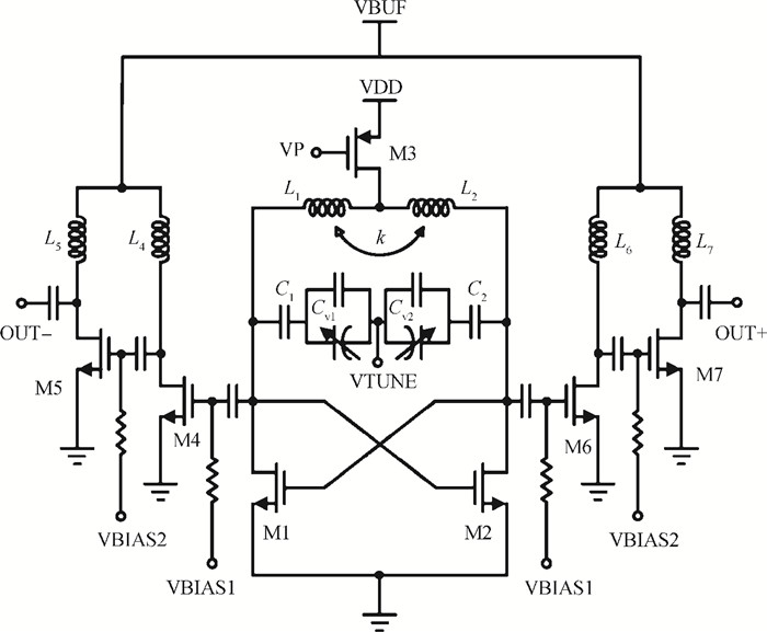
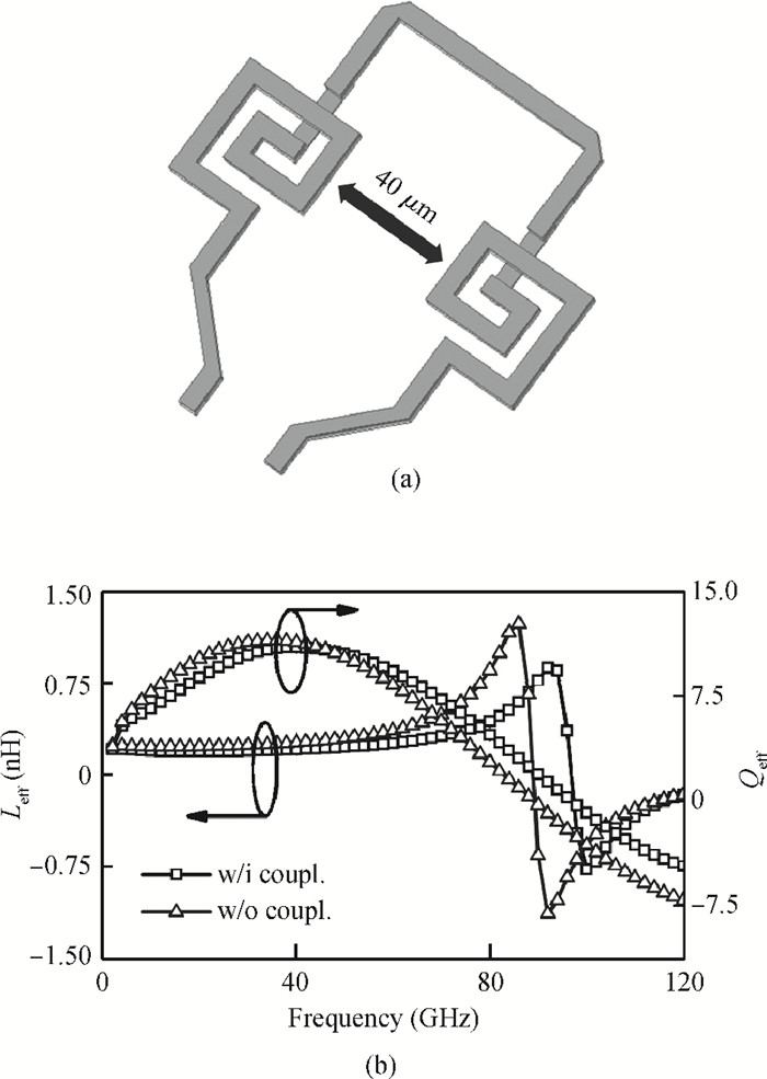
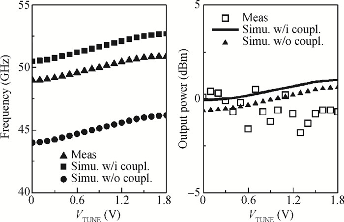
Table 1. Compared performance of VCOS.

|
| [1] |
Hsieh H H, Lu L H. A V-band CMOS VCO with an admittance-transforming cross-coupled pair. IEEE J Solid-State Circuits, 2009, 44(6):1689 doi: 10.1109/JSSC.2009.2020203
|
| [2] |
Cao C, Kenneth K O. Millimeter-wave voltage-controlled oscillators in 0.13μm CMOS technology. IEEE J Solid-State Circuits, 2006, 41(6):1297 doi: 10.1109/JSSC.2006.874321
|
| [3] |
Huang G C, Kim S K, Gao Z Q, et al. A 45 GHz CMOS VCO adopting digitally switchable metal-oxide-metal capacitors. IEEE Microw Wireless Compon Lett, 2011, 21(5):270 doi: 10.1109/LMWC.2011.2124449
|
| [4] |
Kang K, Tan C J, Brinkhoff J, et al. Coupling effects between on-chip inductors in the millimeter-wave regime. IEEE Electron Device Lett, 2010, 31(4):362 doi: 10.1109/LED.2010.2041426
|
| [5] |
Yin W Y, Pan S J, Li L W, et al. Experimental characterization of coupling effects between two on-chip neighboring square inductors. IEEE Trans Electromagnetic Compatibility, 2003, 45(3):557 doi: 10.1109/TEMC.2003.815597
|
| [6] |
Gonzalez J L, Badets F, Martineau B, et al. A 56 GHz LC-tank VCO with 17% tuning range in 65 nm bulk CMOS for wireless HDMI. IEEE Trans Microw Theory Tech, 2010, 58(5):1359 doi: 10.1109/TMTT.2010.2042853
|
| [7] |
Kim N, Oh Y, Rieh J S. A 47 GHz LC cross-coupled VCO employing high-Q island-gate varactor for phase noise reduction. IEEE Microw Wireless Compon Lett, 2010, 20(2):94 doi: 10.1109/LMWC.2009.2038522
|
| [8] |
Kraemer M, Dragomirescu D, Plana R. A high efficiency differential 60 GHz VCO in a 65 nm CMOS technology for WSN applications. IEEE Microw Wireless Compon Lett, 2011, 21(6):314 doi: 10.1109/LMWC.2011.2134841
|
| [9] |
Hajimiri A, Lee T H. Design issues in CMOS differential LC oscillators. IEEE J Solid-State Circuits, 1999, 34(5):717 doi: 10.1109/4.760384
|
| [10] |
Chiu H C, Kao C P. A wide tuning range 69 GHz push-push VCO using 0.18μm CMOS technology. IEEE Microw Wireless Compon Lett, 2010, 20(2):97 doi: 10.1109/LMWC.2009.2038523
|
| [11] |
Li L, Reynaert P, Steyaert M. Design and analysis of a 90 nm mm-wave oscillator using inductive-division LC tank. IEEE J Solid-State Circuits, 2009, 44(7):1950 doi: 10.1109/JSSC.2009.2020245
|


Article views: 2298 Times PDF downloads: 15 Times Cited by: 0 Times
Received: 26 November 2012 Revised: 27 January 2013 Online: Published: 01 July 2013
| Citation: |
Yu Ye, Tong Tian. A 65 nm CMOS high efficiency 50 GHz VCO with regard to the coupling effect of inductors[J]. Journal of Semiconductors, 2013, 34(7): 075001. doi: 10.1088/1674-4926/34/7/075001
****
Y Ye, T Tian. A 65 nm CMOS high efficiency 50 GHz VCO with regard to the coupling effect of inductors[J]. J. Semicond., 2013, 34(7): 075001. doi: 10.1088/1674-4926/34/7/075001.

|
| [1] |
Hsieh H H, Lu L H. A V-band CMOS VCO with an admittance-transforming cross-coupled pair. IEEE J Solid-State Circuits, 2009, 44(6):1689 doi: 10.1109/JSSC.2009.2020203
|
| [2] |
Cao C, Kenneth K O. Millimeter-wave voltage-controlled oscillators in 0.13μm CMOS technology. IEEE J Solid-State Circuits, 2006, 41(6):1297 doi: 10.1109/JSSC.2006.874321
|
| [3] |
Huang G C, Kim S K, Gao Z Q, et al. A 45 GHz CMOS VCO adopting digitally switchable metal-oxide-metal capacitors. IEEE Microw Wireless Compon Lett, 2011, 21(5):270 doi: 10.1109/LMWC.2011.2124449
|
| [4] |
Kang K, Tan C J, Brinkhoff J, et al. Coupling effects between on-chip inductors in the millimeter-wave regime. IEEE Electron Device Lett, 2010, 31(4):362 doi: 10.1109/LED.2010.2041426
|
| [5] |
Yin W Y, Pan S J, Li L W, et al. Experimental characterization of coupling effects between two on-chip neighboring square inductors. IEEE Trans Electromagnetic Compatibility, 2003, 45(3):557 doi: 10.1109/TEMC.2003.815597
|
| [6] |
Gonzalez J L, Badets F, Martineau B, et al. A 56 GHz LC-tank VCO with 17% tuning range in 65 nm bulk CMOS for wireless HDMI. IEEE Trans Microw Theory Tech, 2010, 58(5):1359 doi: 10.1109/TMTT.2010.2042853
|
| [7] |
Kim N, Oh Y, Rieh J S. A 47 GHz LC cross-coupled VCO employing high-Q island-gate varactor for phase noise reduction. IEEE Microw Wireless Compon Lett, 2010, 20(2):94 doi: 10.1109/LMWC.2009.2038522
|
| [8] |
Kraemer M, Dragomirescu D, Plana R. A high efficiency differential 60 GHz VCO in a 65 nm CMOS technology for WSN applications. IEEE Microw Wireless Compon Lett, 2011, 21(6):314 doi: 10.1109/LMWC.2011.2134841
|
| [9] |
Hajimiri A, Lee T H. Design issues in CMOS differential LC oscillators. IEEE J Solid-State Circuits, 1999, 34(5):717 doi: 10.1109/4.760384
|
| [10] |
Chiu H C, Kao C P. A wide tuning range 69 GHz push-push VCO using 0.18μm CMOS technology. IEEE Microw Wireless Compon Lett, 2010, 20(2):97 doi: 10.1109/LMWC.2009.2038523
|
| [11] |
Li L, Reynaert P, Steyaert M. Design and analysis of a 90 nm mm-wave oscillator using inductive-division LC tank. IEEE J Solid-State Circuits, 2009, 44(7):1950 doi: 10.1109/JSSC.2009.2020245
|

 WeChat ID
Journal of Semiconductors © 2017 All Rights Reserved 京ICP备05085259号-2

 DownLoad: