


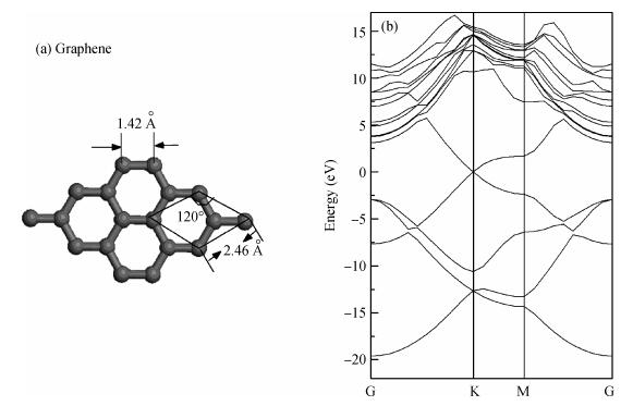
Fig. 1.
(a) The 3 $\times$ 3 graphene supercell with the calculated structural parameters. (b) The band structure for graphene when the band gap is zero.
SEMICONDUCTOR MATERIALS
Gui Yang1, 2, , Yufeng Zhang1 and Xunwang Yan1
Corresponding author: Yang Gui, Email:kuiziyang@126.com
Abstract: The electronic and optical properties of graphene monoxide, a new type of semiconductor material, are theoretically studied by first-principles density functional theory. The calculated band structure shows that graphene monoxide is a semiconductor with a direct band gap of 0.95 eV. The density of states of graphene monoxide and the partial density of states for C and O are given to understand the electronic structure. In addition, we calculate the optical properties of graphene monoxide, including the complex dielectric function, absorption coefficient, complex refractive index, loss-function, reflectivity and conductivity. These results provide a physical basis for potential application in optoelectronic devices.
Keywords: graphene monoxide, electronic band structure, optical property
| [1] |
Novoselov K S, Geim A K, Morozov S V, et al. Two-dimensional gas of massless Dirac fermions in grapheme. Nature (London), 2005, 438:197 doi: 10.1038/nature04233
|
| [2] |
Novoselov K S, Geim A K, Morozov S V, et al. Electric field effect in atomically thin carbon films. Science, 2004, 306:666 doi: 10.1126/science.1102896
|
| [3] |
Zhang Y B, Tan Y W, Stormer H L, et al. Hall effect and Berry's phase in grapheme. Nature, 2005, 438:201 doi: 10.1038/nature04235
|
| [4] |
Meyer J C, Geim A K, Katsnelson M I, et al. The structure of suspended graphene sheets. Nature, 2007, 446:60 doi: 10.1038/nature05545
|
| [5] |
Oostinga J B, Heersche H B, Liu X L, et al. Gate-induced insulating state in bilayer graphene devices. Nature Mater, 2007, 7:151 https://arxiv.org/pdf/0707.2487
|
| [6] |
Rycerz A. Random matrices and quantum chaos in weakly disordered graphene nanoflakes. Phys Rev B, 2012, 85:245424 doi: 10.1103/PhysRevB.85.245424
|
| [7] |
Rasanen E, Rozzi C A, Pittalis S, et al. Electron-electron interactions in artificial graphene. Phys Rev Lett, 2012, 108:246803 doi: 10.1103/PhysRevLett.108.246803
|
| [8] |
Huang B L, Chang M C, Mou C Y. Persistent currents in a graphene ring with armchair edges. J Phys:Condens Matter, 2012, 24:245304 doi: 10.1088/0953-8984/24/24/245304
|
| [9] |
Hung N V, Mazzamuto F, Bournel A, et al. Resonant tunnelling diodes based on graphene/h-BN heterostructure. J Phys D:Appl Phys, 2012, 45:325104 doi: 10.1088/0022-3727/45/32/325104
|
| [10] |
Castro E V, Novoselov K S, Morozov S V, et al. Biased bilayer graphene:semiconductor with a gap tunable by the electric field effect. Phys Rev Lett, 2007, 99:216802 doi: 10.1103/PhysRevLett.99.216802
|
| [11] |
Zhang Y, Tang T T, Girit C, et al. Direct observation of a widely tunable bandgap in bilayer grapheme. Nature (London), 2009, 459:820 doi: 10.1038/nature08105
|
| [12] |
Yang L, Park C H, Son Y W, et al. Quasiparticle energies and band gaps in graphene nanoribbons. Phys Rev Lett, 2007, 99:186801 doi: 10.1103/PhysRevLett.99.186801
|
| [13] |
Han M Y, Özyilmaz B, Zhang Y, et al. Energy band-gap engineering of graphene nanoribbons. Phys Rev Lett, 2007, 98:206805 doi: 10.1103/PhysRevLett.98.206805
|
| [14] |
Li X L, Wang X R, Zhang L, et al. Chemically derived, ultrasmooth graphene nanoribbon semiconductors. Science, 2008, 319:5867, 1229 http://www.doc88.com/p-745821994305.html
|
| [15] |
Wang X R, Ouyang Y J, Li X L, et al. Room-temperature all-semiconducting sub-10-nm graphene nanoribbon field-effect transistors. Phys Rev Lett, 2008, 100:206803 doi: 10.1103/PhysRevLett.100.206803
|
| [16] |
Biel B, Blase X, Triozon F, et al. Anomalous doping effects on charge transport in graphene nanoribbons. Phys Rev Lett, 2009, 102:096803 doi: 10.1103/PhysRevLett.102.096803
|
| [17] |
Yu S, Zheng W, Wang C, et al. Nitrogen/boron doping position dependence of the electronic properties of a triangular grapheme. ACS Nano, 2010, 4:7619 doi: 10.1021/nn102369r
|
| [18] |
Li Y, Zhou Z, Shen P, et al. Spin gapless semiconductor-metal-half-metal properties in nitrogen-doped zigzag graphene nanoribbons. ACS Nano, 2009, 3:1952 doi: 10.1021/nn9003428
|
| [19] |
Lherbier A, Blase X, Niquet Y M, et al. Charge transport in chemically doped 2D grapheme. Phys Rev Lett, 2008, 101:036808 doi: 10.1103/PhysRevLett.101.036808
|
| [20] |
Deng D H, Pan X L, Yu L, et al. Toward N-doped graphene via solvothermal synthesis. Chem Mater, 2011, 23(5):1188 doi: 10.1021/cm102666r
|
| [21] |
Li Y, Zhao Y, Cheng H H, et al. Nitrogen-doped graphene quantum dots with oxygen-rich functional groups. J Am Chem Soc, 2012, 134(1):15 doi: 10.1021/ja206030c
|
| [22] |
Joucken F, Tison Y, Lagoute J, et al. Localized state and charge transfer in nitrogen-doped grapheme. Phys Rev B, 2012, 85:161408(R) doi: 10.1103/PhysRevB.85.161408
|
| [23] |
Xiang H J, Huang B, Li Z Y, et al. Ordered semiconducting nitrogen-graphene alloys. Phys Rev X, 2012, 2:011003 http://adsabs.harvard.edu/abs/2012PhRvX...2a1003X
|
| [24] |
Mkhoyan K A, Contryman A W, Silcox J, et al. Atomic and electronic structure of graphene-oxide. Nano Lett, 2009, 9(3):1058 doi: 10.1021/nl8034256
|
| [25] |
Parka S J, Sukb J W, Anb J, et al. The effect of concentration of graphene nanoplatelets on mechanical and electrical properties of reduced graphene oxide papers. Carbon, 2012, 50(12):4573 doi: 10.1016/j.carbon.2012.05.042
|
| [26] |
Lu G H, Park S, Yu K H, et al. Toward practical gas sensing with highly reduced graphene oxide:a new signal processing method to circumvent run-to-run and device-to-device variations. ACS Nano, 2011, 5:1154 doi: 10.1021/nn102803q
|
| [27] |
Mattson E C, Pu H H, Cui S M, et al. Evidence of nanocrystalline semiconducting graphene monoxide during thermal reduction of graphene oxide in vacuum. ACS Nano, 2011, 5(12):9710 doi: 10.1021/nn203160n
|
| [28] |
Neto A H C, Guinea F, Peres N M R, et al. The electronic properties of grapheme. Rev Mod Phys, 2009, 81:109 doi: 10.1103/RevModPhys.81.109
|
| [29] |
Shen X C. Semiconductor optical properties. Science Press, 1992
|
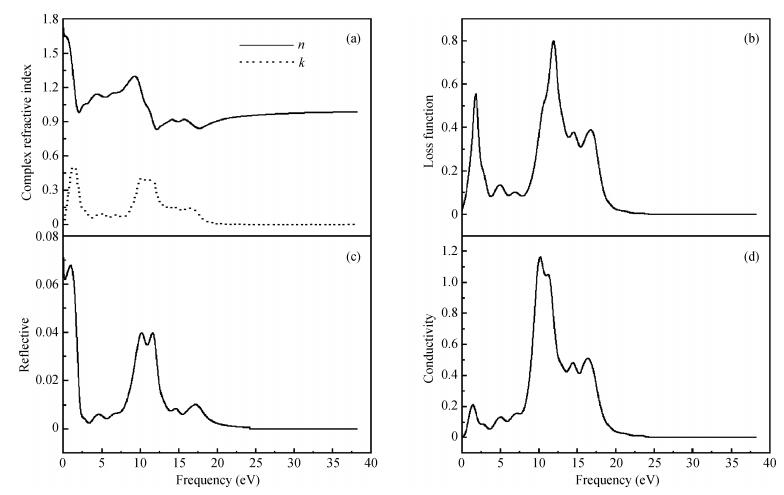
Table 1. Population analysis results of graphene and GMO.

|
| [1] |
Novoselov K S, Geim A K, Morozov S V, et al. Two-dimensional gas of massless Dirac fermions in grapheme. Nature (London), 2005, 438:197 doi: 10.1038/nature04233
|
| [2] |
Novoselov K S, Geim A K, Morozov S V, et al. Electric field effect in atomically thin carbon films. Science, 2004, 306:666 doi: 10.1126/science.1102896
|
| [3] |
Zhang Y B, Tan Y W, Stormer H L, et al. Hall effect and Berry's phase in grapheme. Nature, 2005, 438:201 doi: 10.1038/nature04235
|
| [4] |
Meyer J C, Geim A K, Katsnelson M I, et al. The structure of suspended graphene sheets. Nature, 2007, 446:60 doi: 10.1038/nature05545
|
| [5] |
Oostinga J B, Heersche H B, Liu X L, et al. Gate-induced insulating state in bilayer graphene devices. Nature Mater, 2007, 7:151 https://arxiv.org/pdf/0707.2487
|
| [6] |
Rycerz A. Random matrices and quantum chaos in weakly disordered graphene nanoflakes. Phys Rev B, 2012, 85:245424 doi: 10.1103/PhysRevB.85.245424
|
| [7] |
Rasanen E, Rozzi C A, Pittalis S, et al. Electron-electron interactions in artificial graphene. Phys Rev Lett, 2012, 108:246803 doi: 10.1103/PhysRevLett.108.246803
|
| [8] |
Huang B L, Chang M C, Mou C Y. Persistent currents in a graphene ring with armchair edges. J Phys:Condens Matter, 2012, 24:245304 doi: 10.1088/0953-8984/24/24/245304
|
| [9] |
Hung N V, Mazzamuto F, Bournel A, et al. Resonant tunnelling diodes based on graphene/h-BN heterostructure. J Phys D:Appl Phys, 2012, 45:325104 doi: 10.1088/0022-3727/45/32/325104
|
| [10] |
Castro E V, Novoselov K S, Morozov S V, et al. Biased bilayer graphene:semiconductor with a gap tunable by the electric field effect. Phys Rev Lett, 2007, 99:216802 doi: 10.1103/PhysRevLett.99.216802
|
| [11] |
Zhang Y, Tang T T, Girit C, et al. Direct observation of a widely tunable bandgap in bilayer grapheme. Nature (London), 2009, 459:820 doi: 10.1038/nature08105
|
| [12] |
Yang L, Park C H, Son Y W, et al. Quasiparticle energies and band gaps in graphene nanoribbons. Phys Rev Lett, 2007, 99:186801 doi: 10.1103/PhysRevLett.99.186801
|
| [13] |
Han M Y, Özyilmaz B, Zhang Y, et al. Energy band-gap engineering of graphene nanoribbons. Phys Rev Lett, 2007, 98:206805 doi: 10.1103/PhysRevLett.98.206805
|
| [14] |
Li X L, Wang X R, Zhang L, et al. Chemically derived, ultrasmooth graphene nanoribbon semiconductors. Science, 2008, 319:5867, 1229 http://www.doc88.com/p-745821994305.html
|
| [15] |
Wang X R, Ouyang Y J, Li X L, et al. Room-temperature all-semiconducting sub-10-nm graphene nanoribbon field-effect transistors. Phys Rev Lett, 2008, 100:206803 doi: 10.1103/PhysRevLett.100.206803
|
| [16] |
Biel B, Blase X, Triozon F, et al. Anomalous doping effects on charge transport in graphene nanoribbons. Phys Rev Lett, 2009, 102:096803 doi: 10.1103/PhysRevLett.102.096803
|
| [17] |
Yu S, Zheng W, Wang C, et al. Nitrogen/boron doping position dependence of the electronic properties of a triangular grapheme. ACS Nano, 2010, 4:7619 doi: 10.1021/nn102369r
|
| [18] |
Li Y, Zhou Z, Shen P, et al. Spin gapless semiconductor-metal-half-metal properties in nitrogen-doped zigzag graphene nanoribbons. ACS Nano, 2009, 3:1952 doi: 10.1021/nn9003428
|
| [19] |
Lherbier A, Blase X, Niquet Y M, et al. Charge transport in chemically doped 2D grapheme. Phys Rev Lett, 2008, 101:036808 doi: 10.1103/PhysRevLett.101.036808
|
| [20] |
Deng D H, Pan X L, Yu L, et al. Toward N-doped graphene via solvothermal synthesis. Chem Mater, 2011, 23(5):1188 doi: 10.1021/cm102666r
|
| [21] |
Li Y, Zhao Y, Cheng H H, et al. Nitrogen-doped graphene quantum dots with oxygen-rich functional groups. J Am Chem Soc, 2012, 134(1):15 doi: 10.1021/ja206030c
|
| [22] |
Joucken F, Tison Y, Lagoute J, et al. Localized state and charge transfer in nitrogen-doped grapheme. Phys Rev B, 2012, 85:161408(R) doi: 10.1103/PhysRevB.85.161408
|
| [23] |
Xiang H J, Huang B, Li Z Y, et al. Ordered semiconducting nitrogen-graphene alloys. Phys Rev X, 2012, 2:011003 http://adsabs.harvard.edu/abs/2012PhRvX...2a1003X
|
| [24] |
Mkhoyan K A, Contryman A W, Silcox J, et al. Atomic and electronic structure of graphene-oxide. Nano Lett, 2009, 9(3):1058 doi: 10.1021/nl8034256
|
| [25] |
Parka S J, Sukb J W, Anb J, et al. The effect of concentration of graphene nanoplatelets on mechanical and electrical properties of reduced graphene oxide papers. Carbon, 2012, 50(12):4573 doi: 10.1016/j.carbon.2012.05.042
|
| [26] |
Lu G H, Park S, Yu K H, et al. Toward practical gas sensing with highly reduced graphene oxide:a new signal processing method to circumvent run-to-run and device-to-device variations. ACS Nano, 2011, 5:1154 doi: 10.1021/nn102803q
|
| [27] |
Mattson E C, Pu H H, Cui S M, et al. Evidence of nanocrystalline semiconducting graphene monoxide during thermal reduction of graphene oxide in vacuum. ACS Nano, 2011, 5(12):9710 doi: 10.1021/nn203160n
|
| [28] |
Neto A H C, Guinea F, Peres N M R, et al. The electronic properties of grapheme. Rev Mod Phys, 2009, 81:109 doi: 10.1103/RevModPhys.81.109
|
| [29] |
Shen X C. Semiconductor optical properties. Science Press, 1992
|


Article views: 2779 Times PDF downloads: 15 Times Cited by: 0 Times
Received: 27 January 2013 Revised: 06 March 2013 Online: Published: 01 August 2013
| Citation: |
Gui Yang, Yufeng Zhang, Xunwang Yan. Electronic structure and optical properties of a new type of semiconductor material:graphene monoxide[J]. Journal of Semiconductors, 2013, 34(8): 083004. doi: 10.1088/1674-4926/34/8/083004
****
G Yang, Y F Zhang, X W Yan. Electronic structure and optical properties of a new type of semiconductor material:graphene monoxide[J]. J. Semicond., 2013, 34(8): 083004. doi: 10.1088/1674-4926/34/8/083004.

|
| [1] |
Novoselov K S, Geim A K, Morozov S V, et al. Two-dimensional gas of massless Dirac fermions in grapheme. Nature (London), 2005, 438:197 doi: 10.1038/nature04233
|
| [2] |
Novoselov K S, Geim A K, Morozov S V, et al. Electric field effect in atomically thin carbon films. Science, 2004, 306:666 doi: 10.1126/science.1102896
|
| [3] |
Zhang Y B, Tan Y W, Stormer H L, et al. Hall effect and Berry's phase in grapheme. Nature, 2005, 438:201 doi: 10.1038/nature04235
|
| [4] |
Meyer J C, Geim A K, Katsnelson M I, et al. The structure of suspended graphene sheets. Nature, 2007, 446:60 doi: 10.1038/nature05545
|
| [5] |
Oostinga J B, Heersche H B, Liu X L, et al. Gate-induced insulating state in bilayer graphene devices. Nature Mater, 2007, 7:151 https://arxiv.org/pdf/0707.2487
|
| [6] |
Rycerz A. Random matrices and quantum chaos in weakly disordered graphene nanoflakes. Phys Rev B, 2012, 85:245424 doi: 10.1103/PhysRevB.85.245424
|
| [7] |
Rasanen E, Rozzi C A, Pittalis S, et al. Electron-electron interactions in artificial graphene. Phys Rev Lett, 2012, 108:246803 doi: 10.1103/PhysRevLett.108.246803
|
| [8] |
Huang B L, Chang M C, Mou C Y. Persistent currents in a graphene ring with armchair edges. J Phys:Condens Matter, 2012, 24:245304 doi: 10.1088/0953-8984/24/24/245304
|
| [9] |
Hung N V, Mazzamuto F, Bournel A, et al. Resonant tunnelling diodes based on graphene/h-BN heterostructure. J Phys D:Appl Phys, 2012, 45:325104 doi: 10.1088/0022-3727/45/32/325104
|
| [10] |
Castro E V, Novoselov K S, Morozov S V, et al. Biased bilayer graphene:semiconductor with a gap tunable by the electric field effect. Phys Rev Lett, 2007, 99:216802 doi: 10.1103/PhysRevLett.99.216802
|
| [11] |
Zhang Y, Tang T T, Girit C, et al. Direct observation of a widely tunable bandgap in bilayer grapheme. Nature (London), 2009, 459:820 doi: 10.1038/nature08105
|
| [12] |
Yang L, Park C H, Son Y W, et al. Quasiparticle energies and band gaps in graphene nanoribbons. Phys Rev Lett, 2007, 99:186801 doi: 10.1103/PhysRevLett.99.186801
|
| [13] |
Han M Y, Özyilmaz B, Zhang Y, et al. Energy band-gap engineering of graphene nanoribbons. Phys Rev Lett, 2007, 98:206805 doi: 10.1103/PhysRevLett.98.206805
|
| [14] |
Li X L, Wang X R, Zhang L, et al. Chemically derived, ultrasmooth graphene nanoribbon semiconductors. Science, 2008, 319:5867, 1229 http://www.doc88.com/p-745821994305.html
|
| [15] |
Wang X R, Ouyang Y J, Li X L, et al. Room-temperature all-semiconducting sub-10-nm graphene nanoribbon field-effect transistors. Phys Rev Lett, 2008, 100:206803 doi: 10.1103/PhysRevLett.100.206803
|
| [16] |
Biel B, Blase X, Triozon F, et al. Anomalous doping effects on charge transport in graphene nanoribbons. Phys Rev Lett, 2009, 102:096803 doi: 10.1103/PhysRevLett.102.096803
|
| [17] |
Yu S, Zheng W, Wang C, et al. Nitrogen/boron doping position dependence of the electronic properties of a triangular grapheme. ACS Nano, 2010, 4:7619 doi: 10.1021/nn102369r
|
| [18] |
Li Y, Zhou Z, Shen P, et al. Spin gapless semiconductor-metal-half-metal properties in nitrogen-doped zigzag graphene nanoribbons. ACS Nano, 2009, 3:1952 doi: 10.1021/nn9003428
|
| [19] |
Lherbier A, Blase X, Niquet Y M, et al. Charge transport in chemically doped 2D grapheme. Phys Rev Lett, 2008, 101:036808 doi: 10.1103/PhysRevLett.101.036808
|
| [20] |
Deng D H, Pan X L, Yu L, et al. Toward N-doped graphene via solvothermal synthesis. Chem Mater, 2011, 23(5):1188 doi: 10.1021/cm102666r
|
| [21] |
Li Y, Zhao Y, Cheng H H, et al. Nitrogen-doped graphene quantum dots with oxygen-rich functional groups. J Am Chem Soc, 2012, 134(1):15 doi: 10.1021/ja206030c
|
| [22] |
Joucken F, Tison Y, Lagoute J, et al. Localized state and charge transfer in nitrogen-doped grapheme. Phys Rev B, 2012, 85:161408(R) doi: 10.1103/PhysRevB.85.161408
|
| [23] |
Xiang H J, Huang B, Li Z Y, et al. Ordered semiconducting nitrogen-graphene alloys. Phys Rev X, 2012, 2:011003 http://adsabs.harvard.edu/abs/2012PhRvX...2a1003X
|
| [24] |
Mkhoyan K A, Contryman A W, Silcox J, et al. Atomic and electronic structure of graphene-oxide. Nano Lett, 2009, 9(3):1058 doi: 10.1021/nl8034256
|
| [25] |
Parka S J, Sukb J W, Anb J, et al. The effect of concentration of graphene nanoplatelets on mechanical and electrical properties of reduced graphene oxide papers. Carbon, 2012, 50(12):4573 doi: 10.1016/j.carbon.2012.05.042
|
| [26] |
Lu G H, Park S, Yu K H, et al. Toward practical gas sensing with highly reduced graphene oxide:a new signal processing method to circumvent run-to-run and device-to-device variations. ACS Nano, 2011, 5:1154 doi: 10.1021/nn102803q
|
| [27] |
Mattson E C, Pu H H, Cui S M, et al. Evidence of nanocrystalline semiconducting graphene monoxide during thermal reduction of graphene oxide in vacuum. ACS Nano, 2011, 5(12):9710 doi: 10.1021/nn203160n
|
| [28] |
Neto A H C, Guinea F, Peres N M R, et al. The electronic properties of grapheme. Rev Mod Phys, 2009, 81:109 doi: 10.1103/RevModPhys.81.109
|
| [29] |
Shen X C. Semiconductor optical properties. Science Press, 1992
|

 WeChat ID
Journal of Semiconductors © 2017 All Rights Reserved 京ICP备05085259号-2

 DownLoad:

