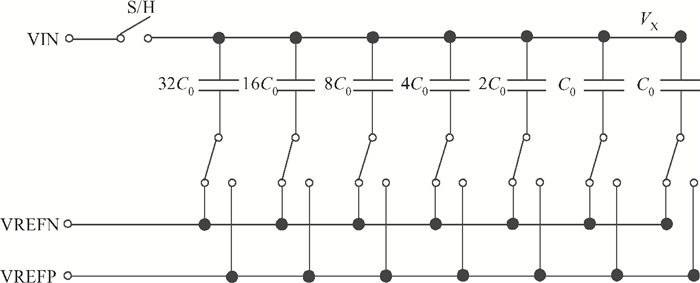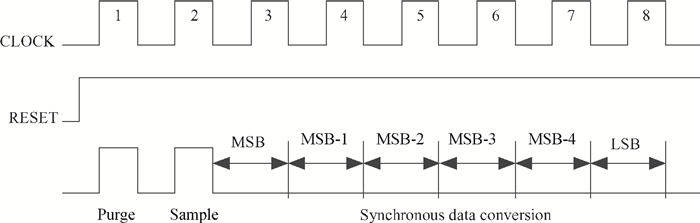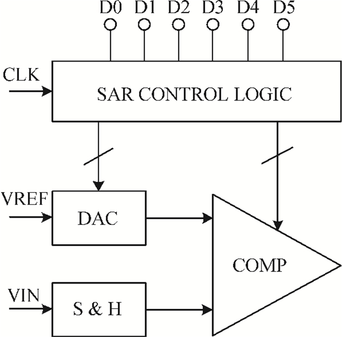
Fig. 1.
Typical block diagram of 6-bit SAR ADC.
SEMICONDUCTOR INTEGRATED CIRCUITS
Xue Han, Hua Fan, Qi Wei and Huazhong Yang
Corresponding author: Han Xue, Email:snowhx1988@163.com
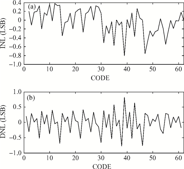
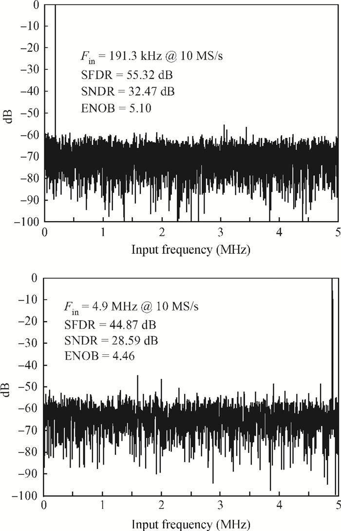
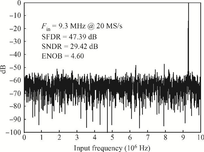
Abstract: This paper presents a 6-bit 20-MS/s high spurious-free dynamic range (SFDR) and low power successive approximation register analog to digital converter (SAR ADC) for the radio-frequency (RF) transceiver front-end, especially for wireless sensor network (WSN) applications. This ADC adopts the modified common-centroid symmetry layout and the successive approximation register reset circuit to improve the linearity and dynamic range. Prototyped in a 0.18-μm 1P6M CMOS technology, the ADC performs a peak SFDR of 55.32 dB and effective number of bits (ENOB) of 5.1 bit for 10 MS/s. At the sample rate of 20 MS/s and the Nyquist input frequency, the 47.39-dB SFDR and 4.6-ENOB are achieved. The differential nonlinearity (DNL) is less than 0.83 LSB and the integral nonlinearity (INL) is less than 0.82 LSB. The experimental results indicate that this SAR ADC consumes a total of 522 μW power and occupies 0.98 mm2.
Key words: analog to digital converter, common-centroid symmetry layout, successive approximation register, time domain comparator
| [1] |
Alpman E, Lakdawala H, Carley L R, et al. A 1.1 V 50 mW 2.5 GS/s 7 b time-interleaved C-2C SAR ADC in 45 nm LP digital CMOS. IEEE ISSCC Dig Tech Papers, 2009:65
|
| [2] |
Van Elzakker M, van Tuijl E, Geraedts P, et al. A 1.9μ W 4.4 fJ/conversion-step 10 b 1 MS/s charge-redistribution ADC. IEEE ISSCC Dig Tech Papers, 2008:244
|
| [3] |
Wei H G, Chan C H, Chio U F, et al. An 8-b 400-MS/s 2-b-per-cycle SAR ADC with resistive DAC. IEEE J Solid-State Circuits, 2012, 47(11):2763 doi: 10.1109/JSSC.2012.2214181
|
| [4] |
Chen S W M, Brodersen R W. A 6 b 600 MS/s 5.3 mW asynchronous ADC in 0.13μm CMOS. IEEE ISSCC Dig Tech Papers, 2006:574
|
| [5] |
Razavi B. Principles of data conversion system design. New York:Wiley-IEEE Press, 1995 http://ieeexplore.ieee.org/xpl/bkabstractplus.jsp?bkn=5264233
|
| [6] |
Lin Y, Chang S, Liu Y, et al. A 5 b 800 MS/s 2 mW asynchronous binary-search ADC in 65 nm CMOS. IEEE ISSCC Dig Tech Papers, 2009:80
|
| [7] |
Agnes A, Bonizzoni E, Malcovati P, et al. A 9.4-ENOB 1 V 3.8μ W 100 kS/s SAR ADC with time-domain comparator. IEEE International Solid-State Circuits Conference (ISSCC), 2008:246
|
| [8] |
Lin Y Z, Chang S J, Liu Y T, et al. An asynchronous binary-search ADC architecture with a reduced comparator count. IEEE Trans Circuits Syst Ⅰ, 2010, 57(8):1829 doi: 10.1109/TCSI.2009.2037403
|
| [9] |
Kobenge S B. Circuit techniques for low-voltage low-power successive approximation register analog-to-digital converter. PhD Thesis, Tsinghua University, 2010
|
| [10] |
Gustavsson M, Wikner J J, Tan N N. CMOS data converters for communications. Boston:Kluwer Academic Publishers, 2000 http://www.diva-portal.org/smash/record.jsf?pid=diva2%3A440945&dswid=-7158
|
| [11] |
Colleran W T. A 10-bit 100-MS/s A/D converter using folding, interpolating, and analog encoding. PhD Thesis, University of California, Los Angeles, CA, 1993
|
| [12] |
Pan H, Segami M, Choi M, et al. A 3.3-V 12-b 50-MS/s A/D converter in 0.6-μm CMOS with over 80-dB SFDR. IEEE J Solid-State Circuits, 2000, 35(12):1769 doi: 10.1109/4.890290
|
| [13] |
Kobenge S B, Yang H. A novel low power time-mode comparator for successive approximation register ADC. IEICE Electronics Express, 2009, 6(16):1155 doi: 10.1587/elex.6.1155
|
| [14] |
Anderson T. Optimum control logic for successive approximation analog-to-digital converters. Deep Space Network Progress Report, 1972, 13:168
|
| [15] |
Ginsburg B P. Energy-efficient analog-to-digital conversion for ultra-wideband radio. PhD Thesis, MIT, 2007:138 http://dspace.mit.edu/handle/1721.1/42231
|
| [16] |
Liu W, Huang P, Chiu Y. A 12-bit, 45-MS/s, 3-mW redun-dant successive-approximation-register analog-to-digital con-verter with digital calibration. IEEE J Solid-State Circuits, 2011, 46(11):2661 doi: 10.1109/JSSC.2011.2163556
|
| [17] |
Taillefer C. Analog-to-digital conversion via time-mode signal processing. PhD Thesis, McGill University, 2007 https://dl.acm.org/citation.cfm?id=1713982
|
| [18] |
Cao Z, Yan S, Li Y. A 32 mW 1.25 GS/s 6 b 2 b/step SAR ADC in 0.13μm CMOS. IEEE J Solid-State Circuits, 2009, 44(3):862 doi: 10.1109/JSSC.2008.2012329
|
| [19] |
Fan Hua, Wei Qi, Kebenge Sekedi Bomeh, et al. An 8-bit 180-kS/s differential SAR ADC with a time-domain comparator and 7.97-SFDR. Journal of Semiconductors, 2010, 31(9):095011 doi: 10.1088/1674-4926/31/9/095011
|
| [20] |
Liu Liyuan, Li Dongmei, Chen Liangdong, et al. A low power 8-bit successive approximation register A/D for a wireless body sensor node. Journal of Semiconductors, 2010, 31(6):035002 http://www.jos.ac.cn/bdtxbcn/ch/reader/view_abstract.aspx?file_no=09111202&flag=1
|
| [21] |
Ginsburg B P, Chandrakasan A P. 500-MS/s 5-bit ADC in 65-nm CMOS with split capacitor array DAC. IEEE J Solid-State Circuits, 2007, 42(4):739 doi: 10.1109/JSSC.2007.892169
|
| [22] |
Yang J, Naing T L, Brodersen R W. A 1 GS/s 6 bit 6.7 mW successive approximation ADC using asynchronous processing. IEEE J Solid-State Circuits, 2010, 45(8):1469 doi: 10.1109/JSSC.2010.2048139
|
| [23] |
Wong S S, Chio U F, Chan C H, et al. A 4.8-bit ENOB 5-bit 500 MS/s binary-search ADC with minimized number of comparators. IEEE ASSCC, 2011:73
|
| [24] |
Ali A M A, Dillon C, Sneed R, et al. A 14-bit 125 MS/s IF/RF sampling pipelined ADC with 100 dB SFDR and 50 fs jitter. IEEE J Solid-State Circuits, 2006, 41(8):1846 doi: 10.1109/JSSC.2006.875291
|
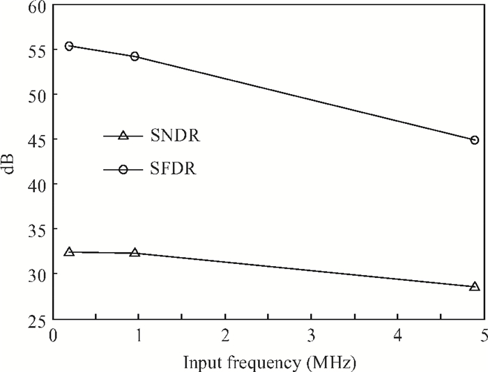
Table 1. Summary of experimental performance and comparison with several designs.

|
| [1] |
Alpman E, Lakdawala H, Carley L R, et al. A 1.1 V 50 mW 2.5 GS/s 7 b time-interleaved C-2C SAR ADC in 45 nm LP digital CMOS. IEEE ISSCC Dig Tech Papers, 2009:65
|
| [2] |
Van Elzakker M, van Tuijl E, Geraedts P, et al. A 1.9μ W 4.4 fJ/conversion-step 10 b 1 MS/s charge-redistribution ADC. IEEE ISSCC Dig Tech Papers, 2008:244
|
| [3] |
Wei H G, Chan C H, Chio U F, et al. An 8-b 400-MS/s 2-b-per-cycle SAR ADC with resistive DAC. IEEE J Solid-State Circuits, 2012, 47(11):2763 doi: 10.1109/JSSC.2012.2214181
|
| [4] |
Chen S W M, Brodersen R W. A 6 b 600 MS/s 5.3 mW asynchronous ADC in 0.13μm CMOS. IEEE ISSCC Dig Tech Papers, 2006:574
|
| [5] |
Razavi B. Principles of data conversion system design. New York:Wiley-IEEE Press, 1995 http://ieeexplore.ieee.org/xpl/bkabstractplus.jsp?bkn=5264233
|
| [6] |
Lin Y, Chang S, Liu Y, et al. A 5 b 800 MS/s 2 mW asynchronous binary-search ADC in 65 nm CMOS. IEEE ISSCC Dig Tech Papers, 2009:80
|
| [7] |
Agnes A, Bonizzoni E, Malcovati P, et al. A 9.4-ENOB 1 V 3.8μ W 100 kS/s SAR ADC with time-domain comparator. IEEE International Solid-State Circuits Conference (ISSCC), 2008:246
|
| [8] |
Lin Y Z, Chang S J, Liu Y T, et al. An asynchronous binary-search ADC architecture with a reduced comparator count. IEEE Trans Circuits Syst Ⅰ, 2010, 57(8):1829 doi: 10.1109/TCSI.2009.2037403
|
| [9] |
Kobenge S B. Circuit techniques for low-voltage low-power successive approximation register analog-to-digital converter. PhD Thesis, Tsinghua University, 2010
|
| [10] |
Gustavsson M, Wikner J J, Tan N N. CMOS data converters for communications. Boston:Kluwer Academic Publishers, 2000 http://www.diva-portal.org/smash/record.jsf?pid=diva2%3A440945&dswid=-7158
|
| [11] |
Colleran W T. A 10-bit 100-MS/s A/D converter using folding, interpolating, and analog encoding. PhD Thesis, University of California, Los Angeles, CA, 1993
|
| [12] |
Pan H, Segami M, Choi M, et al. A 3.3-V 12-b 50-MS/s A/D converter in 0.6-μm CMOS with over 80-dB SFDR. IEEE J Solid-State Circuits, 2000, 35(12):1769 doi: 10.1109/4.890290
|
| [13] |
Kobenge S B, Yang H. A novel low power time-mode comparator for successive approximation register ADC. IEICE Electronics Express, 2009, 6(16):1155 doi: 10.1587/elex.6.1155
|
| [14] |
Anderson T. Optimum control logic for successive approximation analog-to-digital converters. Deep Space Network Progress Report, 1972, 13:168
|
| [15] |
Ginsburg B P. Energy-efficient analog-to-digital conversion for ultra-wideband radio. PhD Thesis, MIT, 2007:138 http://dspace.mit.edu/handle/1721.1/42231
|
| [16] |
Liu W, Huang P, Chiu Y. A 12-bit, 45-MS/s, 3-mW redun-dant successive-approximation-register analog-to-digital con-verter with digital calibration. IEEE J Solid-State Circuits, 2011, 46(11):2661 doi: 10.1109/JSSC.2011.2163556
|
| [17] |
Taillefer C. Analog-to-digital conversion via time-mode signal processing. PhD Thesis, McGill University, 2007 https://dl.acm.org/citation.cfm?id=1713982
|
| [18] |
Cao Z, Yan S, Li Y. A 32 mW 1.25 GS/s 6 b 2 b/step SAR ADC in 0.13μm CMOS. IEEE J Solid-State Circuits, 2009, 44(3):862 doi: 10.1109/JSSC.2008.2012329
|
| [19] |
Fan Hua, Wei Qi, Kebenge Sekedi Bomeh, et al. An 8-bit 180-kS/s differential SAR ADC with a time-domain comparator and 7.97-SFDR. Journal of Semiconductors, 2010, 31(9):095011 doi: 10.1088/1674-4926/31/9/095011
|
| [20] |
Liu Liyuan, Li Dongmei, Chen Liangdong, et al. A low power 8-bit successive approximation register A/D for a wireless body sensor node. Journal of Semiconductors, 2010, 31(6):035002 http://www.jos.ac.cn/bdtxbcn/ch/reader/view_abstract.aspx?file_no=09111202&flag=1
|
| [21] |
Ginsburg B P, Chandrakasan A P. 500-MS/s 5-bit ADC in 65-nm CMOS with split capacitor array DAC. IEEE J Solid-State Circuits, 2007, 42(4):739 doi: 10.1109/JSSC.2007.892169
|
| [22] |
Yang J, Naing T L, Brodersen R W. A 1 GS/s 6 bit 6.7 mW successive approximation ADC using asynchronous processing. IEEE J Solid-State Circuits, 2010, 45(8):1469 doi: 10.1109/JSSC.2010.2048139
|
| [23] |
Wong S S, Chio U F, Chan C H, et al. A 4.8-bit ENOB 5-bit 500 MS/s binary-search ADC with minimized number of comparators. IEEE ASSCC, 2011:73
|
| [24] |
Ali A M A, Dillon C, Sneed R, et al. A 14-bit 125 MS/s IF/RF sampling pipelined ADC with 100 dB SFDR and 50 fs jitter. IEEE J Solid-State Circuits, 2006, 41(8):1846 doi: 10.1109/JSSC.2006.875291
|


Article views: 2908 Times PDF downloads: 32 Times Cited by: 0 Times
Received: 14 December 2012 Revised: 23 January 2013 Online: Published: 01 August 2013
| Citation: |
Xue Han, Hua Fan, Qi Wei, Huazhong Yang. A high SFDR 6-bit 20-MS/s SAR ADC based on time-domain comparator[J]. Journal of Semiconductors, 2013, 34(8): 085008. doi: 10.1088/1674-4926/34/8/085008
****
X Han, H Fan, Q Wei, H Z Yang. A high SFDR 6-bit 20-MS/s SAR ADC based on time-domain comparator[J]. J. Semicond., 2013, 34(8): 085008. doi: 10.1088/1674-4926/34/8/085008.

|
| [1] |
Alpman E, Lakdawala H, Carley L R, et al. A 1.1 V 50 mW 2.5 GS/s 7 b time-interleaved C-2C SAR ADC in 45 nm LP digital CMOS. IEEE ISSCC Dig Tech Papers, 2009:65
|
| [2] |
Van Elzakker M, van Tuijl E, Geraedts P, et al. A 1.9μ W 4.4 fJ/conversion-step 10 b 1 MS/s charge-redistribution ADC. IEEE ISSCC Dig Tech Papers, 2008:244
|
| [3] |
Wei H G, Chan C H, Chio U F, et al. An 8-b 400-MS/s 2-b-per-cycle SAR ADC with resistive DAC. IEEE J Solid-State Circuits, 2012, 47(11):2763 doi: 10.1109/JSSC.2012.2214181
|
| [4] |
Chen S W M, Brodersen R W. A 6 b 600 MS/s 5.3 mW asynchronous ADC in 0.13μm CMOS. IEEE ISSCC Dig Tech Papers, 2006:574
|
| [5] |
Razavi B. Principles of data conversion system design. New York:Wiley-IEEE Press, 1995 http://ieeexplore.ieee.org/xpl/bkabstractplus.jsp?bkn=5264233
|
| [6] |
Lin Y, Chang S, Liu Y, et al. A 5 b 800 MS/s 2 mW asynchronous binary-search ADC in 65 nm CMOS. IEEE ISSCC Dig Tech Papers, 2009:80
|
| [7] |
Agnes A, Bonizzoni E, Malcovati P, et al. A 9.4-ENOB 1 V 3.8μ W 100 kS/s SAR ADC with time-domain comparator. IEEE International Solid-State Circuits Conference (ISSCC), 2008:246
|
| [8] |
Lin Y Z, Chang S J, Liu Y T, et al. An asynchronous binary-search ADC architecture with a reduced comparator count. IEEE Trans Circuits Syst Ⅰ, 2010, 57(8):1829 doi: 10.1109/TCSI.2009.2037403
|
| [9] |
Kobenge S B. Circuit techniques for low-voltage low-power successive approximation register analog-to-digital converter. PhD Thesis, Tsinghua University, 2010
|
| [10] |
Gustavsson M, Wikner J J, Tan N N. CMOS data converters for communications. Boston:Kluwer Academic Publishers, 2000 http://www.diva-portal.org/smash/record.jsf?pid=diva2%3A440945&dswid=-7158
|
| [11] |
Colleran W T. A 10-bit 100-MS/s A/D converter using folding, interpolating, and analog encoding. PhD Thesis, University of California, Los Angeles, CA, 1993
|
| [12] |
Pan H, Segami M, Choi M, et al. A 3.3-V 12-b 50-MS/s A/D converter in 0.6-μm CMOS with over 80-dB SFDR. IEEE J Solid-State Circuits, 2000, 35(12):1769 doi: 10.1109/4.890290
|
| [13] |
Kobenge S B, Yang H. A novel low power time-mode comparator for successive approximation register ADC. IEICE Electronics Express, 2009, 6(16):1155 doi: 10.1587/elex.6.1155
|
| [14] |
Anderson T. Optimum control logic for successive approximation analog-to-digital converters. Deep Space Network Progress Report, 1972, 13:168
|
| [15] |
Ginsburg B P. Energy-efficient analog-to-digital conversion for ultra-wideband radio. PhD Thesis, MIT, 2007:138 http://dspace.mit.edu/handle/1721.1/42231
|
| [16] |
Liu W, Huang P, Chiu Y. A 12-bit, 45-MS/s, 3-mW redun-dant successive-approximation-register analog-to-digital con-verter with digital calibration. IEEE J Solid-State Circuits, 2011, 46(11):2661 doi: 10.1109/JSSC.2011.2163556
|
| [17] |
Taillefer C. Analog-to-digital conversion via time-mode signal processing. PhD Thesis, McGill University, 2007 https://dl.acm.org/citation.cfm?id=1713982
|
| [18] |
Cao Z, Yan S, Li Y. A 32 mW 1.25 GS/s 6 b 2 b/step SAR ADC in 0.13μm CMOS. IEEE J Solid-State Circuits, 2009, 44(3):862 doi: 10.1109/JSSC.2008.2012329
|
| [19] |
Fan Hua, Wei Qi, Kebenge Sekedi Bomeh, et al. An 8-bit 180-kS/s differential SAR ADC with a time-domain comparator and 7.97-SFDR. Journal of Semiconductors, 2010, 31(9):095011 doi: 10.1088/1674-4926/31/9/095011
|
| [20] |
Liu Liyuan, Li Dongmei, Chen Liangdong, et al. A low power 8-bit successive approximation register A/D for a wireless body sensor node. Journal of Semiconductors, 2010, 31(6):035002 http://www.jos.ac.cn/bdtxbcn/ch/reader/view_abstract.aspx?file_no=09111202&flag=1
|
| [21] |
Ginsburg B P, Chandrakasan A P. 500-MS/s 5-bit ADC in 65-nm CMOS with split capacitor array DAC. IEEE J Solid-State Circuits, 2007, 42(4):739 doi: 10.1109/JSSC.2007.892169
|
| [22] |
Yang J, Naing T L, Brodersen R W. A 1 GS/s 6 bit 6.7 mW successive approximation ADC using asynchronous processing. IEEE J Solid-State Circuits, 2010, 45(8):1469 doi: 10.1109/JSSC.2010.2048139
|
| [23] |
Wong S S, Chio U F, Chan C H, et al. A 4.8-bit ENOB 5-bit 500 MS/s binary-search ADC with minimized number of comparators. IEEE ASSCC, 2011:73
|
| [24] |
Ali A M A, Dillon C, Sneed R, et al. A 14-bit 125 MS/s IF/RF sampling pipelined ADC with 100 dB SFDR and 50 fs jitter. IEEE J Solid-State Circuits, 2006, 41(8):1846 doi: 10.1109/JSSC.2006.875291
|

 WeChat ID
Journal of Semiconductors © 2017 All Rights Reserved 京ICP备05085259号-2

 DownLoad: