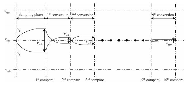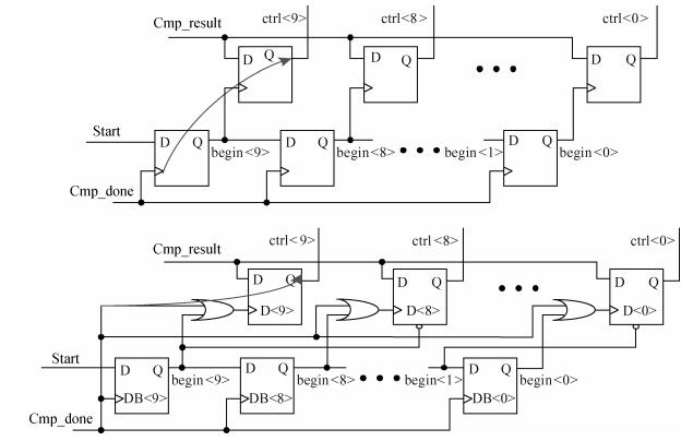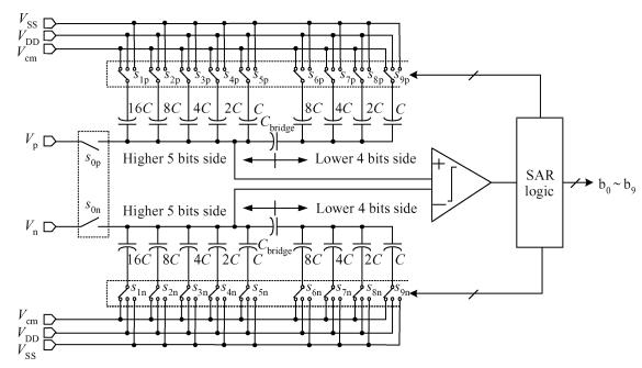
Fig. 1.
SAR ADC architecture.
SEMICONDUCTOR INTEGRATED CIRCUITS
Jun Ma, Yawei Guo, Yue Wu, Xu Cheng and Xiaoyang Zeng
Corresponding author: Cheng Xu, Email:chengxu@fudan.edu.cn
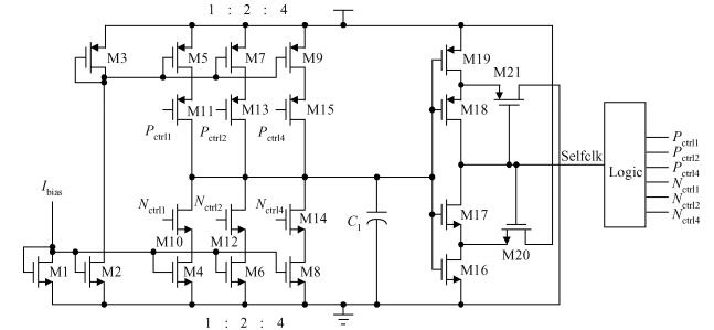
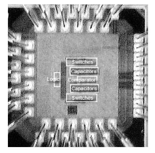
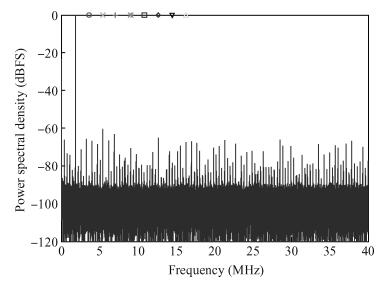
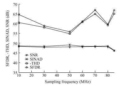
Abstract: This paper presents a 10-bit 80-MS/s successive approximation register (SAR) analog-to-digital converter (ADC) suitable for integration in a system on a chip (SoC). By using the top-plate-sample switching scheme and a split capacitive array structure, the total capacitance is dramatically reduced which leads to low power and high speed. Since the split structure makes the capacitive array highly sensitive to parasitic capacitance, a three-row layout method is applied to the layout design. To overcome the charge leakage in the nanometer process, a special input stage is proposed in the comparator. As 80 MS/s sampling rate for a 10-bit SAR ADC results in around 1 GHz logic control clock, and a tunable clock generator is implemented. The prototype was fabricated in 65 nm 1P9M (one-poly-nine-metal) GP (general purpose) CMOS technology. Measurement results show a peak signal-to-noise and distortion ratio (SINAD) of 48.3 dB and 1.6 mW total power consumption with a figure of merit (FOM) of 94.8 fJ/conversion-step.
Keywords: successive approximation register, analog-to-digital converter, split structure, leakage current
| [1] |
Ma J, Guo Y, Li L, et al. A low power 10-bit 100-MS/s SAR ADC in 65 nm CMOS. IEEE 9th International Conference on ASIC (ASICON), 2011: 484
|
| [2] |
Liu C C, Chang S J, Huang G Y, et al. A 10-bit 50-MS/s SAR ADC with a monotonic capacitor switching procedure. IEEE J Solid-State Circuits, 2010, 45(4):731 doi: 10.1109/JSSC.2010.2042254
|
| [3] |
Zhu Y, Chan C H, Chio U F, et al. A 10-bit 100-MS/s reference-free SAR ADC in 90 nm CMOS. IEEE J Solid-State Circuits, 2010, 45(6):1111 doi: 10.1109/JSSC.2010.2048498
|
| [4] |
McCreary J L, Gray P R. ALL-MOS charge redistribution analog-to-digital conversion techniques-part Ⅰ. IEEE J Solid-State Circuits, 1975, 10(6):371 doi: 10.1109/JSSC.1975.1050629
|
| [5] |
Ginsburg B P, Chandrakasan A P. An energy-efficient charge recycling approach for a SAR converter with capacitive DAC. IEEE International Symposium on ISCAS, 2005: 184
|
| [6] |
Chen Y, Zhu X, Tamura H, et al. Split capacitor DAC mismatch calibration in successive approximation ADC. IEEE Custom Integrated Circuits Conference, 2009: 279
|
| [7] |
Nuzzo P, Bernardinis F D, Terreni P, et al. Noise analysis of regenerative comparators for reconfigurable ADC architectures. IEEE Transactions on Circuits and Systems Ⅰ:Regular Papers, 2008, 55(6):1441 doi: 10.1109/TCSI.2008.917991
|
| [8] |
Chen Lijie, Zhou Yumei, Wei Baoyue. A 10-bit 50-MS/s subsampling pipelined ADC based on SMDAC and opamp sharing. Journal of Semiconductors, 2010, 31(11):115006 doi: 10.1088/1674-4926/31/11/115006
|
| [9] |
Tong Xingyuan, Chen Jianming, Zhu Zhangming, et al. A high performance 90 nm CMOS SAR ADC with hybrid architecture. Journal of Semiconductors, 2010, 31(1):015002 doi: 10.1088/1674-4926/31/1/015002
|
| [10] |
Yang Siyu, Zhang Hui, Fu Wenhui, et al. A low power 12-bit 200-kS/s SAR ADC with a differential time domain comparator. Journal of Semiconductors, 2011, 32(3):035002 doi: 10.1088/1674-4926/32/3/035002
|
| [11] |
Qiao Ning, Zhang Guoquan, Yang Bo, et al. A 10-bit 50-MS/s reference-free low power SAR ADC in 0.18-μm SOI CMOS technology. Journal of Semiconductors, 2012, 33(9):095005 doi: 10.1088/1674-4926/33/9/095005
|
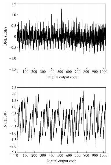
Table 1. Summary of measurement performance.

|
Table 2. Comparison with some previous works.

|
| [1] |
Ma J, Guo Y, Li L, et al. A low power 10-bit 100-MS/s SAR ADC in 65 nm CMOS. IEEE 9th International Conference on ASIC (ASICON), 2011: 484
|
| [2] |
Liu C C, Chang S J, Huang G Y, et al. A 10-bit 50-MS/s SAR ADC with a monotonic capacitor switching procedure. IEEE J Solid-State Circuits, 2010, 45(4):731 doi: 10.1109/JSSC.2010.2042254
|
| [3] |
Zhu Y, Chan C H, Chio U F, et al. A 10-bit 100-MS/s reference-free SAR ADC in 90 nm CMOS. IEEE J Solid-State Circuits, 2010, 45(6):1111 doi: 10.1109/JSSC.2010.2048498
|
| [4] |
McCreary J L, Gray P R. ALL-MOS charge redistribution analog-to-digital conversion techniques-part Ⅰ. IEEE J Solid-State Circuits, 1975, 10(6):371 doi: 10.1109/JSSC.1975.1050629
|
| [5] |
Ginsburg B P, Chandrakasan A P. An energy-efficient charge recycling approach for a SAR converter with capacitive DAC. IEEE International Symposium on ISCAS, 2005: 184
|
| [6] |
Chen Y, Zhu X, Tamura H, et al. Split capacitor DAC mismatch calibration in successive approximation ADC. IEEE Custom Integrated Circuits Conference, 2009: 279
|
| [7] |
Nuzzo P, Bernardinis F D, Terreni P, et al. Noise analysis of regenerative comparators for reconfigurable ADC architectures. IEEE Transactions on Circuits and Systems Ⅰ:Regular Papers, 2008, 55(6):1441 doi: 10.1109/TCSI.2008.917991
|
| [8] |
Chen Lijie, Zhou Yumei, Wei Baoyue. A 10-bit 50-MS/s subsampling pipelined ADC based on SMDAC and opamp sharing. Journal of Semiconductors, 2010, 31(11):115006 doi: 10.1088/1674-4926/31/11/115006
|
| [9] |
Tong Xingyuan, Chen Jianming, Zhu Zhangming, et al. A high performance 90 nm CMOS SAR ADC with hybrid architecture. Journal of Semiconductors, 2010, 31(1):015002 doi: 10.1088/1674-4926/31/1/015002
|
| [10] |
Yang Siyu, Zhang Hui, Fu Wenhui, et al. A low power 12-bit 200-kS/s SAR ADC with a differential time domain comparator. Journal of Semiconductors, 2011, 32(3):035002 doi: 10.1088/1674-4926/32/3/035002
|
| [11] |
Qiao Ning, Zhang Guoquan, Yang Bo, et al. A 10-bit 50-MS/s reference-free low power SAR ADC in 0.18-μm SOI CMOS technology. Journal of Semiconductors, 2012, 33(9):095005 doi: 10.1088/1674-4926/33/9/095005
|


Article views: 3577 Times PDF downloads: 71 Times Cited by: 0 Times
Received: 16 January 2013 Revised: 19 March 2013 Online: Published: 01 August 2013
| Citation: |
Jun Ma, Yawei Guo, Yue Wu, Xu Cheng, Xiaoyang Zeng. A 1-V 10-bit 80-MS/s 1.6-mW SAR ADC in 65-nm GP CMOS[J]. Journal of Semiconductors, 2013, 34(8): 085014. doi: 10.1088/1674-4926/34/8/085014
****
J Ma, Y W Guo, Y Wu, X Cheng, X Y Zeng. A 1-V 10-bit 80-MS/s 1.6-mW SAR ADC in 65-nm GP CMOS[J]. J. Semicond., 2013, 34(8): 085014. doi: 10.1088/1674-4926/34/8/085014.

|
| [1] |
Ma J, Guo Y, Li L, et al. A low power 10-bit 100-MS/s SAR ADC in 65 nm CMOS. IEEE 9th International Conference on ASIC (ASICON), 2011: 484
|
| [2] |
Liu C C, Chang S J, Huang G Y, et al. A 10-bit 50-MS/s SAR ADC with a monotonic capacitor switching procedure. IEEE J Solid-State Circuits, 2010, 45(4):731 doi: 10.1109/JSSC.2010.2042254
|
| [3] |
Zhu Y, Chan C H, Chio U F, et al. A 10-bit 100-MS/s reference-free SAR ADC in 90 nm CMOS. IEEE J Solid-State Circuits, 2010, 45(6):1111 doi: 10.1109/JSSC.2010.2048498
|
| [4] |
McCreary J L, Gray P R. ALL-MOS charge redistribution analog-to-digital conversion techniques-part Ⅰ. IEEE J Solid-State Circuits, 1975, 10(6):371 doi: 10.1109/JSSC.1975.1050629
|
| [5] |
Ginsburg B P, Chandrakasan A P. An energy-efficient charge recycling approach for a SAR converter with capacitive DAC. IEEE International Symposium on ISCAS, 2005: 184
|
| [6] |
Chen Y, Zhu X, Tamura H, et al. Split capacitor DAC mismatch calibration in successive approximation ADC. IEEE Custom Integrated Circuits Conference, 2009: 279
|
| [7] |
Nuzzo P, Bernardinis F D, Terreni P, et al. Noise analysis of regenerative comparators for reconfigurable ADC architectures. IEEE Transactions on Circuits and Systems Ⅰ:Regular Papers, 2008, 55(6):1441 doi: 10.1109/TCSI.2008.917991
|
| [8] |
Chen Lijie, Zhou Yumei, Wei Baoyue. A 10-bit 50-MS/s subsampling pipelined ADC based on SMDAC and opamp sharing. Journal of Semiconductors, 2010, 31(11):115006 doi: 10.1088/1674-4926/31/11/115006
|
| [9] |
Tong Xingyuan, Chen Jianming, Zhu Zhangming, et al. A high performance 90 nm CMOS SAR ADC with hybrid architecture. Journal of Semiconductors, 2010, 31(1):015002 doi: 10.1088/1674-4926/31/1/015002
|
| [10] |
Yang Siyu, Zhang Hui, Fu Wenhui, et al. A low power 12-bit 200-kS/s SAR ADC with a differential time domain comparator. Journal of Semiconductors, 2011, 32(3):035002 doi: 10.1088/1674-4926/32/3/035002
|
| [11] |
Qiao Ning, Zhang Guoquan, Yang Bo, et al. A 10-bit 50-MS/s reference-free low power SAR ADC in 0.18-μm SOI CMOS technology. Journal of Semiconductors, 2012, 33(9):095005 doi: 10.1088/1674-4926/33/9/095005
|

 WeChat ID
Journal of Semiconductors © 2017 All Rights Reserved 京ICP备05085259号-2

 DownLoad: