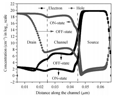
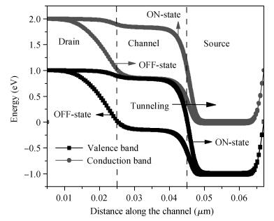
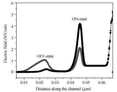
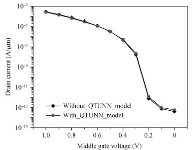
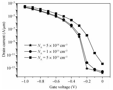
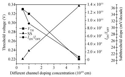
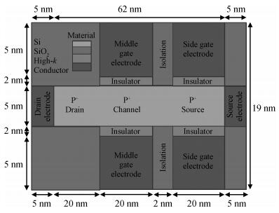
| [1] |
Gundapaneni S, Bajaj M, Pandey R K, et al. Effect of band-to-band tunneling on junctionless transistors. IEEE Trans Electron Devices, 2012, 59:1023 doi: 10.1109/TED.2012.2185800 |
| [2] |
Lilienfeld J E. Method and apparatus for controlling electric current. US Patent, No. 1745175, Oct. 22, 1925
|
| [3] |
Colinge J P, Lee C W, Afzalian A, et al. Nanowire transistors without junctions. Nat Nanotechnol, 2010, 5:225 doi: 10.1038/nnano.2010.15 |
| [4] |
Lee C W, Afzalian A, Akhavan N D, et al. Junctionless multigate field-effect transistor. Appl Phys Lett, 2009, 94:053511 doi: 10.1063/1.3079411 |
| [5] |
Colinge J P, Kranti A, Yan R, et al. Junctionless nanowire transistor (JNT):properties and design guidelines. Solid-State Electron, 2011, 65/66:33
|
| [6] |
Park C H, Ko M D, Kim K H, et al. Electrical characteristics of 20-nm junctionless Si nanowire transistors. Solid-State Electron, 2012, 73:7 doi: 10.1016/j.sse.2011.11.032 |
| [7] |
Lee C W, Ferain I, Afzalian A, et al. Performance estimation of junctionless multigate transistors. Solid-State Electron, 2010, 54:97 doi: 10.1016/j.sse.2009.12.003 |
| [8] |
Leung G, Chui C O. Variability impact of random dopant fluctuation on nanoscale junctionless FinFETs. IEEE Electron Device Lett, 2012, 33:767 doi: 10.1109/LED.2012.2191931 |
| [9] |
Akhavan N D, Ferain I, Razavi P, et al. Random dopant variation in junctionless nanowire transistors. IEEE International SOI Conference (SOI), Tempe, Arizona, USA, 2011
|
| [10] |
Boucart K, Ionescu A M. Double-gate tunnel FET with high-k gate dielectric. IEEE Trans Electron Devices, 2007, 54:1725 doi: 10.1109/TED.2007.899389 |
| [11] |
Boucart K, Ionescu A M. Length scaling of the double gate tunnel FET with a high- k gate dielectric. Solid-State Electron, 2007, 51:1500 doi: 10.1016/j.sse.2007.09.014 |
| [12] |
Bjork M T, Knoch J, Schmid H, et al. Silicon nanowire tunneling field-effect transistors. Appl Phys Lett, 2008, 92:193504 doi: 10.1063/1.2928227 |
| [13] |
Zhang Q, Zhao W, Seabaugh A. Low-subthreshold-swing tunnel transistors. IEEE Electron Device Lett, 2006, 27(4):297 doi: 10.1109/LED.2006.871855 |
| [14] |
Aydin C, Zaslavsky A, Luryi S, et al. Lateral interband tunneling transistor in silicon-on-insulator. Appl Phys Lett, 2004, 84(10):1780 doi: 10.1063/1.1668321 |
| [15] |
Choi W Y, Park B G, Lee J D, et al. Tunneling field-effect transistors (TFETs) with subthreshold swing (SS) less than 60 mV/Dec. IEEE Electron Device Lett, 2007, 28(8):743 doi: 10.1109/LED.2007.901273 |
| [16] |
Knoch J, Mantl S, Appenzeller J. Impact of the dimensionality on the performance of tunneling FETs:bulk versus one-dimensional devices. Solid-State Electron, 2007, 51(4):572 doi: 10.1016/j.sse.2007.02.001 |
| [17] |
Wang P F, Hilsenbeck K, Nirschl T, et al. Complementary tunneling transistor for low power application. Solid-State Electron, 2004, 48(12):2281 doi: 10.1016/j.sse.2004.04.006 |
| [18] |
Bhuwalka K, Born M, Schindler M, et al. P-channel tunnel field-effect transistors down to sub-50 nm channel lengths. Jpn J Appl Phys, 2006, 45(4B):3106 doi: 10.1143/JJAP.45.3106 |
| [19] |
Nirschl T, Weis M, Fulde M, et al. Revision of tunneling field effect transistor in standard CMOS technologies. IEEE Trans Electron Devices, 2007, 28(4):315 doi: 10.1109/LED.2007.893272 |
| [20] |
Ghosh B, Akram M W. Junctionless tunnel field effect transistor. IEEE Electron Device Lett, 2013, 34(5):584 doi: 10.1109/LED.2013.2253752 |
| [21] |
Long W, Ou H, Kuo J M, et al. Dual-material gate (DMG) field effect transistor. IEEE Trans Electron Devices, 1999, 46(5):865 doi: 10.1109/16.760391 |
| [22] |
Na K Y, Kim Y S. Silicon complementary metal-oxide-semiconductor field-effect transistors with dual work function gate. Jpn J Appl Phys, 2006, 45(12):9033 doi: 10.1143/JJAP.45.9033 |
| [23] |
Wang C H, Chu H, Lai Y S, et al. Dual work-function metal gates. US Patent, No. 7381619B2, Jun. 3, 2008
|
| [24] |
|
| [25] |
Schenk A. A model for the field and temperature dependence of SRH lifetimes in silicon. Solid-State Electron, 1992, 35:1585 doi: 10.1016/0038-1101(92)90184-E |
| [26] |
Robertson J. High dielectric constant oxides. Eur Phys J Appl Phys, 2004, 28:265 doi: 10.1051/epjap:2004206 |


 DownLoad: