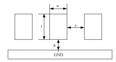
Fig. 1.
Two-plane interconnect structure.
SEMICONDUCTOR INTEGRATED CIRCUITS
Xiaoxian Liu, Zhangming Zhu, Yintang Yang, Fengjuan Wang and Ruixue Ding
Corresponding author: Zhu Zhangming, Email:zmyh@263.net
Abstract: In high speed three-dimensional integrated circuits (3D ICs), through silicon via (TSV) insertion causes impedance discontinuities along the interconnect-TSV channel that results in signal reflection. As demonstrated for a two-plane interconnect structure connected by a TSV, we incorporate an appropriate capacitance at the junction to mitigate the signal reflection with gigascale frequencies. Based on 65 nm technology and S-parameter analysis, the decrease of signal reflection can be 189% at the tuned frequency of 5 GHz. Extending this method to the five-plane interconnect structure further, the reduction of signal reflection can achieve 400%. So we could broaden this method to any multilevel 3D interconnect structures. This method can also be applied to a circuit with tunable operating frequencies by digitally connecting the corresponding matching capacitance into the circuit through switches. There are remarkable improvements of the quality of the transmitting signals.
Keywords: 3D integration, TSV, signal reflection, impedance matching, S-parameter
| [1] |
Pavlisis V F, Friedman E G. Three-dimensional integrated circuit design. San Mateo:Morgan Kaufmann, 2009
|
| [2] |
Savidis I, Friedman E G. Closed-form expressions of 3-D via resistance, inductance, and capacitance. IEEE Trans Electron Devices, 2009, 56(9):1873 doi: 10.1109/TED.2009.2026200
|
| [3] |
Zhu Z M, Qian L B, Yang Y T, et al. A novel interconnect-optimal repeater insertion model with a target delay constraint. Journal of Semiconductors, 2009, 29(9):1847 http://www.jos.ac.cn/bdtxbcn/ch/reader/view_abstract.aspx?file_no=09032303&flag=1
|
| [4] |
Zhu Z M, Qian L B, Yang Y T. A novel interconnect crosstalk parallel RLC analyzable model based on the 65 nm CMOS process. Journal of Semiconductors, 2008, 29(3):423 http://www.jos.ac.cn/bdtxbcn/ch/reader/view_abstract.aspx?file_no=07091601&flag=1
|
| [5] |
Yang Y T, Leng P, Dong G, et al. RLC interconnect delay with temperature distribution effects. Journal of Semiconductors, 2008, 29(9):1843 http://www.jos.ac.cn/bdtxbcn/ch/reader/view_abstract.aspx?file_no=07112202&flag=1
|
| [6] |
Chen J G, Hao Y Y, Chen Y H. A novel switched capacitor bandgap reference with a correlated double sampling structure. Journal of Semiconductors, 2013, 34(2):025009 doi: 10.1088/1674-4926/34/2/025009
|
| [7] |
Li J, Yang M, Sun W F, et al. A fast novel soft-start circuit for peak current-mode DC-DC buck converters. Journal of Semiconductors, 2013, 34(2):025006 doi: 10.1088/1674-4926/34/2/025006
|
| [8] |
Alam S M, Jones R E, Rauf D, et al. Inter-strata connection characteristics and signal transmission in three-dimensional (3D) integration technology. Quality Electronic Design, 2007:580 https://link.springer.com/content/pdf/bbm%3A978-1-4614-5508-0%2F1.pdf
|
| [9] |
Leung L L W, Chen K J. Microwave characterization and modeling of high aspect ratio through-wafer interconnect vias in silicon substrates. IEEE Trans Microw Theory Tech, 2005, 53(8):2472 doi: 10.1109/TMTT.2005.852782
|
| [10] |
Ryu C, Chung D, Lee J, et al. High frequency electrical circuit model of chip-to-chip vertical via interconnection for 3-D chip stacking package. Electrical Performance of Electronic Packaging, 2005:151 http://www.springer.com/cda/content/document/cda_downloaddocument/9789401790376-c2.pdf?SGWID=0-0-45-1458230-p176710300
|
| [11] |
Krishma S K, Bhat M S. Minimization of via-induced signal reflection in on-chip high speed interconnect lines. Circuits, Systems, and Signal Processing, 2012, 31(2):689 doi: 10.1007/s00034-011-9339-0
|
| [12] |
Qian L B, Zhu Z M, Yang Y T. Through-silicon-via insertion for performance optimization in three-dimensional integrated circuits. Microelectron J, 2012, 43(2):128 doi: 10.1016/j.mejo.2011.11.004
|
| [13] |
Liu E X, Lee H M, Wei X C, et al. Different designs of TSVs for 3D IC:signal integrity analysis with cascaded scattering matrix. Electrical Design of Advanced Packaging and Systems Symposium (EDAPS), 2011:12 http://ieeexplore.ieee.org/document/6213805/
|
| [14] |
Yew C W, Richard, Yak S K, et al. Comprehensive analysis of the impact of via design on high-speed signal integrity. Electronics Packaging Technology Conference, 2007:262
|
| [15] |
Hall S H, Hall G W, Call J A M. High-speed digital system design:a handbook of interconnect theory and design practices. New York:John Wiley& Sons, 2000
|
| [16] |
Predictive Technology Model (PTM). http://www.eas.asu.edu/ptm/
|
| [17] |
Katti G, Stucchi M, Meyer K D, et al. Electrical modeling and characterization of through silicon via for three-dimensional ICs. IEEE Trans Electron Devices, 2010, 57(1):256 doi: 10.1109/TED.2009.2034508
|
| [18] |
Xu C, Hong L. Compact AC modeling and performance analysis of through-silicon vias in 3-D ICs. IEEE Trans Electron Devices, 2010, 57(12):3045 http://www.jpier.org/PIERM/pierm42/06.15021404.pdf
|
| [19] |
Paul C R. Inductance:loop and partial. New York:John Wiley & Sons, 2010
|
| [20] |
Stephen H H, Howard L H. Advanced signal integrity for high-speed digital design. New York:John Wiley & Sons, 1985
|

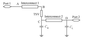
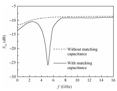
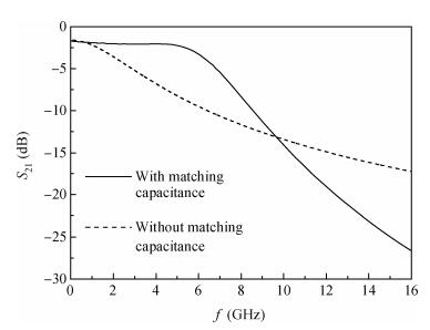
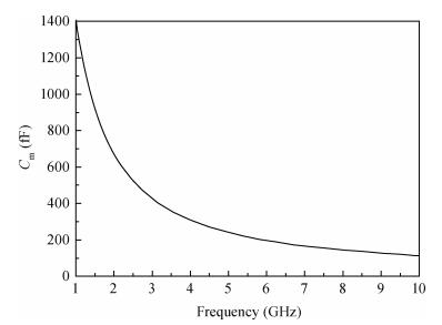
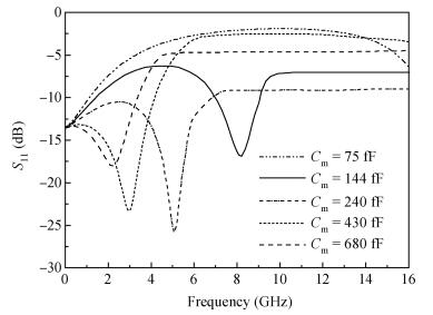
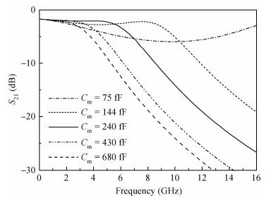

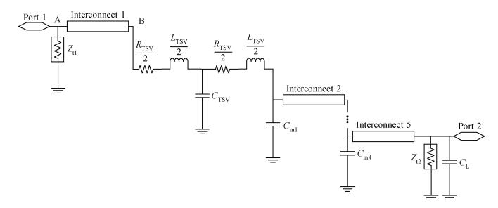
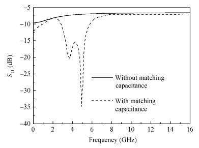
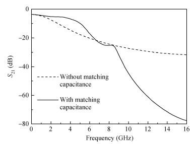
Table 1. Parameters of the interconnects.

|
Table 2. RLC parameters of Interconnect 1 and Interconnect 2.

|
Table 3. Design parameters of the TSV.

|
| [1] |
Pavlisis V F, Friedman E G. Three-dimensional integrated circuit design. San Mateo:Morgan Kaufmann, 2009
|
| [2] |
Savidis I, Friedman E G. Closed-form expressions of 3-D via resistance, inductance, and capacitance. IEEE Trans Electron Devices, 2009, 56(9):1873 doi: 10.1109/TED.2009.2026200
|
| [3] |
Zhu Z M, Qian L B, Yang Y T, et al. A novel interconnect-optimal repeater insertion model with a target delay constraint. Journal of Semiconductors, 2009, 29(9):1847 http://www.jos.ac.cn/bdtxbcn/ch/reader/view_abstract.aspx?file_no=09032303&flag=1
|
| [4] |
Zhu Z M, Qian L B, Yang Y T. A novel interconnect crosstalk parallel RLC analyzable model based on the 65 nm CMOS process. Journal of Semiconductors, 2008, 29(3):423 http://www.jos.ac.cn/bdtxbcn/ch/reader/view_abstract.aspx?file_no=07091601&flag=1
|
| [5] |
Yang Y T, Leng P, Dong G, et al. RLC interconnect delay with temperature distribution effects. Journal of Semiconductors, 2008, 29(9):1843 http://www.jos.ac.cn/bdtxbcn/ch/reader/view_abstract.aspx?file_no=07112202&flag=1
|
| [6] |
Chen J G, Hao Y Y, Chen Y H. A novel switched capacitor bandgap reference with a correlated double sampling structure. Journal of Semiconductors, 2013, 34(2):025009 doi: 10.1088/1674-4926/34/2/025009
|
| [7] |
Li J, Yang M, Sun W F, et al. A fast novel soft-start circuit for peak current-mode DC-DC buck converters. Journal of Semiconductors, 2013, 34(2):025006 doi: 10.1088/1674-4926/34/2/025006
|
| [8] |
Alam S M, Jones R E, Rauf D, et al. Inter-strata connection characteristics and signal transmission in three-dimensional (3D) integration technology. Quality Electronic Design, 2007:580 https://link.springer.com/content/pdf/bbm%3A978-1-4614-5508-0%2F1.pdf
|
| [9] |
Leung L L W, Chen K J. Microwave characterization and modeling of high aspect ratio through-wafer interconnect vias in silicon substrates. IEEE Trans Microw Theory Tech, 2005, 53(8):2472 doi: 10.1109/TMTT.2005.852782
|
| [10] |
Ryu C, Chung D, Lee J, et al. High frequency electrical circuit model of chip-to-chip vertical via interconnection for 3-D chip stacking package. Electrical Performance of Electronic Packaging, 2005:151 http://www.springer.com/cda/content/document/cda_downloaddocument/9789401790376-c2.pdf?SGWID=0-0-45-1458230-p176710300
|
| [11] |
Krishma S K, Bhat M S. Minimization of via-induced signal reflection in on-chip high speed interconnect lines. Circuits, Systems, and Signal Processing, 2012, 31(2):689 doi: 10.1007/s00034-011-9339-0
|
| [12] |
Qian L B, Zhu Z M, Yang Y T. Through-silicon-via insertion for performance optimization in three-dimensional integrated circuits. Microelectron J, 2012, 43(2):128 doi: 10.1016/j.mejo.2011.11.004
|
| [13] |
Liu E X, Lee H M, Wei X C, et al. Different designs of TSVs for 3D IC:signal integrity analysis with cascaded scattering matrix. Electrical Design of Advanced Packaging and Systems Symposium (EDAPS), 2011:12 http://ieeexplore.ieee.org/document/6213805/
|
| [14] |
Yew C W, Richard, Yak S K, et al. Comprehensive analysis of the impact of via design on high-speed signal integrity. Electronics Packaging Technology Conference, 2007:262
|
| [15] |
Hall S H, Hall G W, Call J A M. High-speed digital system design:a handbook of interconnect theory and design practices. New York:John Wiley& Sons, 2000
|
| [16] |
Predictive Technology Model (PTM). http://www.eas.asu.edu/ptm/
|
| [17] |
Katti G, Stucchi M, Meyer K D, et al. Electrical modeling and characterization of through silicon via for three-dimensional ICs. IEEE Trans Electron Devices, 2010, 57(1):256 doi: 10.1109/TED.2009.2034508
|
| [18] |
Xu C, Hong L. Compact AC modeling and performance analysis of through-silicon vias in 3-D ICs. IEEE Trans Electron Devices, 2010, 57(12):3045 http://www.jpier.org/PIERM/pierm42/06.15021404.pdf
|
| [19] |
Paul C R. Inductance:loop and partial. New York:John Wiley & Sons, 2010
|
| [20] |
Stephen H H, Howard L H. Advanced signal integrity for high-speed digital design. New York:John Wiley & Sons, 1985
|


Article views: 3387 Times PDF downloads: 33 Times Cited by: 0 Times
Received: 01 June 2013 Revised: 02 July 2013 Online: Published: 01 January 2014
| Citation: |
Xiaoxian Liu, Zhangming Zhu, Yintang Yang, Fengjuan Wang, Ruixue Ding. Impedance matching for the reduction of signal reflection in high speed multilevel three-dimensional integrated chips[J]. Journal of Semiconductors, 2014, 35(1): 015008. doi: 10.1088/1674-4926/35/1/015008
****
X X Liu, Z M Zhu, Y T Yang, F J Wang, R X Ding. Impedance matching for the reduction of signal reflection in high speed multilevel three-dimensional integrated chips[J]. J. Semicond., 2014, 35(1): 015008. doi: 10.1088/1674-4926/35/1/015008.

|
| [1] |
Pavlisis V F, Friedman E G. Three-dimensional integrated circuit design. San Mateo:Morgan Kaufmann, 2009
|
| [2] |
Savidis I, Friedman E G. Closed-form expressions of 3-D via resistance, inductance, and capacitance. IEEE Trans Electron Devices, 2009, 56(9):1873 doi: 10.1109/TED.2009.2026200
|
| [3] |
Zhu Z M, Qian L B, Yang Y T, et al. A novel interconnect-optimal repeater insertion model with a target delay constraint. Journal of Semiconductors, 2009, 29(9):1847 http://www.jos.ac.cn/bdtxbcn/ch/reader/view_abstract.aspx?file_no=09032303&flag=1
|
| [4] |
Zhu Z M, Qian L B, Yang Y T. A novel interconnect crosstalk parallel RLC analyzable model based on the 65 nm CMOS process. Journal of Semiconductors, 2008, 29(3):423 http://www.jos.ac.cn/bdtxbcn/ch/reader/view_abstract.aspx?file_no=07091601&flag=1
|
| [5] |
Yang Y T, Leng P, Dong G, et al. RLC interconnect delay with temperature distribution effects. Journal of Semiconductors, 2008, 29(9):1843 http://www.jos.ac.cn/bdtxbcn/ch/reader/view_abstract.aspx?file_no=07112202&flag=1
|
| [6] |
Chen J G, Hao Y Y, Chen Y H. A novel switched capacitor bandgap reference with a correlated double sampling structure. Journal of Semiconductors, 2013, 34(2):025009 doi: 10.1088/1674-4926/34/2/025009
|
| [7] |
Li J, Yang M, Sun W F, et al. A fast novel soft-start circuit for peak current-mode DC-DC buck converters. Journal of Semiconductors, 2013, 34(2):025006 doi: 10.1088/1674-4926/34/2/025006
|
| [8] |
Alam S M, Jones R E, Rauf D, et al. Inter-strata connection characteristics and signal transmission in three-dimensional (3D) integration technology. Quality Electronic Design, 2007:580 https://link.springer.com/content/pdf/bbm%3A978-1-4614-5508-0%2F1.pdf
|
| [9] |
Leung L L W, Chen K J. Microwave characterization and modeling of high aspect ratio through-wafer interconnect vias in silicon substrates. IEEE Trans Microw Theory Tech, 2005, 53(8):2472 doi: 10.1109/TMTT.2005.852782
|
| [10] |
Ryu C, Chung D, Lee J, et al. High frequency electrical circuit model of chip-to-chip vertical via interconnection for 3-D chip stacking package. Electrical Performance of Electronic Packaging, 2005:151 http://www.springer.com/cda/content/document/cda_downloaddocument/9789401790376-c2.pdf?SGWID=0-0-45-1458230-p176710300
|
| [11] |
Krishma S K, Bhat M S. Minimization of via-induced signal reflection in on-chip high speed interconnect lines. Circuits, Systems, and Signal Processing, 2012, 31(2):689 doi: 10.1007/s00034-011-9339-0
|
| [12] |
Qian L B, Zhu Z M, Yang Y T. Through-silicon-via insertion for performance optimization in three-dimensional integrated circuits. Microelectron J, 2012, 43(2):128 doi: 10.1016/j.mejo.2011.11.004
|
| [13] |
Liu E X, Lee H M, Wei X C, et al. Different designs of TSVs for 3D IC:signal integrity analysis with cascaded scattering matrix. Electrical Design of Advanced Packaging and Systems Symposium (EDAPS), 2011:12 http://ieeexplore.ieee.org/document/6213805/
|
| [14] |
Yew C W, Richard, Yak S K, et al. Comprehensive analysis of the impact of via design on high-speed signal integrity. Electronics Packaging Technology Conference, 2007:262
|
| [15] |
Hall S H, Hall G W, Call J A M. High-speed digital system design:a handbook of interconnect theory and design practices. New York:John Wiley& Sons, 2000
|
| [16] |
Predictive Technology Model (PTM). http://www.eas.asu.edu/ptm/
|
| [17] |
Katti G, Stucchi M, Meyer K D, et al. Electrical modeling and characterization of through silicon via for three-dimensional ICs. IEEE Trans Electron Devices, 2010, 57(1):256 doi: 10.1109/TED.2009.2034508
|
| [18] |
Xu C, Hong L. Compact AC modeling and performance analysis of through-silicon vias in 3-D ICs. IEEE Trans Electron Devices, 2010, 57(12):3045 http://www.jpier.org/PIERM/pierm42/06.15021404.pdf
|
| [19] |
Paul C R. Inductance:loop and partial. New York:John Wiley & Sons, 2010
|
| [20] |
Stephen H H, Howard L H. Advanced signal integrity for high-speed digital design. New York:John Wiley & Sons, 1985
|

 WeChat ID
Journal of Semiconductors © 2017 All Rights Reserved 京ICP备05085259号-2

 DownLoad: