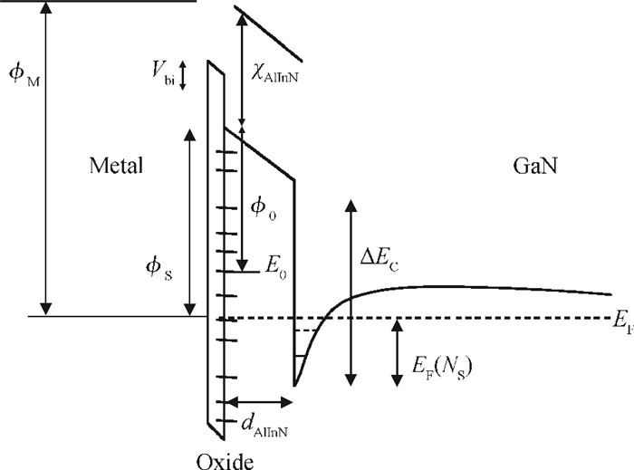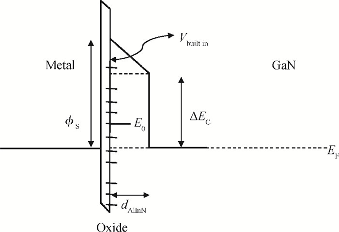
Fig. 1.
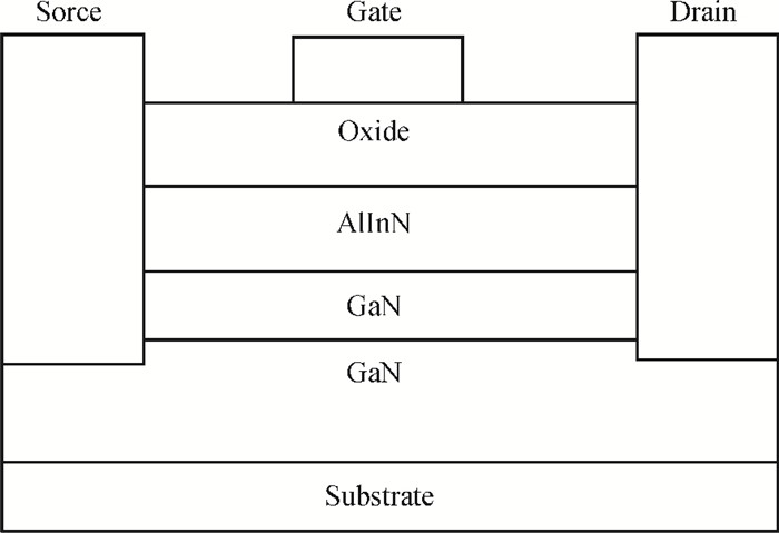
A MOSHEMT structure
SEMICONDUCTOR DEVICES
Devashish Pandey and T.R. Lenka
Corresponding author: T. R. Lenka, Email:trlenka@gmail.com
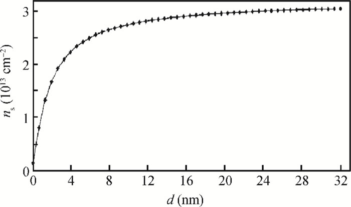
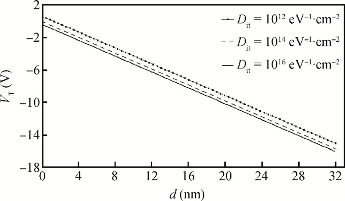
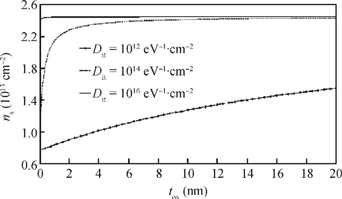
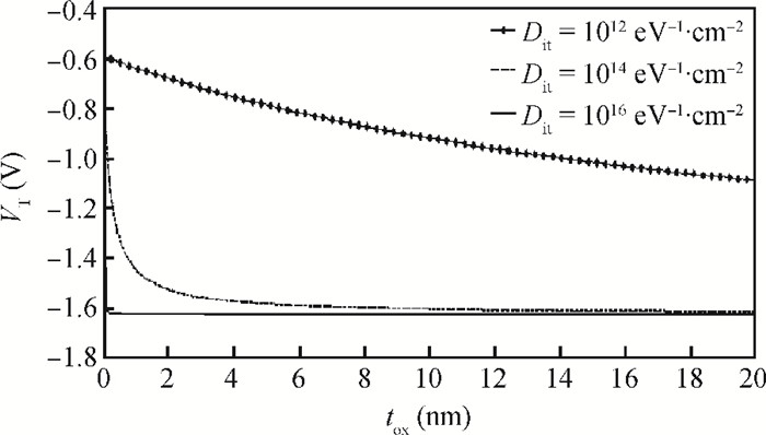
Abstract: A model predicting the behavior of various parameters, such as 2DEG sheet charge density and threshold voltage, with the variation of barrier thickness and oxide thickness considering interface density of states is presented. The mathematical dependence of these parameters is derived in conjunction with the interface density of states. The dependence of sheet charge density with the barrier thickness and with the oxide thickness is plotted and an insight into the barrier scaling properties of AlInN based MOSHEMTs is presented. The threshold voltage is also plotted with respect to barrier thickness and oxide thickness, which reveals the possibility of the enhancement mode operation of the device at low values of the interface DOS. The results are in good agreement with the fabricated device available in the literature.
Keywords: DOS, AlInN, MOSHEMT, 2DEG, barrier scaling
| [1] |
Maier D, Alomari M, Grandjean N, et al. InAlN/GaN HEMTs for operation in the 1000℃ regime:a first experiment. IEEE Electron Device Lett, 2012, 33(7):985 doi: 10.1109/LED.2012.2196972
|
| [2] |
Medjdoub F, Carlin J F, Gonschorek M, et al. Can InAlN/GaN be an alternative high power/high temperature AlGaN/GaN devices. Proc IEDM Tech Dig, 2006:1 https://infoscience.epfl.ch/record/210881?ln=en
|
| [3] |
Maier D, Alomari M, Grandjean N, et al. Testing the temperature limits of GaN-based devices. IEEE Trans Device Mater Rel, 2010, 10(4):427 doi: 10.1109/TDMR.2010.2072507
|
| [4] |
Chung J W, Saadat O I, Tirado J M, et al. Gate-recessed InAlN/GaN HEMTs on SiC substrate with Al2O3 passivation. IEEE Electron Device Lett, 2009, 30(9):904 doi: 10.1109/LED.2009.2026718
|
| [5] |
Vetury R, Zhang N Q, Keller S, et al. The impact of surface states on the DC and RF characteristics of AlGaN/GaN HFETs. IEEE Trans Electron Devices, 2001, 48(3):560 doi: 10.1109/16.906451
|
| [6] |
Bykhovski A D, Gelmont B L, Shur M S. Elastic strain relaxation and piezoeffect in GaN-AlN, GaN-AlGaN and GaN-InGaN superlattices. J Appl Phys, 1997, 81:6322 doi: 10.1063/1.364366
|
| [7] |
Kola S, Golio J M, Maracas G N. An analytical expression for Fermi level versus sheet carrier concentration for HEMT modeling. IEEE Electron Device Lett, 1988, 9(3):136 doi: 10.1109/55.2067
|
| [8] |
Li M, Wang Y. 2-D analytical model for current-voltage characteristics and transconductance of AlGaN/GaN MODFETs. IEEE Trans Electron Devices, 2008, 55(1):261 doi: 10.1109/TED.2007.911076
|
| [9] |
Cheng X W, Li M, Wang Y. Physics-based compact model for AlGaN/GaN MODFETs with close-formed I-V and C-V characteristics. IEEE Trans Electron Devices, 2009, 56(12):2881 doi: 10.1109/TED.2009.2030722
|
| [10] |
Medjdoub F, Alomari M, Carlin J F, et al. Barrier-layer scaling of InAlN/GaN HEMTs. IEEE Electron Device Lett, 2008, 29(5):422 doi: 10.1109/LED.2008.919377
|
| [11] |
Bhattacharjee A, Lenka T R. Performance analysis of 20 nm gate length In0.2Al0.8N/GaN HEMT with Cu-gate having a remarkable high ION/IOFF ratio. Journal of Semiconductors, 2014, 35(6):064002 doi: 10.1088/1674-4926/35/6/064002
|


Article views: 3895 Times PDF downloads: 40 Times Cited by: 0 Times
Received: 16 February 2014 Revised: Online: Published: 01 October 2014
| Citation: |
Devashish Pandey, T.R. Lenka. Model development for analyzing 2DEG sheet charge density and threshold voltage considering interface DOS for AlInN/GaN MOSHEMT[J]. Journal of Semiconductors, 2014, 35(10): 104001. doi: 10.1088/1674-4926/35/10/104001
****
D. Pandey, T.R. Lenka. Model development for analyzing 2DEG sheet charge density and threshold voltage considering interface DOS for AlInN/GaN MOSHEMT[J]. J. Semicond., 2014, 35(10): 104001. doi: 10.1088/1674-4926/35/10/104001.

|
| [1] |
Maier D, Alomari M, Grandjean N, et al. InAlN/GaN HEMTs for operation in the 1000℃ regime:a first experiment. IEEE Electron Device Lett, 2012, 33(7):985 doi: 10.1109/LED.2012.2196972
|
| [2] |
Medjdoub F, Carlin J F, Gonschorek M, et al. Can InAlN/GaN be an alternative high power/high temperature AlGaN/GaN devices. Proc IEDM Tech Dig, 2006:1 https://infoscience.epfl.ch/record/210881?ln=en
|
| [3] |
Maier D, Alomari M, Grandjean N, et al. Testing the temperature limits of GaN-based devices. IEEE Trans Device Mater Rel, 2010, 10(4):427 doi: 10.1109/TDMR.2010.2072507
|
| [4] |
Chung J W, Saadat O I, Tirado J M, et al. Gate-recessed InAlN/GaN HEMTs on SiC substrate with Al2O3 passivation. IEEE Electron Device Lett, 2009, 30(9):904 doi: 10.1109/LED.2009.2026718
|
| [5] |
Vetury R, Zhang N Q, Keller S, et al. The impact of surface states on the DC and RF characteristics of AlGaN/GaN HFETs. IEEE Trans Electron Devices, 2001, 48(3):560 doi: 10.1109/16.906451
|
| [6] |
Bykhovski A D, Gelmont B L, Shur M S. Elastic strain relaxation and piezoeffect in GaN-AlN, GaN-AlGaN and GaN-InGaN superlattices. J Appl Phys, 1997, 81:6322 doi: 10.1063/1.364366
|
| [7] |
Kola S, Golio J M, Maracas G N. An analytical expression for Fermi level versus sheet carrier concentration for HEMT modeling. IEEE Electron Device Lett, 1988, 9(3):136 doi: 10.1109/55.2067
|
| [8] |
Li M, Wang Y. 2-D analytical model for current-voltage characteristics and transconductance of AlGaN/GaN MODFETs. IEEE Trans Electron Devices, 2008, 55(1):261 doi: 10.1109/TED.2007.911076
|
| [9] |
Cheng X W, Li M, Wang Y. Physics-based compact model for AlGaN/GaN MODFETs with close-formed I-V and C-V characteristics. IEEE Trans Electron Devices, 2009, 56(12):2881 doi: 10.1109/TED.2009.2030722
|
| [10] |
Medjdoub F, Alomari M, Carlin J F, et al. Barrier-layer scaling of InAlN/GaN HEMTs. IEEE Electron Device Lett, 2008, 29(5):422 doi: 10.1109/LED.2008.919377
|
| [11] |
Bhattacharjee A, Lenka T R. Performance analysis of 20 nm gate length In0.2Al0.8N/GaN HEMT with Cu-gate having a remarkable high ION/IOFF ratio. Journal of Semiconductors, 2014, 35(6):064002 doi: 10.1088/1674-4926/35/6/064002
|

 WeChat ID
Journal of Semiconductors © 2017 All Rights Reserved 京ICP备05085259号-2

 DownLoad: