Processing math: 100%
J. Semicond. > 2014, Volume 35 > Issue 10 > 104003

SEMICONDUCTOR DEVICES

Self-heating and traps effects on the drain transient response of AlGaN/GaN HEMTs

Yamin Zhang, Shiwei Feng, Hui Zhu, Xueqin Gong, Bing Deng and Lin Ma

+ Author Affiliations

 Corresponding author: Feng Shiwei, Email:shwfeng@bjut.edu.cn

DOI: 10.1088/1674-4926/35/10/104003

PDF

Abstract: The effects of self-heating and traps on the drain current transient responses of AlGaN/GaN HEMTs are studied by 2D numerical simulation. The variation of the drain current simulated by the drain turn-on pulses has been analyzed. Our results show that temperature is the main factor for the drain current lag. The time that the drain current takes to reach a steady state depends on the thermal time constant, which is 80 μs in this case. The dynamics of the trapping of electron and channel electron density under drain turn-on pulse voltage are discussed in detail, which indicates that the accepter traps in the buffer are the major reason for the current collapse when the electric field significantly changes. The channel electron density has been shown to increase as the channel temperature rises.

Key words: AlGaN/GaN HEMTsdrain transient responsechannel temperature riseself-heatingtraps

AlGaN/GaN HEMTs have shown exceptional promise for high-frequency, high-voltage, and high-power applications[1, 2]. However, the high power dissipation of GaN-based HEMTs can result in substantial self-heating effects and parasitic effects induced by traps, which have detrimental effects on the electrical properties[3-5]. Drain current lag and collapse are major factors limiting these applications. It has been widely accepted that self-heating and traps are the two reasons for the drain current lag and collapse[6-9]. Information about the effect of traps and self-heating on the drain current transient response and the contribution of each factor is crucial for the optimization of the performance of AlGaN/GaN HEMTs.

The self-heating related thermal effects have been simulated by Turin et al.[10], Hu et al.[11] and Zhang et al.[12]. Meneghesso et al.[13] studied the trapping phenomena by changing the ambient temperature. The relationship between the channel temperature rise and drain current is not investigated in detail. Hu et al. [9] studied the thermal effects on drain current lag and current collapse by 2D numerical simulation. However, studies that include both the buffer trapping effects and the self-heating in the drain current transient response simulation are still lacking. Although Miccoli et al. [8] simulated the trapping effects and thermal effect on the drain transient response of AlGaN/GaN HEMTs, lattice heat flow simulation and electrical simulation are separated, their method only considered the process of heat conduction and did not consider electro-thermal coupling.

In this paper, we present the physical-based 2D numerical simulations of trapping and self-heating in the drain current transient response under drain turn-on pulse voltage. The intrinsic mechanisms of traps in GaN-buffer and self-heating effects on the drain current are investigated by trapped charge density evolution under the pulse-on drain bias. In addition, the contribution of traps in GaN-buffer and self-heating effects are analyzed through channel electron density.

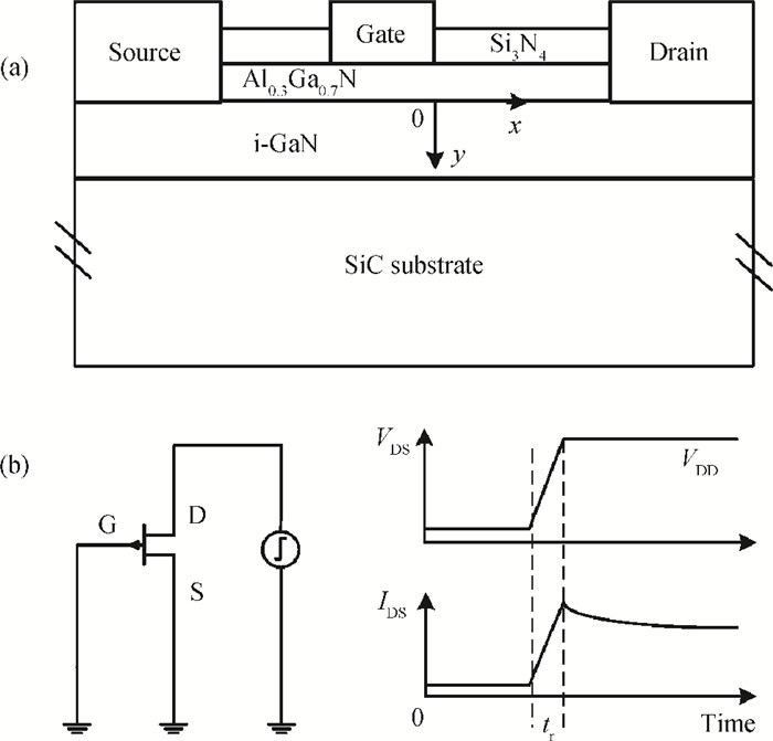
The schematic of the device structure for the simulation is given in Fig. 1(a). For the device, the thickness of intrinsic GaN and Al0.3Ga0.7N layer are of 2 μm and 25 nm, respectively. The gate length is 1.1 μm, and the spacing of gate-drain and gate-source are 2.4 μm and 1.5 μm, respectively. The thickness of SiC substrate is 100 μm. The ohmic contacts are used for the source and drain.

Figure  1.  The schematic of the device structure. (a) The structure parameters of device used for simulated. (b) The diagram of the circuit connection. It is used in simulations with a transient drain-source voltage to obtain the drain current response versus time.

The physical-based two-dimensional numerical simulation is performed by Sentaurus Device software, which is developed by Synopsys Inc. The thermodynamic model (also known as non-isothermal model) is applied to calculate the self-heating effect. The thermodynamic model is based on the drift-diffusion model and the effect of temperature gradient on the carrier transport is taken into account, which can be used to calibrate the uneven heat distribution from the self-heating effect. The equation of lattice heat flow is included, as are the basic Poisson equation and the continuity equation. The current of the device end and lattice temperature can be obtained from the self-consistent calculation of the above equations. Other related models are also used, such as the mobility model caused by surface scattering, field-dependent drift velocity model, the SRH (Shockley's-Read-Hall) composite model etc.

The traps of GaN buffer layer and AlGaN barrier layer are used in the simulation because they play an important role in charge transfer. The traps density of GaN is NGaN = 2.5 × 10¹⁶/cm3, with a capture cross section of σGaN = 1 × 10¹⁵/cm2. The traps density of GaN is NAlGaN = 1 × 10¹⁶/cm3, with a capture cross section of σGaN = 1 × 10¹⁵/cm2. The trap level is 1.0~eV below the conduction band. The interface charge induced by the polarization at AlGaN/GaN is included in our simulation as 1.2 × 10¹³/cm2. The calculation methods of polarization charge were described in Ref. [9, 10].

There exists a thermal boundary resistance between the GaN and the SiC [14] because the real interface between the epitaxial film and the growth substrate usually contains nucleation layers with a high density of defects and impurities. Here, we use a rather low thermal conductivity of 3.7 W/(Kcm) to effectively take account of the presence of thermal boundary resistance. The device usually has a top passivation layer with good thermal insulation, so that the heat dissipation from the top surface can be ignored. Such a choice of boundary condition has been validated by Turin et al.[10]. The thermal resistance of the electrode has been estimated by Wang et al.[15]. The heat transfer along the electrode can be ignored. Therefore, the heat is considered to diffuse only through the bottom of substrate.

The material parameters[8-10] for the simulation of transient temperature are listed in Table 1. Default values are used for other material parameters in the software.

Table  1.  The physical parameters of the material.
DownLoad: CSV  | Show Table

Mixed-mode simulations are selected because the device is operated under the pulse on mode. The diagram of the circuit connection is shown in Fig. 1(b). The drain is applied with a voltage source, which is pulsed from 0 V to VDD. The source and gate are grounded, and the DC voltage source is 0 V. A thermal electrode is attached to the bottom of the substrate, whose temperature and thermal resistance are set at a room temperature of 300 K and 1 × 10⁵ Kcm2/W in all simulations, respectively.

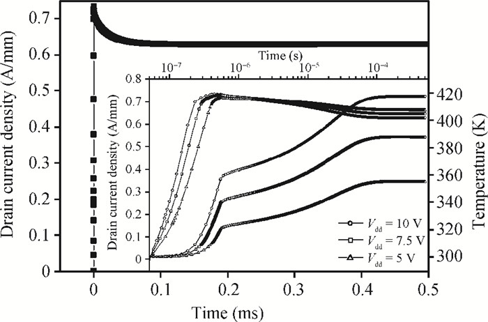
Figure 2 shows the simulated IDS(t) transients response to VDS turn-on pulse with VDD = 10 V. The simulated results show that IDS decreases exponentially [IDS(t) exp(t/τ)] with the characteristic time τ = 80 μs. IDS then decreases gradually to a steady-state with a collapse of about 12%. This result is similar to the experimental results and the theoretical models[5-9].

The drain current transient response of the AlGaN/GaN HEMTs device under different VDD is simulated to study the effect of self-heating on the drain current transient response, which is shown in the inset of Fig. 2. It is worth noting that the drain current does not continue to drop when the device channel temperature reaches a steady-state; that is, the time for the drain current to reach a steady state depends on the thermal time constant. Hence, the drain current transient response is affected by the channel temperature. The channel temperature increases as the drain voltage VDD increases. The electrical properties (such as, bandgap, electron mobility, etc.[3, 4, 16] are the function of channel temperature. Therefore, the drop of the drain current decreased, as is shown in the inset of Fig. 2.

Figure  2.  The simulated IDS(t) transients in response to VDS turn on pulse with VDD = 10 V. The inset show the IDS(t) and channel temperature transients in response to VDS turn-on pulse with VDD = 10, 7.5, 5 V, respectively.

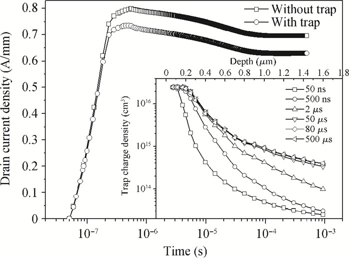
Besides the channel temperature, the drain current is also affected by the traps in the buffer. Figure 3 shows the simulation of IDS(t) transient in response to VDS turn on pulse, both with and without traps. The traps in the bulk have no effect on the variation trends of the transient drain current. It only impacts the magnitude of the drain current. This indicates that the acceptor traps in buffer are not a major reason for the drain lag.

Since the traps in buffer are under trapping and de-trapping, they will affect the channel electron density. For this reason, the trapped charge density and channel electron density at the drain side gate edge are calculated. The inset of Fig. 3 shows the spatial distributions of trapped charge density evolution under the pulse-on drain bias. It is can be seen that the thickness of fully filled by channel electrons increases when the drain voltage is pulsed from 0 to 10 V. The percentage of deep traps filled by electrons increases with time. The trapped charge density does not change in a time of t= 80 μs.

Figure  3.  Simulation of IDS(t) transient in response to VDS turn on pulse with and without traps. The inset shows that the spatial distributions of trapped charge density evolution under the pulse-on drain bias.

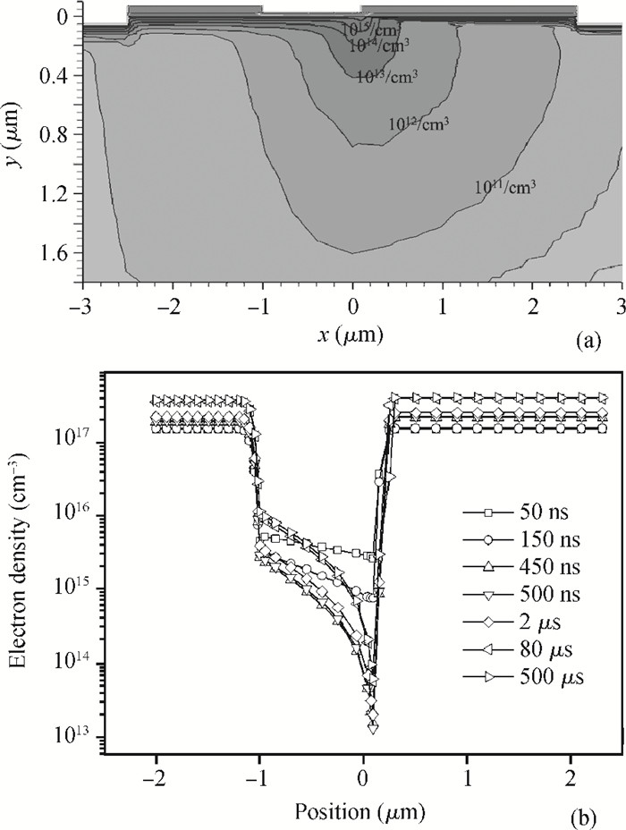
The injection of electrons from the channel into the buffer will lead to a change of the electron density in the channel. The GaN layer electron density distribution at 50 ns is shown in Fig. 4(a). The results for the evolution of channel electron density are shown in Fig. 4(b). A reduction in channel electron density is found as the drain bias pulsed from 0 to 10 V. It then increases to a steady state as the drain bias stays at 10 V. The difference between our simulation result and the results from drift--diffusion model is due to the involvement of lattice temperature.

Figure  4.  (a) The GaN buffer layer electron density distribution. (b) The channel electron density after VDD is applied.

There are two reasons for the filling of traps by electrons. One is that the channel electrons acquire enough energy when the electric field intensity increases. The hot electrons in the 2DEG channel generated under high drain bias could be injected into the adjacent epitaxial buffer layer, where they can be captured by donor like traps[16, 17]. The other reason is that the filled acceptor traps can emit electrons due to the increase of temperature and the 2DEG density increases as the temperature rises, which is the so called a de-trapping process[18]. In this case, the drain bias is pulsed from 0 to 10 V in 500 ns. The excess channel electrons can spill over in all directions under the drain bias and acquire enough energy. A number of electrons injects from the channel into the buffer at the gate edge and are captured by the traps. Although the temperature in the channel of device rises and the de-trapping exists, the trapping process is greater due to the change of electric field intensity. As the drain bias reaches a steady state, the electric field intensity will not change but the temperature of the channel rises rapidly[12]. The de-trapping process due to the increase of temperature becomes increasingly important until the trapping and de-trapping are in a dynamic equilibrium. The analysis is consistent with the experimental results, the 2DEG density increases as the temperature rises, which is studied by Maeda, et al.[18]. Therefore, the electron density of channel first decreases, and it then increases.

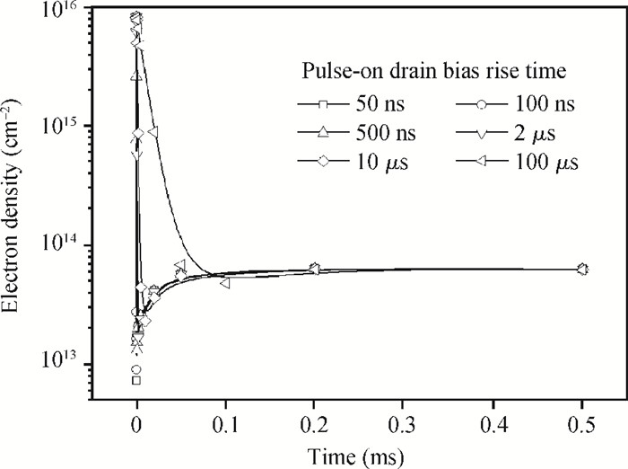
The evolution of channel electron density of the AlGaN/GaN HEMTs device under different rise time is simulated, as it is shown in Fig. 5. All of the results show a similar trend under different rising times, indicating that the electron density of channel decreases first and then increases. Moreover, the minimum of the channel electron density increases with the increase of rising time. This phenomenon is related to the effects of the electric field and temperature on the filling of traps by electrons.

Figure  5.  Channel electron density evolution in different rise times.

In summary, the effects of self-heating and traps on drain current of AlGaN/GaN HEMTs are studied by transient simulation. The simulated drain current transient response is in good agreement with both the reported experimental results and the theoretical models. The time of drain current reaching a steady state is dependent on the thermal time constant, which indicates that temperature is the main factor for the drain current lag because the electrical properties are affected by the channel temperature. The electron density of channel decreases first and then increases. This is related with the effects of electric field and temperature on the filling of traps by electrons.


[1]
Wang C, Chong C, He Y, et al. Breakdown voltage and current collapse of F-plasma treated AlGaN/GaN HEMTs. Journal of Semiconductors, 2014, 35(1):014008 doi: 10.1088/1674-4926/35/1/014008
[2]
Chu F, Chen C, Liu X. Breakdown voltage enhancement of AlGaN/GaN high electron mobility transistors by polyimide/chromium composite thin film passivation. Journal of Semiconductors, 2014, 35(3):034007 doi: 10.1088/1674-4926/35/3/034007
[3]
Yang Z, Wang J, Xu Z, et al. Analysis of AlGaN/GaN high electron mobility transistors failure mechanism under semi-on DC stress. Journal of Semiconductors, 2014, 35(1):014007 doi: 10.1088/1674-4926/35/1/014007
[4]
Zhang Y, Feng S, Zhu H, et al. Effect of self-heating on the drain current transient response in AlGaN/GaN HEMTs. IEEE Electron Device Lett, 2014, 35(3):345 doi: 10.1109/LED.2014.2300856
[5]
Tirado J M, Sánchez-Rojas J L, Izpura J I. Trapping effects in the transient response of AlGaN/GaN HEMT devices. IEEE Trans Electron Devices, 2007, 54(3):410 doi: 10.1109/TED.2006.890592
[6]
Wang X D, Hu W D, Chen X S, et al. The study of self-heating and hot-electron effects for AlGaN/GaN double-channel HEMTs. IEEE Trans Electron Devices, 2012, 59(5):1393 doi: 10.1109/TED.2012.2188634
[7]
Zhang W, Zhang Y, Mao W, et al. Influence of the interface acceptor-like traps on the transient response of AlGaN/GaN HEMTs. IEEE Electron Device Lett, 2013, 34(1):45 doi: 10.1109/LED.2012.2227235
[8]
Miccoli C, Martino V C, Reina S, et al. Trapping and thermal effects analysis for AlGaN/GaN HEMTs by means of TCAD simulations. IEEE Electron Device Lett, 2013, 34(9):1121 doi: 10.1109/LED.2013.2274326
[9]
Hu W D, Chen X S, Yin F, et al. Two-dimensional transient simulations of drain lag and current collapse in GaN-based high-electron-mobility transistors. J Appl Phys, 2009, 105(8):084502 doi: 10.1063/1.3106603
[10]
Turin V O, Balandin A A. Electrothermal simulation of the self-heating effects in GaN-based field-effect transistors. J Appl Phys, 2006, 100(5):054501 doi: 10.1063/1.2336299
[11]
Hu W D, Chen X S, Quan Z J, et al. Self-heating simulation of GaN-based metal-oxide-semiconductor high-electron-mobility transistors including hot electron and quantum effects. J Appl Phys, 2006, 100(7):074501 doi: 10.1063/1.2354327
[12]
Zhang Y, Feng S, Zhu H, et al. Two-dimensional transient simulations of the self-heating effects in GaN-based HEMTs. Microelectron Reliab, 2013, 53(5):694 doi: 10.1016/j.microrel.2013.02.004
[13]
Meneghesso G, Meneghini M, Bisi D, et al. Trapping phenomena in AlGaN/GaN HEMTs:a study based on pulsed and transient measurements. Semicond Sci Technol, 2013, 28(7):074021 doi: 10.1088/0268-1242/28/7/074021
[14]
Manoi A, Pomeroy J W, Killat N, et al. Benchmarking of thermal boundary resistance in AlGaN/GaN HEMTs on SiC substrates:implications of the nucleation layer microstructure. IEEE Electron Device Lett, 2010, 31(12):1395 doi: 10.1109/LED.2010.2077730
[15]
Wang L, Fjeldly T A, Iniguez B, et al. Self-heating and kink effects in a-Si:H thin film transistors. IEEE Trans Electron Devices, 2000, 47(2):387 doi: 10.1109/16.822285
[16]
Wang M, Chen K J. Kink effect in AlGaN/GaN HEMTs induced by drain and gate pumping. IEEE Electron Device Lett, 2011, 32(4):482 doi: 10.1109/LED.2011.2105460
[17]
Nakkala P, Martin A, Campovecchio M, et al. Pulsed characterisation of trapping dynamics in AlGaN/GaN HEMTs. Electron Lett, 2013, 49(22):1406 doi: 10.1049/el.2013.2304
[18]
Maeda N, Tsubaki K, Saitoh T, et al. High-temperature electron transport properties in AlGaN/GaN heterostructures. Appl Phys Lett, 2001, 79(11):1634 doi: 10.1063/1.1400779
Fig. 1.  The schematic of the device structure. (a) The structure parameters of device used for simulated. (b) The diagram of the circuit connection. It is used in simulations with a transient drain-source voltage to obtain the drain current response versus time.

Fig. 2.  The simulated IDS(t) transients in response to VDS turn on pulse with VDD = 10 V. The inset show the IDS(t) and channel temperature transients in response to VDS turn-on pulse with VDD = 10, 7.5, 5 V, respectively.

Fig. 3.  Simulation of IDS(t) transient in response to VDS turn on pulse with and without traps. The inset shows that the spatial distributions of trapped charge density evolution under the pulse-on drain bias.

Fig. 4.  (a) The GaN buffer layer electron density distribution. (b) The channel electron density after VDD is applied.

Fig. 5.  Channel electron density evolution in different rise times.

Table 1.   The physical parameters of the material.

[1]
Wang C, Chong C, He Y, et al. Breakdown voltage and current collapse of F-plasma treated AlGaN/GaN HEMTs. Journal of Semiconductors, 2014, 35(1):014008 doi: 10.1088/1674-4926/35/1/014008
[2]
Chu F, Chen C, Liu X. Breakdown voltage enhancement of AlGaN/GaN high electron mobility transistors by polyimide/chromium composite thin film passivation. Journal of Semiconductors, 2014, 35(3):034007 doi: 10.1088/1674-4926/35/3/034007
[3]
Yang Z, Wang J, Xu Z, et al. Analysis of AlGaN/GaN high electron mobility transistors failure mechanism under semi-on DC stress. Journal of Semiconductors, 2014, 35(1):014007 doi: 10.1088/1674-4926/35/1/014007
[4]
Zhang Y, Feng S, Zhu H, et al. Effect of self-heating on the drain current transient response in AlGaN/GaN HEMTs. IEEE Electron Device Lett, 2014, 35(3):345 doi: 10.1109/LED.2014.2300856
[5]
Tirado J M, Sánchez-Rojas J L, Izpura J I. Trapping effects in the transient response of AlGaN/GaN HEMT devices. IEEE Trans Electron Devices, 2007, 54(3):410 doi: 10.1109/TED.2006.890592
[6]
Wang X D, Hu W D, Chen X S, et al. The study of self-heating and hot-electron effects for AlGaN/GaN double-channel HEMTs. IEEE Trans Electron Devices, 2012, 59(5):1393 doi: 10.1109/TED.2012.2188634
[7]
Zhang W, Zhang Y, Mao W, et al. Influence of the interface acceptor-like traps on the transient response of AlGaN/GaN HEMTs. IEEE Electron Device Lett, 2013, 34(1):45 doi: 10.1109/LED.2012.2227235
[8]
Miccoli C, Martino V C, Reina S, et al. Trapping and thermal effects analysis for AlGaN/GaN HEMTs by means of TCAD simulations. IEEE Electron Device Lett, 2013, 34(9):1121 doi: 10.1109/LED.2013.2274326
[9]
Hu W D, Chen X S, Yin F, et al. Two-dimensional transient simulations of drain lag and current collapse in GaN-based high-electron-mobility transistors. J Appl Phys, 2009, 105(8):084502 doi: 10.1063/1.3106603
[10]
Turin V O, Balandin A A. Electrothermal simulation of the self-heating effects in GaN-based field-effect transistors. J Appl Phys, 2006, 100(5):054501 doi: 10.1063/1.2336299
[11]
Hu W D, Chen X S, Quan Z J, et al. Self-heating simulation of GaN-based metal-oxide-semiconductor high-electron-mobility transistors including hot electron and quantum effects. J Appl Phys, 2006, 100(7):074501 doi: 10.1063/1.2354327
[12]
Zhang Y, Feng S, Zhu H, et al. Two-dimensional transient simulations of the self-heating effects in GaN-based HEMTs. Microelectron Reliab, 2013, 53(5):694 doi: 10.1016/j.microrel.2013.02.004
[13]
Meneghesso G, Meneghini M, Bisi D, et al. Trapping phenomena in AlGaN/GaN HEMTs:a study based on pulsed and transient measurements. Semicond Sci Technol, 2013, 28(7):074021 doi: 10.1088/0268-1242/28/7/074021
[14]
Manoi A, Pomeroy J W, Killat N, et al. Benchmarking of thermal boundary resistance in AlGaN/GaN HEMTs on SiC substrates:implications of the nucleation layer microstructure. IEEE Electron Device Lett, 2010, 31(12):1395 doi: 10.1109/LED.2010.2077730
[15]
Wang L, Fjeldly T A, Iniguez B, et al. Self-heating and kink effects in a-Si:H thin film transistors. IEEE Trans Electron Devices, 2000, 47(2):387 doi: 10.1109/16.822285
[16]
Wang M, Chen K J. Kink effect in AlGaN/GaN HEMTs induced by drain and gate pumping. IEEE Electron Device Lett, 2011, 32(4):482 doi: 10.1109/LED.2011.2105460
[17]
Nakkala P, Martin A, Campovecchio M, et al. Pulsed characterisation of trapping dynamics in AlGaN/GaN HEMTs. Electron Lett, 2013, 49(22):1406 doi: 10.1049/el.2013.2304
[18]
Maeda N, Tsubaki K, Saitoh T, et al. High-temperature electron transport properties in AlGaN/GaN heterostructures. Appl Phys Lett, 2001, 79(11):1634 doi: 10.1063/1.1400779
1

Influence of self-heating on the millimeter-wave and terahertz performance of MBE grown silicon IMPATT diodes

S. J. Mukhopadhyay, Prajukta Mukherjee, Aritra Acharyya, Monojit Mitra

Journal of Semiconductors, 2020, 41(3): 032103. doi: 10.1088/1674-4926/41/3/032103

2

Investigation of current collapse and recovery time due to deep level defect traps in β-Ga2O3 HEMT

R. Singh, T. R. Lenka, R. T. Velpula, B. Jain, H. Q. T. Bui, et al.

Journal of Semiconductors, 2020, 41(10): 102802. doi: 10.1088/1674-4926/41/10/102802

3

Direct evidence of traps controlling the carriers transport in SnO2 nanobelts

Olivia M. Berengue, Adenilson J. Chiquito

Journal of Semiconductors, 2017, 38(12): 122001. doi: 10.1088/1674-4926/38/12/122001

4

A gate current 1/f noise model for GaN/AlGaN HEMTs

Yu'an Liu, Yiqi Zhuang

Journal of Semiconductors, 2014, 35(12): 124005. doi: 10.1088/1674-4926/35/12/124005

5

Effect of varying layouts on the gate temperature for multi-finger AlGaN/GaN HEMTs

Wang Jianhui, Wang Xinhua, Pang Lei, Chen Xiaojuan, Jin Zhi, et al.

Journal of Semiconductors, 2012, 33(9): 094004. doi: 10.1088/1674-4926/33/9/094004

6

Characterization of electrical properties of AlGaN/GaN interface using coupled Schrödinger and Poisson equation

S. Das, A. K. Panda, G. N. Dash

Journal of Semiconductors, 2012, 33(11): 113001. doi: 10.1088/1674-4926/33/11/113001

7

A Ku band internally matched high power GaN HEMT amplifier with over 30% of PAE

Ge Qin, Chen Xiaojuan, Luo Weijun, Yuan Tingting, Pu Yan, et al.

Journal of Semiconductors, 2012, 33(1): 014003. doi: 10.1088/1674-4926/33/1/014003

8

Extrinsic and intrinsic causes of the electrical degradation of AlGaN/GaN high electron mobility transistors

Fang Yulong, Dun Shaobo, Liu Bo, Yin Jiayun, Cai Shujun, et al.

Journal of Semiconductors, 2012, 33(5): 054005. doi: 10.1088/1674-4926/33/5/054005

9

A Ku-band high power density AlGaN/GaN HEMT monolithic power amplifier

Ge Qin, Chen Xiaojuan, Luo Weijun, Yuan Tingting, Pang Lei, et al.

Journal of Semiconductors, 2011, 32(8): 085001. doi: 10.1088/1674-4926/32/8/085001

10

High performance AlGaN/GaN HEMTs with 2.4 μm source–drain spacing

Wang Dongfang, Wei Ke, Yuan Tingting, Liu Xinyu

Journal of Semiconductors, 2010, 31(3): 034001. doi: 10.1088/1674-4926/31/3/034001

11

Finite element analysis of the temperature field in a vertical MOCVD reactor by induction heating

Li Zhiming, Xu Shengrui, Zhang Jincheng, Chang Yongming, Ni Jingyu, et al.

Journal of Semiconductors, 2009, 30(11): 113004. doi: 10.1088/1674-4926/30/11/113004

12

Annealing before gate metal deposition related noise performance in AlGaN/GaN HEMTs

Pang Lei, Pu Yan, Liu Xinyu, Wang Liang, Li Chengzhan, et al.

Journal of Semiconductors, 2009, 30(5): 054001. doi: 10.1088/1674-4926/30/5/054001

13

Noise performance in AlGaN/GaN HEMTs under high drain bias

Pang Lei, Pu Yan, Liu Xinyu, Wang Liang, Liu Jian, et al.

Journal of Semiconductors, 2009, 30(8): 084004. doi: 10.1088/1674-4926/30/8/084004

14

60Co γ-rays irradiation effect in DC performance of AlGaN/GaN high electron mobility transistors

Gu Wenping, Chen Chi, Duan Huantao, Hao Yue, Zhang Jincheng, et al.

Journal of Semiconductors, 2009, 30(4): 044002. doi: 10.1088/1674-4926/30/4/044002

15

Characterization and Reliability of Thin Film Resistors for MMICs Application Based on AlGaN/GaN HEMTs

Yao Xiaojiang, Pu Yan, Liu Xinyu, Wu Weichao

Journal of Semiconductors, 2008, 29(7): 1246-1248.

16

Development and Characteristic Analysis of MOS AlGaN/GaN HEMTs

Wang Chong, Yue Yuanzheng, Ma Xiaohua, Hao Yue, Feng Qian, et al.

Journal of Semiconductors, 2008, 29(8): 1557-1560.

17

An 8GHz Internally Matched AlGaN/GaN HEMT Power Amplifier with RC Stability Network

Zeng Xuan, Chen Xiaojuan, Liu Guoguo, Yuan Tingting, Chen Zhongzi, et al.

Journal of Semiconductors, 2008, 29(8): 1445-1448.

18

Performance Improvement of AlGaN/GaN HEMTs by Surface Treatment Prior to Si3N4 Passivation

Li Chengzhan, Liu Dan, Zheng Yingkui, Liu Xinyu, Liu Jian, et al.

Journal of Semiconductors, 2008, 29(2): 329-333.

19

Preparation and Properties of AlGaN/AIN/GaN HEMTs with Compositionally Step-Graded AIGaN Barrier Layer

Ma Zhiyong, Wang Xiaoliang, Hu Guoxin, Xiao Hongling, Wang Cuimei, et al.

Chinese Journal of Semiconductors , 2007, 28(S1): 3944-3943.

20

AlGaN/GaN HEMTs Power Amplifier MIC with Power Combining at C-Band

Yao Xiaojiang, Li Bin, Chen Yanhu, Chen Xiaojuan, Wei Ke, et al.

Chinese Journal of Semiconductors , 2007, 28(4): 514-517.

  • Search

    Advanced Search >>

    GET CITATION

    Yamin Zhang, Shiwei Feng, Hui Zhu, Xueqin Gong, Bing Deng, Lin Ma. Self-heating and traps effects on the drain transient response of AlGaN/GaN HEMTs[J]. Journal of Semiconductors, 2014, 35(10): 104003. doi: 10.1088/1674-4926/35/10/104003
    Y M Zhang, S W Feng, H Zhu, X Q Gong, B Deng, L Ma. Self-heating and traps effects on the drain transient response of AlGaN/GaN HEMTs[J]. J. Semicond., 2014, 35(10): 104003. doi: 10.1088/1674-4926/35/10/104003.
    shu

    Export: BibTex EndNote

    Article Metrics

    Article views: 2907 Times PDF downloads: 42 Times Cited by: 0 Times

    History

    Received: 26 February 2014 Revised: 16 April 2014 Online: Published: 01 October 2014

    Catalog

      Email This Article

      User name:
      Email:*请输入正确邮箱
      Code:*验证码错误
      Yamin Zhang, Shiwei Feng, Hui Zhu, Xueqin Gong, Bing Deng, Lin Ma. Self-heating and traps effects on the drain transient response of AlGaN/GaN HEMTs[J]. Journal of Semiconductors, 2014, 35(10): 104003. doi: 10.1088/1674-4926/35/10/104003 ****Y M Zhang, S W Feng, H Zhu, X Q Gong, B Deng, L Ma. Self-heating and traps effects on the drain transient response of AlGaN/GaN HEMTs[J]. J. Semicond., 2014, 35(10): 104003. doi: 10.1088/1674-4926/35/10/104003.
      Citation:
      Yamin Zhang, Shiwei Feng, Hui Zhu, Xueqin Gong, Bing Deng, Lin Ma. Self-heating and traps effects on the drain transient response of AlGaN/GaN HEMTs[J]. Journal of Semiconductors, 2014, 35(10): 104003. doi: 10.1088/1674-4926/35/10/104003 ****
      Y M Zhang, S W Feng, H Zhu, X Q Gong, B Deng, L Ma. Self-heating and traps effects on the drain transient response of AlGaN/GaN HEMTs[J]. J. Semicond., 2014, 35(10): 104003. doi: 10.1088/1674-4926/35/10/104003.

      Self-heating and traps effects on the drain transient response of AlGaN/GaN HEMTs

      DOI: 10.1088/1674-4926/35/10/104003
      Funds:

      Doctoral Fund of Innovation of Beijing University of Technology 

      Guangdong Strategic Emerging Industry Project of China 2012A080304003

      Beijing Natural Science Foundation 4132022

      Beijing Natural Science Foundation 4122005

      Project supported by the National Natural Science Foundation of China (Nos.61376077, 61201046, 61204081), the Beijing Natural Science Foundation (Nos.4132022, 4122005), the Guangdong Strategic Emerging Industry Project of China (No.2012A080304003), and the Doctoral Fund of Innovation of Beijing University of Technology

      Project supported by the National Natural Science Foundation of China 61376077

      Project supported by the National Natural Science Foundation of China 61204081

      Project supported by the National Natural Science Foundation of China 61201046

      More Information
      • Corresponding author: Feng Shiwei, Email:shwfeng@bjut.edu.cn
      • Received Date: 2014-02-26
      • Revised Date: 2014-04-16
      • Published Date: 2014-10-01

      Catalog

        /

        DownLoad:  Full-Size Img  PowerPoint
        Return
        Return