Fig. 1.
Three-dimensional view of double super junction (DSJ) LDMOS.
SEMICONDUCTOR DEVICES
Hui Zhu1, Haiou Li1, , Qi Li1, 2, Yuanhao Huang1, Xiaoning Xu1 and Hailiang Zhao1
Corresponding author: Li Haiou, Email:290557482@qq.com
Abstract: A novel multiple super junction (MSJ) LDMOS power device is proposed to decrease Ron due to lateral and vertical interactions between the N-pillar and P-pillar. In the studied device:multiple layers of SJ are introduced oppositely under surface SJ; when compared with 2D-depleting of the conventional super junction (CSJ), a 3D-depleted effect is formed in the MSJ thanks to vertical electric field modulation; and, current distribution is improved by deep drain, which increases the drift doping concentration and results in a lower on-resistance. The high electric field around the drain region by substrate-assisted depleted effect is reduced due to the charge balance result from the electric field shielding effect of the bottom SJ, which causes the uniform electric field in the drift region and the high breakdown voltage. The numerical simulation results indicate that the specific on-resistance of the MSJ device is reduced by 42% compared with that of CSJ device, while maintaining a high breakdown voltage; the cell pitch of the device is 12 μm.
Keywords: multiple super junction, 3D-depleted, breakdown voltage, specific on-resistance, electric field shielding effect
| [1] |
Rub M, Bar M, Deml G, et al. A 600 V 8.7 Ohmmm2 lateral superjunction transistor. Proc ISPSD, 2006:1 http://ieeexplore.ieee.org/document/1666132/keywords
|
| [2] |
Nassif-Khalil S G, Salama C A T. Super-junction LDMOS on a silicon-on-sapphire substrate. IEEE Trans Electron Devices, 2003, 50(5):1385 doi: 10.1109/TED.2003.813460
|
| [3] |
Park I Y, Salama C A T. New super-junction LDMOS with N-buffer layer. IEEE Trans Electron Devices, 2006, 53(8):1909 doi: 10.1109/TED.2006.877007
|
| [4] |
Chen W J, Zhang B, Li Z J. Realizing high breakdown voltage SJ-LDMOS on bulk silicon using a partial n-buried layer. Chinese Journal of Semiconductors, 2007, 28(3):355 http://en.cnki.com.cn/Article_en/CJFDTOTAL-BDTX200703008.htm
|
| [5] |
Wu W, Zhang B, Fang J, et al. High-voltage super-junction lateral double-diffused metal oxide semiconductor with a partial lightly doped pillar. Chin Phys B, 2013, 22(6):637.
|
| [6] |
Zhang B, Wang W L, Chen W J, et al. High-voltage LDMOS with charge-balanced surface low on-resistance path layer. IEEE Electron Device Lett, 200930(8):849 doi: 10.1109/LED.2009.2023541
|
| [7] |
Kanechika M, Kodama M, Uesugi T, et al. A concept of SOI RESURF lateral devices with striped trench electrodes. IEEE Trans Electron Devices, 2005, 52(6):1205 doi: 10.1109/TED.2005.848093
|
| [8] |
Onishi Y, Wang H, Xu H P E, et al. SJ-FINFET:a new low voltage lateral superjunction MOSFET. Proc ISPSD, 2008:111 http://ieeexplore.ieee.org/document/4538910/keywords
|
| [9] |
Duan B X, Zhang B, Li Z J. New lateral super junction MOSFETs with n+-floating layer on high-resistance substrate. Chinese Journal of Semiconductors, 2007, 28(2):166 http://ieeexplore.ieee.org/document/4538910/keywords
|
| [10] |
Permthammasin K, Wachutka G, Schmitt M, et al. New 600V lateral superjunction power MOSEFTs based on embedded non-uniform column structure. Proc ASDAM, 2006:263 doi: 10.1088/1674-4926/35/10/104006/meta
|

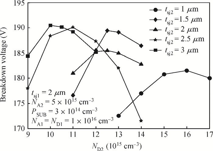
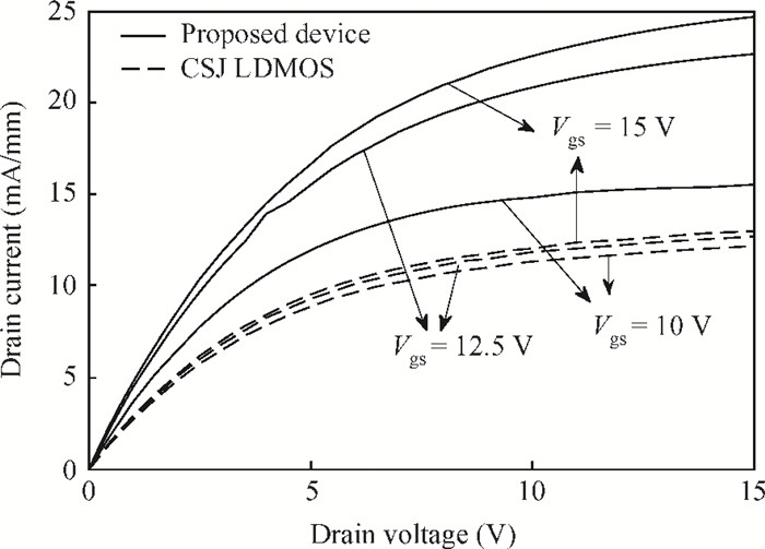
Table 1. Parameters used in the simulation

|
Table 2. Optimal results for proposed structure and other device.

|
| [1] |
Rub M, Bar M, Deml G, et al. A 600 V 8.7 Ohmmm2 lateral superjunction transistor. Proc ISPSD, 2006:1 http://ieeexplore.ieee.org/document/1666132/keywords
|
| [2] |
Nassif-Khalil S G, Salama C A T. Super-junction LDMOS on a silicon-on-sapphire substrate. IEEE Trans Electron Devices, 2003, 50(5):1385 doi: 10.1109/TED.2003.813460
|
| [3] |
Park I Y, Salama C A T. New super-junction LDMOS with N-buffer layer. IEEE Trans Electron Devices, 2006, 53(8):1909 doi: 10.1109/TED.2006.877007
|
| [4] |
Chen W J, Zhang B, Li Z J. Realizing high breakdown voltage SJ-LDMOS on bulk silicon using a partial n-buried layer. Chinese Journal of Semiconductors, 2007, 28(3):355 http://en.cnki.com.cn/Article_en/CJFDTOTAL-BDTX200703008.htm
|
| [5] |
Wu W, Zhang B, Fang J, et al. High-voltage super-junction lateral double-diffused metal oxide semiconductor with a partial lightly doped pillar. Chin Phys B, 2013, 22(6):637.
|
| [6] |
Zhang B, Wang W L, Chen W J, et al. High-voltage LDMOS with charge-balanced surface low on-resistance path layer. IEEE Electron Device Lett, 200930(8):849 doi: 10.1109/LED.2009.2023541
|
| [7] |
Kanechika M, Kodama M, Uesugi T, et al. A concept of SOI RESURF lateral devices with striped trench electrodes. IEEE Trans Electron Devices, 2005, 52(6):1205 doi: 10.1109/TED.2005.848093
|
| [8] |
Onishi Y, Wang H, Xu H P E, et al. SJ-FINFET:a new low voltage lateral superjunction MOSFET. Proc ISPSD, 2008:111 http://ieeexplore.ieee.org/document/4538910/keywords
|
| [9] |
Duan B X, Zhang B, Li Z J. New lateral super junction MOSFETs with n+-floating layer on high-resistance substrate. Chinese Journal of Semiconductors, 2007, 28(2):166 http://ieeexplore.ieee.org/document/4538910/keywords
|
| [10] |
Permthammasin K, Wachutka G, Schmitt M, et al. New 600V lateral superjunction power MOSEFTs based on embedded non-uniform column structure. Proc ASDAM, 2006:263 doi: 10.1088/1674-4926/35/10/104006/meta
|


Article views: 4608 Times PDF downloads: 36 Times Cited by: 0 Times
Received: 12 March 2014 Revised: 27 April 2014 Online: Published: 01 October 2014
| Citation: |
Hui Zhu, Haiou Li, Qi Li, Yuanhao Huang, Xiaoning Xu, Hailiang Zhao. A novel multiple super junction power device structure with low specific on-resistance[J]. Journal of Semiconductors, 2014, 35(10): 104006. doi: 10.1088/1674-4926/35/10/104006
****
H Zhu, H O Li, Q Li, Y H Huang, X N Xu, H L Zhao. A novel multiple super junction power device structure with low specific on-resistance[J]. J. Semicond., 2014, 35(10): 104006. doi: 10.1088/1674-4926/35/10/104006.

|
| [1] |
Rub M, Bar M, Deml G, et al. A 600 V 8.7 Ohmmm2 lateral superjunction transistor. Proc ISPSD, 2006:1 http://ieeexplore.ieee.org/document/1666132/keywords
|
| [2] |
Nassif-Khalil S G, Salama C A T. Super-junction LDMOS on a silicon-on-sapphire substrate. IEEE Trans Electron Devices, 2003, 50(5):1385 doi: 10.1109/TED.2003.813460
|
| [3] |
Park I Y, Salama C A T. New super-junction LDMOS with N-buffer layer. IEEE Trans Electron Devices, 2006, 53(8):1909 doi: 10.1109/TED.2006.877007
|
| [4] |
Chen W J, Zhang B, Li Z J. Realizing high breakdown voltage SJ-LDMOS on bulk silicon using a partial n-buried layer. Chinese Journal of Semiconductors, 2007, 28(3):355 http://en.cnki.com.cn/Article_en/CJFDTOTAL-BDTX200703008.htm
|
| [5] |
Wu W, Zhang B, Fang J, et al. High-voltage super-junction lateral double-diffused metal oxide semiconductor with a partial lightly doped pillar. Chin Phys B, 2013, 22(6):637.
|
| [6] |
Zhang B, Wang W L, Chen W J, et al. High-voltage LDMOS with charge-balanced surface low on-resistance path layer. IEEE Electron Device Lett, 200930(8):849 doi: 10.1109/LED.2009.2023541
|
| [7] |
Kanechika M, Kodama M, Uesugi T, et al. A concept of SOI RESURF lateral devices with striped trench electrodes. IEEE Trans Electron Devices, 2005, 52(6):1205 doi: 10.1109/TED.2005.848093
|
| [8] |
Onishi Y, Wang H, Xu H P E, et al. SJ-FINFET:a new low voltage lateral superjunction MOSFET. Proc ISPSD, 2008:111 http://ieeexplore.ieee.org/document/4538910/keywords
|
| [9] |
Duan B X, Zhang B, Li Z J. New lateral super junction MOSFETs with n+-floating layer on high-resistance substrate. Chinese Journal of Semiconductors, 2007, 28(2):166 http://ieeexplore.ieee.org/document/4538910/keywords
|
| [10] |
Permthammasin K, Wachutka G, Schmitt M, et al. New 600V lateral superjunction power MOSEFTs based on embedded non-uniform column structure. Proc ASDAM, 2006:263 doi: 10.1088/1674-4926/35/10/104006/meta
|

 WeChat ID
Journal of Semiconductors © 2017 All Rights Reserved 京ICP备05085259号-2

 DownLoad: