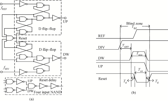
Fig. 1.
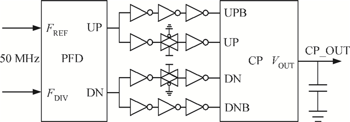
(a) Gate level implementation of the proposed PFD. (b) Diagram of blind zone production.
SEMICONDUCTOR INTEGRATED CIRCUITS
Faen Liu, Zhigong Wang, Zhiqun Li, Qin Li and Sheng Chen
Corresponding author: Liu Faen,Email:liufaenseu@gmail.com; Wang Zhigong,Email:zgwang@seu.edu.cn
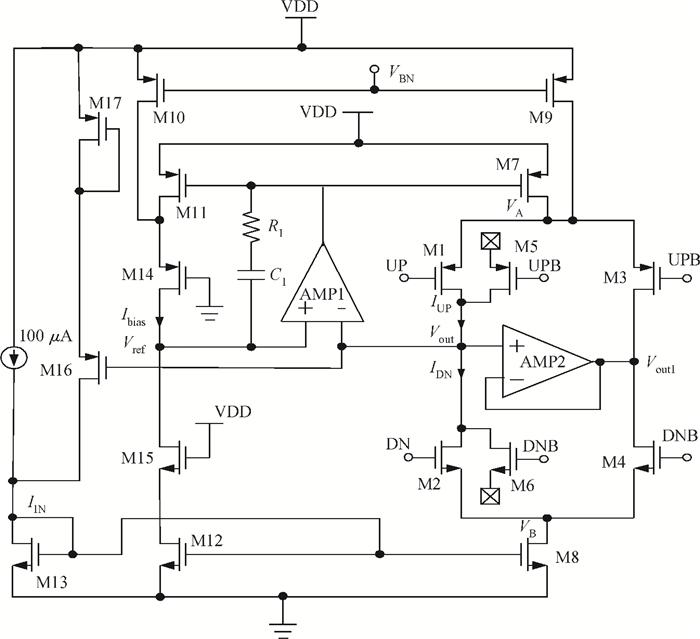
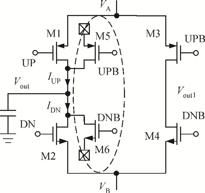
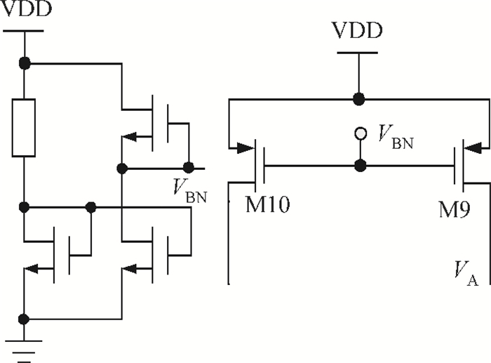
Abstract: Two essential blocks for the PLLs based on CP, a phase-frequency detector (PFD) and an improved current steering charge-pump (CP), are developed. The mechanisms for widening the phase error detection range and eliminating the dead zone are analyzed and applied in our design to optimize the proposed PFD. To obtain excellent current matching and minimum current variation over a wide output voltage range, an improved structure for the proposed CP is developed by fully utilizing many additional sub-circuits. Implemented in a standard 90-nm CMOS process, the proposed PFD achieves a phase error detection range from -354 ° to 354 ° and the improved CP demonstrates a current mismatch of less than 1.1% and a pump-current variation of 4% across the output voltage, swinging from 0.2 to 1.1 V, and the power consumption is 1.3 mW under a 1.2-V supply.
Keywords: CMOS, phase-frequency detector, charge-pump, current compensation, accelerating acquisition, PLL
| [1] |
Lee J Y, Lee S H, Haecheon K, et al. 28.5-32-GHz fast settling multichannel PLL synthesizer for 60-GHz WPAN radio. IEEE Microwave Theory Tech, 2008, 56(5):1234 doi: 10.1109/TMTT.2008.920179
|
| [2] |
Kailuke A C, Agrawal P, Kshirsagar R V. Design of phase frequency detector and charge pump for low voltage high frequency PLL. Electronic Systems, Signal Processing and Computing Technologies, 2014:74 http://ieeexplore.ieee.org/abstract/document/6745349/
|
| [3] |
Anush K N K, Mangalam H, Dharani V A, et al. Comparison and analysis of various PFD architecture for a phase locked loop design. Computational Intelligence and Computing Research (ICCIC), 2013:1 http://ieeexplore.ieee.org/document/6724238/
|
| [4] |
Chen W H, Inerowicz M E, Jung B. Phase frequency detector with minimal blind zone for fast frequency acquisition. IEEE Trans Circuits Syst Ⅱ:Express Briefs, 2010, 57(12):936 doi: 10.1109/TCSII.2010.2087951
|
| [5] |
Han S Y, Jin J, Mao C. A full-swing charge pump with zero phase offset. Microelectron Electron, 2009:298 http://ieeexplore.ieee.org/document/5397388/authors
|
| [6] |
Liu P, Sun P, Jung J, et al. PLL charge pump with adaptive body-bias compensation for minimum current variation. Electron Lett, 2012, 48(1):16 doi: 10.1049/el.2011.2835
|
| [7] |
Feng S, Tong H T, Silva-Martinez J, et al. Design and analysis of an ultra-speed glitch-free fully differential charge pump with minimum output current variation and accurate matching. IEEE Trans Circuits Syst Ⅱ:Express Briefs, 2006, 53(9):843 doi: 10.1109/TCSII.2006.879100
|
| [8] |
Hwang M S, Kim J, Jeong D K. Reduction of pump current mismatch in charge-pump PLL. Electron Lett, 2009, 45(3):135 doi: 10.1049/el:20092727
|
| [9] |
Zheng S S, Li Z Q. A novel CMOS charge pump with high performance for phase-locked loops synthesizer. IEEE Commun Technol, 2011:1062 http://ieeexplore.ieee.org/document/6158043/?reload=true&arnumber=6158043&punumber%3D6153171]
|
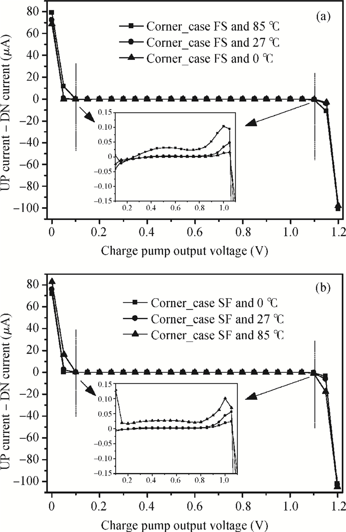
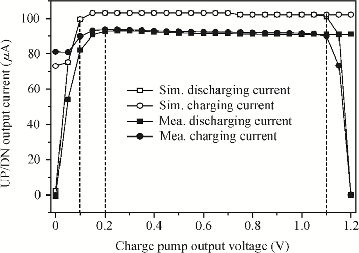
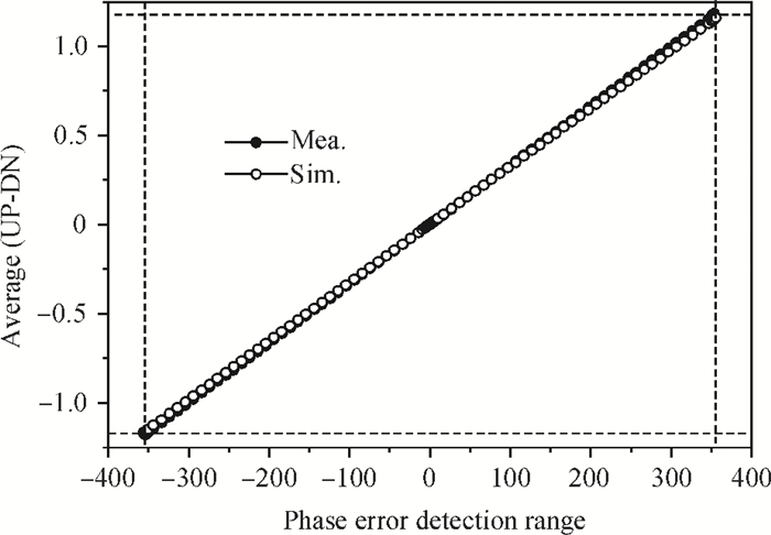
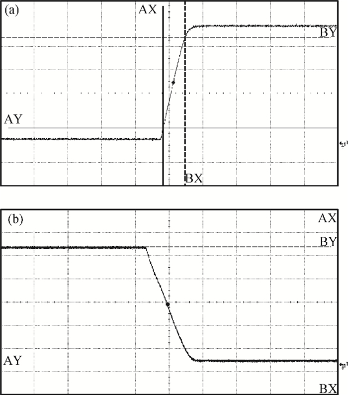
Table 1. Comparison of the performances for the currently published CPs.

|
| [1] |
Lee J Y, Lee S H, Haecheon K, et al. 28.5-32-GHz fast settling multichannel PLL synthesizer for 60-GHz WPAN radio. IEEE Microwave Theory Tech, 2008, 56(5):1234 doi: 10.1109/TMTT.2008.920179
|
| [2] |
Kailuke A C, Agrawal P, Kshirsagar R V. Design of phase frequency detector and charge pump for low voltage high frequency PLL. Electronic Systems, Signal Processing and Computing Technologies, 2014:74 http://ieeexplore.ieee.org/abstract/document/6745349/
|
| [3] |
Anush K N K, Mangalam H, Dharani V A, et al. Comparison and analysis of various PFD architecture for a phase locked loop design. Computational Intelligence and Computing Research (ICCIC), 2013:1 http://ieeexplore.ieee.org/document/6724238/
|
| [4] |
Chen W H, Inerowicz M E, Jung B. Phase frequency detector with minimal blind zone for fast frequency acquisition. IEEE Trans Circuits Syst Ⅱ:Express Briefs, 2010, 57(12):936 doi: 10.1109/TCSII.2010.2087951
|
| [5] |
Han S Y, Jin J, Mao C. A full-swing charge pump with zero phase offset. Microelectron Electron, 2009:298 http://ieeexplore.ieee.org/document/5397388/authors
|
| [6] |
Liu P, Sun P, Jung J, et al. PLL charge pump with adaptive body-bias compensation for minimum current variation. Electron Lett, 2012, 48(1):16 doi: 10.1049/el.2011.2835
|
| [7] |
Feng S, Tong H T, Silva-Martinez J, et al. Design and analysis of an ultra-speed glitch-free fully differential charge pump with minimum output current variation and accurate matching. IEEE Trans Circuits Syst Ⅱ:Express Briefs, 2006, 53(9):843 doi: 10.1109/TCSII.2006.879100
|
| [8] |
Hwang M S, Kim J, Jeong D K. Reduction of pump current mismatch in charge-pump PLL. Electron Lett, 2009, 45(3):135 doi: 10.1049/el:20092727
|
| [9] |
Zheng S S, Li Z Q. A novel CMOS charge pump with high performance for phase-locked loops synthesizer. IEEE Commun Technol, 2011:1062 http://ieeexplore.ieee.org/document/6158043/?reload=true&arnumber=6158043&punumber%3D6153171]
|


Article views: 5824 Times PDF downloads: 353 Times Cited by: 0 Times
Received: 20 March 2014 Revised: 08 May 2014 Online: Published: 01 October 2014
| Citation: |
Faen Liu, Zhigong Wang, Zhiqun Li, Qin Li, Sheng Chen. Design of improved CMOS phase-frequency detector and charge-pump for phase-locked loop[J]. Journal of Semiconductors, 2014, 35(10): 105006. doi: 10.1088/1674-4926/35/10/105006
****
F E Liu, Z G Wang, Z Q Li, Q Li, S Chen. Design of improved CMOS phase-frequency detector and charge-pump for phase-locked loop[J]. J. Semicond., 2014, 35(10): 105006. doi: 10.1088/1674-4926/35/10/105006.

|
| [1] |
Lee J Y, Lee S H, Haecheon K, et al. 28.5-32-GHz fast settling multichannel PLL synthesizer for 60-GHz WPAN radio. IEEE Microwave Theory Tech, 2008, 56(5):1234 doi: 10.1109/TMTT.2008.920179
|
| [2] |
Kailuke A C, Agrawal P, Kshirsagar R V. Design of phase frequency detector and charge pump for low voltage high frequency PLL. Electronic Systems, Signal Processing and Computing Technologies, 2014:74 http://ieeexplore.ieee.org/abstract/document/6745349/
|
| [3] |
Anush K N K, Mangalam H, Dharani V A, et al. Comparison and analysis of various PFD architecture for a phase locked loop design. Computational Intelligence and Computing Research (ICCIC), 2013:1 http://ieeexplore.ieee.org/document/6724238/
|
| [4] |
Chen W H, Inerowicz M E, Jung B. Phase frequency detector with minimal blind zone for fast frequency acquisition. IEEE Trans Circuits Syst Ⅱ:Express Briefs, 2010, 57(12):936 doi: 10.1109/TCSII.2010.2087951
|
| [5] |
Han S Y, Jin J, Mao C. A full-swing charge pump with zero phase offset. Microelectron Electron, 2009:298 http://ieeexplore.ieee.org/document/5397388/authors
|
| [6] |
Liu P, Sun P, Jung J, et al. PLL charge pump with adaptive body-bias compensation for minimum current variation. Electron Lett, 2012, 48(1):16 doi: 10.1049/el.2011.2835
|
| [7] |
Feng S, Tong H T, Silva-Martinez J, et al. Design and analysis of an ultra-speed glitch-free fully differential charge pump with minimum output current variation and accurate matching. IEEE Trans Circuits Syst Ⅱ:Express Briefs, 2006, 53(9):843 doi: 10.1109/TCSII.2006.879100
|
| [8] |
Hwang M S, Kim J, Jeong D K. Reduction of pump current mismatch in charge-pump PLL. Electron Lett, 2009, 45(3):135 doi: 10.1049/el:20092727
|
| [9] |
Zheng S S, Li Z Q. A novel CMOS charge pump with high performance for phase-locked loops synthesizer. IEEE Commun Technol, 2011:1062 http://ieeexplore.ieee.org/document/6158043/?reload=true&arnumber=6158043&punumber%3D6153171]
|

 WeChat ID
Journal of Semiconductors © 2017 All Rights Reserved 京ICP备05085259号-2

 DownLoad: