


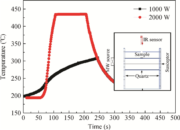
Fig. 1.
Plot of sample annealing temperature as a function of time for different powers. Inset: schematic of the MWA equipment.
SEMICONDUCTOR PHYSICS
Shirui Zhao, Yabin Dong, Mingyan Yu, Xiaolong Guo, Xinwei Xu, Yupeng Jing and Yang Xia
Corresponding author: Jing Yupeng, Email:jingyupeng@ime.ac.cn
Abstract: Zinc oxide thin films deposited on glass substrate at 150℃ by atomic layer deposition were annealed by the microwave method at temperatures below 500℃. The microwave annealing effects on the structural and luminescent properties of ZnO films have been investigated by X-ray diffraction and photoluminescence. The results show that the MWA process can increase the crystal quality of ZnO thin films with a lower annealing temperature than RTA and relatively decrease the green luminescence of ZnO films. The observed changes have demonstrated that MWA is a viable technique for improving the crystalline quality of ZnO thin film on glass.
| [1] |
Hoffman R L, Norris B J, Wager J F. ZnO-based transparent thin-film transistors. Appl Phys Lett, 2003, 82(5):733 doi: 10.1063/1.1542677
|
| [2] |
Fortunato E M C, Barquinha P M C, Pimentel A C M B G, et al. Fully transparent ZnO thin-film transistor produced at room temperature. Adv Mater, 2005, 17(5):590 doi: 10.1002/adma.200400368
|
| [3] |
Carcia P, McLean R, Reilly M. High-performance ZnO thin-film transistors on gate dielectrics grown by atomic layer deposition. Appl Phys Lett, 2006, 88(12):123509 doi: 10.1063/1.2188379
|
| [4] |
Bayraktaroglu B, Leedy K, Neidhard R. Microwave ZnO thin-film transistors. IEEE Electron Device Lett, 2008, 29(9):1024 doi: 10.1109/LED.2008.2001635
|
| [5] |
Fortunato E, Barquinha P, Martins R. Oxide semiconductor thin-film transistors:a review of recent advances. Adv Mater, 2012, 24(22):2945 doi: 10.1002/adma.v24.22
|
| [6] |
Chiang H Q, Wager J F, Hoffman R L, et al. High mobility transparent thin-film transistors with amorphous zinc tin oxide channel layer. Appl Phys Lett, 2005, 86(1):013503 doi: 10.1063/1.1843286
|
| [7] |
Law M, Greene L E, Johnson J C, et al. Nanowire dye-sensitized solar cells. Nature Mater, 2005, 4(6):455 doi: 10.1038/nmat1387
|
| [8] |
Lee Y C, Hu S Y, Water W, et al. Improved optical and structural properties of ZnO thin films by rapid thermal annealing. Solid State Commun, 2007, 143(4/5):250 http://www.sciencedirect.com/science/article/pii/S0038109807003821
|
| [9] |
Hong R, Huang J, He H, et al. Influence of different post-treatments on the structure and optical properties of zinc oxide thin films. Appl Surf Sci, 2005, 242(3):346 http://www.sciencedirect.com/science/article/pii/S0169433204013303
|
| [10] |
Abdelouahab G, Benramache S, Benhaoua B, et al. Preparation of transparent conducting ZnO:Al films on glass substrates by ultrasonic spray technique. Journal of Semiconductors, 2013, 34(7):073002 doi: 10.1088/1674-4926/34/7/073002
|
| [11] |
Pung S Y, Choy K L, Shan C. Preferential growth of ZnO thin films by the atomic layer deposition technique. Nanotechnology, 2008, 19(43):435609 doi: 10.1088/0957-4484/19/43/435609
|
| [12] |
Kang H S, Kang J S, Kim J W, et al. Annealing effect on the property of ultraviolet and green emissions of ZnO thin films. J Appl Phys, 2004, 95(3):1246 doi: 10.1063/1.1633343
|
| [13] |
Wang M, Wang J, Chen W, et al. Effect of preheating and annealing temperatures on quality characteristics of ZnO thin film prepared by sol-gel method. Mater Chem Phys, 2006, 97(2):219 http://www.sciencedirect.com/science/article/pii/S0254058405004980
|
| [14] |
Lee Y C, Hu S Y, Water W, et al. Rapid thermal annealing effects on the structural and optical properties of ZnO films deposited on Si substrates. J Luminescence, 2009, 129(2):148 doi: 10.1016/j.jlumin.2008.09.003
|
| [15] |
Cheng Y C. Effects of post-deposition rapid thermal annealing on aluminum-doped ZnO thin films grown by atomic layer deposition. Appl Surf Sci, 2011, 258(1):604 doi: 10.1016/j.apsusc.2011.07.124
|
| [16] |
Wen Zhanhua, Wang Li, Fang Wenqing, et al. Influence of annealing temperature on strucatural and optical properites of ZnO thin films. Chinese Journal of Semiconductors, 2005, 26(3):498(in Chinese) http://en.cnki.com.cn/Article_en/CJFDTOTAL-BDTX20050300D.htm
|
| [17] |
Xu P, Fu C, Hu C, et al. Ultra-shallow junctions formed using microwave annealing. Appl Phys Lett, 2013, 102(12):112114 doi: 10.1063/1.4799030
|
| [18] |
Yeh M S, Lee Y J, Hung M F, et al. High-performance gate-all-around poly-Si thin-film transistors by microwave annealing with NH3 plasma passivation. IEEE Trans Nanotechnol, 2013, 12(4):636 doi: 10.1109/TNANO.2013.2265778
|
| [19] |
Cho T C, Lu Y L, Yao J Y, et al. Microwave annealing of phosphorus and cluster carbon implanted (100) and (110) Si. ECS Journal of Solid State Science and Technology, 2013, 2(7):293 doi: 10.1149/2.010307jss
|
| [20] |
Cui M L, Wu X M, Zhuge L J, et al. Effects of annealing temperature on the structure and photoluminescence properties of ZnO films. Vacuum, 2007, 81(7):899 doi: 10.1016/j.vacuum.2006.10.011
|
| [21] |
Kukreja L M, Misra P, Fallert P, et al. Correlation of spectral features of photoluminescence with residual native defects of ZnO thin films annealed at different temperatures. J Appl Phys, 2012, 112(1):013525 doi: 10.1063/1.4730774
|
| [22] |
Fang Z B, Yan Z J, Tan Y S, et al. Influence of post-annealing treatment on the structure properties of ZnO films. Appl Surf Sci, 2005, 241(3/4):303 doi: 10.1007/11551362_64
|
| [23] |
Kang H S, Kang J S, Pang S S, et al. Variation of light emitting properties of ZnO thin films depending on post-annealing temperature. Mater Sci Eng B, 2003, 102(1-3):313 doi: 10.1016/S0921-5107(02)00730-4
|
| [24] |
Lin B, Fu Z, Jia Y. Green luminescent center in undoped zinc oxide films deposited on silicon substrates. Appl Phys Lett, 2001, 79(7):943 doi: 10.1063/1.1394173
|
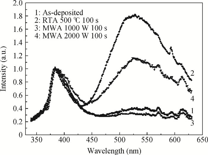
Table 1. ALD process parameters for ZnO thin films.

|
Table 2. The data evaluated from XRD patterns of the as-deposited and the ZnO thin films annealed for a fixed 100 s at different annealing conditions.

|
| [1] |
Hoffman R L, Norris B J, Wager J F. ZnO-based transparent thin-film transistors. Appl Phys Lett, 2003, 82(5):733 doi: 10.1063/1.1542677
|
| [2] |
Fortunato E M C, Barquinha P M C, Pimentel A C M B G, et al. Fully transparent ZnO thin-film transistor produced at room temperature. Adv Mater, 2005, 17(5):590 doi: 10.1002/adma.200400368
|
| [3] |
Carcia P, McLean R, Reilly M. High-performance ZnO thin-film transistors on gate dielectrics grown by atomic layer deposition. Appl Phys Lett, 2006, 88(12):123509 doi: 10.1063/1.2188379
|
| [4] |
Bayraktaroglu B, Leedy K, Neidhard R. Microwave ZnO thin-film transistors. IEEE Electron Device Lett, 2008, 29(9):1024 doi: 10.1109/LED.2008.2001635
|
| [5] |
Fortunato E, Barquinha P, Martins R. Oxide semiconductor thin-film transistors:a review of recent advances. Adv Mater, 2012, 24(22):2945 doi: 10.1002/adma.v24.22
|
| [6] |
Chiang H Q, Wager J F, Hoffman R L, et al. High mobility transparent thin-film transistors with amorphous zinc tin oxide channel layer. Appl Phys Lett, 2005, 86(1):013503 doi: 10.1063/1.1843286
|
| [7] |
Law M, Greene L E, Johnson J C, et al. Nanowire dye-sensitized solar cells. Nature Mater, 2005, 4(6):455 doi: 10.1038/nmat1387
|
| [8] |
Lee Y C, Hu S Y, Water W, et al. Improved optical and structural properties of ZnO thin films by rapid thermal annealing. Solid State Commun, 2007, 143(4/5):250 http://www.sciencedirect.com/science/article/pii/S0038109807003821
|
| [9] |
Hong R, Huang J, He H, et al. Influence of different post-treatments on the structure and optical properties of zinc oxide thin films. Appl Surf Sci, 2005, 242(3):346 http://www.sciencedirect.com/science/article/pii/S0169433204013303
|
| [10] |
Abdelouahab G, Benramache S, Benhaoua B, et al. Preparation of transparent conducting ZnO:Al films on glass substrates by ultrasonic spray technique. Journal of Semiconductors, 2013, 34(7):073002 doi: 10.1088/1674-4926/34/7/073002
|
| [11] |
Pung S Y, Choy K L, Shan C. Preferential growth of ZnO thin films by the atomic layer deposition technique. Nanotechnology, 2008, 19(43):435609 doi: 10.1088/0957-4484/19/43/435609
|
| [12] |
Kang H S, Kang J S, Kim J W, et al. Annealing effect on the property of ultraviolet and green emissions of ZnO thin films. J Appl Phys, 2004, 95(3):1246 doi: 10.1063/1.1633343
|
| [13] |
Wang M, Wang J, Chen W, et al. Effect of preheating and annealing temperatures on quality characteristics of ZnO thin film prepared by sol-gel method. Mater Chem Phys, 2006, 97(2):219 http://www.sciencedirect.com/science/article/pii/S0254058405004980
|
| [14] |
Lee Y C, Hu S Y, Water W, et al. Rapid thermal annealing effects on the structural and optical properties of ZnO films deposited on Si substrates. J Luminescence, 2009, 129(2):148 doi: 10.1016/j.jlumin.2008.09.003
|
| [15] |
Cheng Y C. Effects of post-deposition rapid thermal annealing on aluminum-doped ZnO thin films grown by atomic layer deposition. Appl Surf Sci, 2011, 258(1):604 doi: 10.1016/j.apsusc.2011.07.124
|
| [16] |
Wen Zhanhua, Wang Li, Fang Wenqing, et al. Influence of annealing temperature on strucatural and optical properites of ZnO thin films. Chinese Journal of Semiconductors, 2005, 26(3):498(in Chinese) http://en.cnki.com.cn/Article_en/CJFDTOTAL-BDTX20050300D.htm
|
| [17] |
Xu P, Fu C, Hu C, et al. Ultra-shallow junctions formed using microwave annealing. Appl Phys Lett, 2013, 102(12):112114 doi: 10.1063/1.4799030
|
| [18] |
Yeh M S, Lee Y J, Hung M F, et al. High-performance gate-all-around poly-Si thin-film transistors by microwave annealing with NH3 plasma passivation. IEEE Trans Nanotechnol, 2013, 12(4):636 doi: 10.1109/TNANO.2013.2265778
|
| [19] |
Cho T C, Lu Y L, Yao J Y, et al. Microwave annealing of phosphorus and cluster carbon implanted (100) and (110) Si. ECS Journal of Solid State Science and Technology, 2013, 2(7):293 doi: 10.1149/2.010307jss
|
| [20] |
Cui M L, Wu X M, Zhuge L J, et al. Effects of annealing temperature on the structure and photoluminescence properties of ZnO films. Vacuum, 2007, 81(7):899 doi: 10.1016/j.vacuum.2006.10.011
|
| [21] |
Kukreja L M, Misra P, Fallert P, et al. Correlation of spectral features of photoluminescence with residual native defects of ZnO thin films annealed at different temperatures. J Appl Phys, 2012, 112(1):013525 doi: 10.1063/1.4730774
|
| [22] |
Fang Z B, Yan Z J, Tan Y S, et al. Influence of post-annealing treatment on the structure properties of ZnO films. Appl Surf Sci, 2005, 241(3/4):303 doi: 10.1007/11551362_64
|
| [23] |
Kang H S, Kang J S, Pang S S, et al. Variation of light emitting properties of ZnO thin films depending on post-annealing temperature. Mater Sci Eng B, 2003, 102(1-3):313 doi: 10.1016/S0921-5107(02)00730-4
|
| [24] |
Lin B, Fu Z, Jia Y. Green luminescent center in undoped zinc oxide films deposited on silicon substrates. Appl Phys Lett, 2001, 79(7):943 doi: 10.1063/1.1394173
|


Article views: 3740 Times PDF downloads: 63 Times Cited by: 0 Times
Received: 30 April 2014 Revised: 17 June 2014 Online: Published: 01 November 2014
| Citation: |
Shirui Zhao, Yabin Dong, Mingyan Yu, Xiaolong Guo, Xinwei Xu, Yupeng Jing, Yang Xia. Microwave annealing effects on ZnO films deposited by atomic layer deposition[J]. Journal of Semiconductors, 2014, 35(11): 112001. doi: 10.1088/1674-4926/35/11/112001
****
S R Zhao, Y B Dong, M Y Yu, X L Guo, X W Xu, Y P Jing, Y Xia. Microwave annealing effects on ZnO films deposited by atomic layer deposition[J]. J. Semicond., 2014, 35(11): 112001. doi: 10.1088/1674-4926/35/11/112001.

|
| [1] |
Hoffman R L, Norris B J, Wager J F. ZnO-based transparent thin-film transistors. Appl Phys Lett, 2003, 82(5):733 doi: 10.1063/1.1542677
|
| [2] |
Fortunato E M C, Barquinha P M C, Pimentel A C M B G, et al. Fully transparent ZnO thin-film transistor produced at room temperature. Adv Mater, 2005, 17(5):590 doi: 10.1002/adma.200400368
|
| [3] |
Carcia P, McLean R, Reilly M. High-performance ZnO thin-film transistors on gate dielectrics grown by atomic layer deposition. Appl Phys Lett, 2006, 88(12):123509 doi: 10.1063/1.2188379
|
| [4] |
Bayraktaroglu B, Leedy K, Neidhard R. Microwave ZnO thin-film transistors. IEEE Electron Device Lett, 2008, 29(9):1024 doi: 10.1109/LED.2008.2001635
|
| [5] |
Fortunato E, Barquinha P, Martins R. Oxide semiconductor thin-film transistors:a review of recent advances. Adv Mater, 2012, 24(22):2945 doi: 10.1002/adma.v24.22
|
| [6] |
Chiang H Q, Wager J F, Hoffman R L, et al. High mobility transparent thin-film transistors with amorphous zinc tin oxide channel layer. Appl Phys Lett, 2005, 86(1):013503 doi: 10.1063/1.1843286
|
| [7] |
Law M, Greene L E, Johnson J C, et al. Nanowire dye-sensitized solar cells. Nature Mater, 2005, 4(6):455 doi: 10.1038/nmat1387
|
| [8] |
Lee Y C, Hu S Y, Water W, et al. Improved optical and structural properties of ZnO thin films by rapid thermal annealing. Solid State Commun, 2007, 143(4/5):250 http://www.sciencedirect.com/science/article/pii/S0038109807003821
|
| [9] |
Hong R, Huang J, He H, et al. Influence of different post-treatments on the structure and optical properties of zinc oxide thin films. Appl Surf Sci, 2005, 242(3):346 http://www.sciencedirect.com/science/article/pii/S0169433204013303
|
| [10] |
Abdelouahab G, Benramache S, Benhaoua B, et al. Preparation of transparent conducting ZnO:Al films on glass substrates by ultrasonic spray technique. Journal of Semiconductors, 2013, 34(7):073002 doi: 10.1088/1674-4926/34/7/073002
|
| [11] |
Pung S Y, Choy K L, Shan C. Preferential growth of ZnO thin films by the atomic layer deposition technique. Nanotechnology, 2008, 19(43):435609 doi: 10.1088/0957-4484/19/43/435609
|
| [12] |
Kang H S, Kang J S, Kim J W, et al. Annealing effect on the property of ultraviolet and green emissions of ZnO thin films. J Appl Phys, 2004, 95(3):1246 doi: 10.1063/1.1633343
|
| [13] |
Wang M, Wang J, Chen W, et al. Effect of preheating and annealing temperatures on quality characteristics of ZnO thin film prepared by sol-gel method. Mater Chem Phys, 2006, 97(2):219 http://www.sciencedirect.com/science/article/pii/S0254058405004980
|
| [14] |
Lee Y C, Hu S Y, Water W, et al. Rapid thermal annealing effects on the structural and optical properties of ZnO films deposited on Si substrates. J Luminescence, 2009, 129(2):148 doi: 10.1016/j.jlumin.2008.09.003
|
| [15] |
Cheng Y C. Effects of post-deposition rapid thermal annealing on aluminum-doped ZnO thin films grown by atomic layer deposition. Appl Surf Sci, 2011, 258(1):604 doi: 10.1016/j.apsusc.2011.07.124
|
| [16] |
Wen Zhanhua, Wang Li, Fang Wenqing, et al. Influence of annealing temperature on strucatural and optical properites of ZnO thin films. Chinese Journal of Semiconductors, 2005, 26(3):498(in Chinese) http://en.cnki.com.cn/Article_en/CJFDTOTAL-BDTX20050300D.htm
|
| [17] |
Xu P, Fu C, Hu C, et al. Ultra-shallow junctions formed using microwave annealing. Appl Phys Lett, 2013, 102(12):112114 doi: 10.1063/1.4799030
|
| [18] |
Yeh M S, Lee Y J, Hung M F, et al. High-performance gate-all-around poly-Si thin-film transistors by microwave annealing with NH3 plasma passivation. IEEE Trans Nanotechnol, 2013, 12(4):636 doi: 10.1109/TNANO.2013.2265778
|
| [19] |
Cho T C, Lu Y L, Yao J Y, et al. Microwave annealing of phosphorus and cluster carbon implanted (100) and (110) Si. ECS Journal of Solid State Science and Technology, 2013, 2(7):293 doi: 10.1149/2.010307jss
|
| [20] |
Cui M L, Wu X M, Zhuge L J, et al. Effects of annealing temperature on the structure and photoluminescence properties of ZnO films. Vacuum, 2007, 81(7):899 doi: 10.1016/j.vacuum.2006.10.011
|
| [21] |
Kukreja L M, Misra P, Fallert P, et al. Correlation of spectral features of photoluminescence with residual native defects of ZnO thin films annealed at different temperatures. J Appl Phys, 2012, 112(1):013525 doi: 10.1063/1.4730774
|
| [22] |
Fang Z B, Yan Z J, Tan Y S, et al. Influence of post-annealing treatment on the structure properties of ZnO films. Appl Surf Sci, 2005, 241(3/4):303 doi: 10.1007/11551362_64
|
| [23] |
Kang H S, Kang J S, Pang S S, et al. Variation of light emitting properties of ZnO thin films depending on post-annealing temperature. Mater Sci Eng B, 2003, 102(1-3):313 doi: 10.1016/S0921-5107(02)00730-4
|
| [24] |
Lin B, Fu Z, Jia Y. Green luminescent center in undoped zinc oxide films deposited on silicon substrates. Appl Phys Lett, 2001, 79(7):943 doi: 10.1063/1.1394173
|

 WeChat ID
Journal of Semiconductors © 2017 All Rights Reserved 京ICP备05085259号-2

 DownLoad:

