


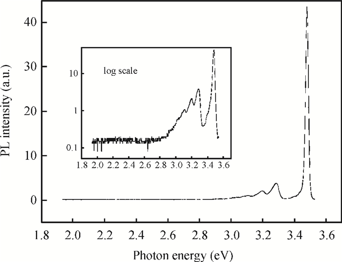
Fig. 1.
Photoluminescence spectra of the control sample at 10 K. The log scale spectrum is also shown. Yellow luminescence is not very visible in this sample.
SEMICONDUCTOR MATERIALS
Z. Mouffak1, , A. Bensaoula2 and L. Trombetta3
Corresponding author: Z. Mouffak, Email:zmouffak@csufresno.edu
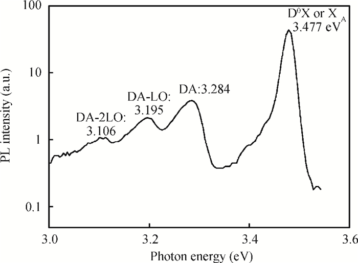
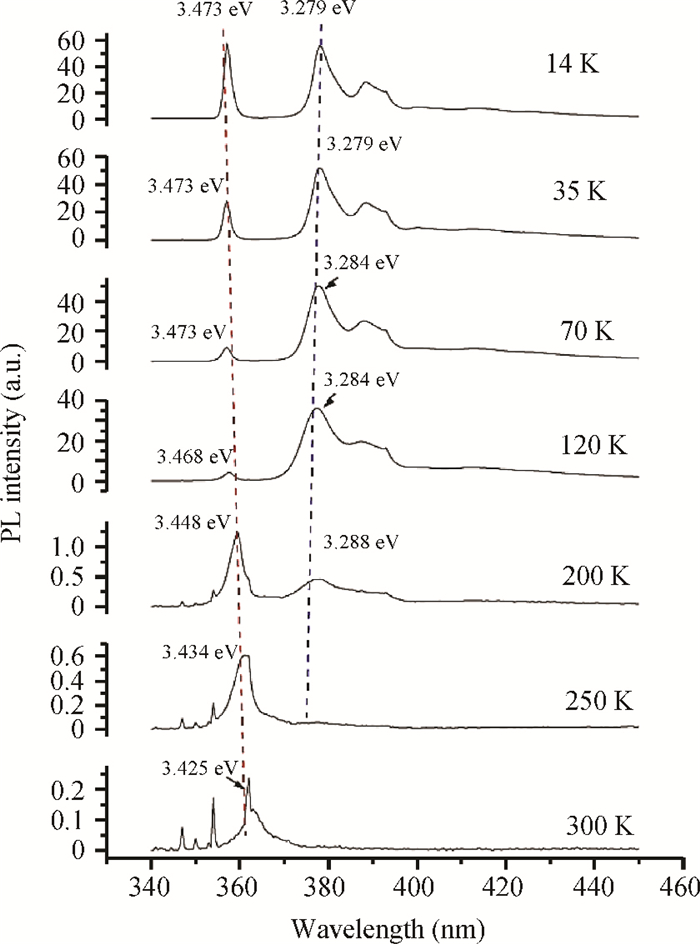
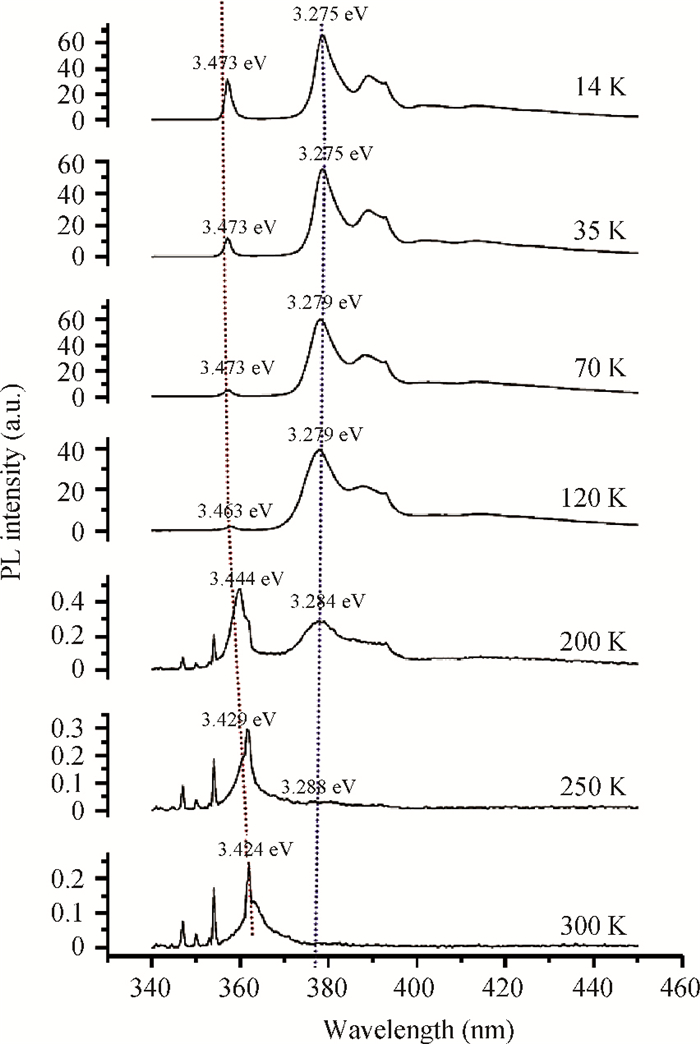
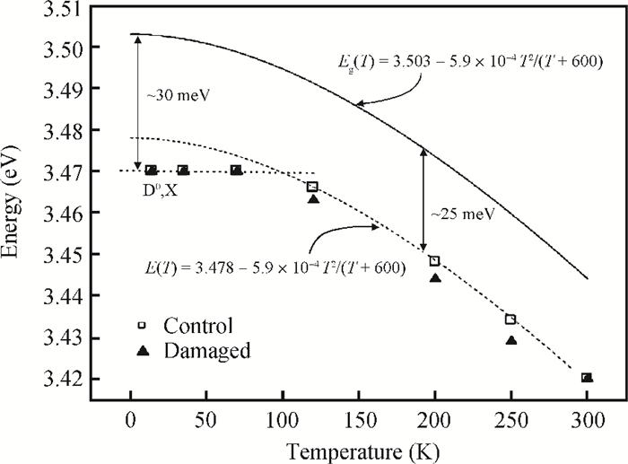
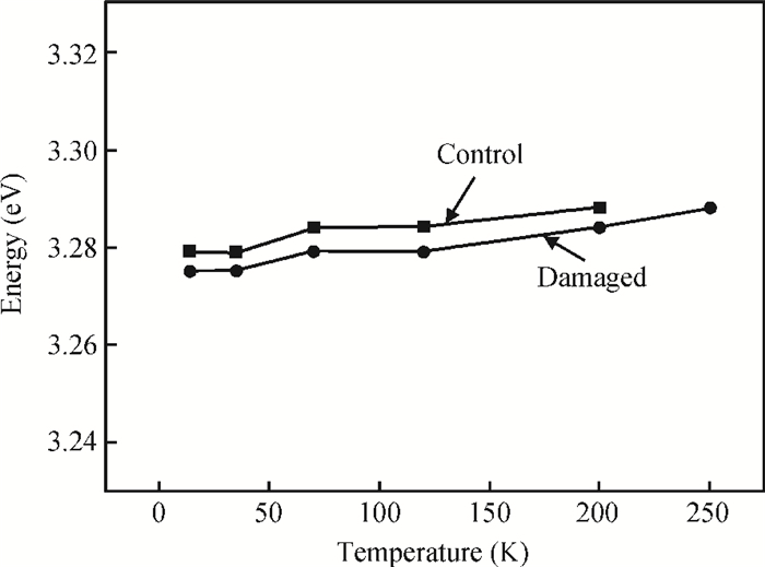
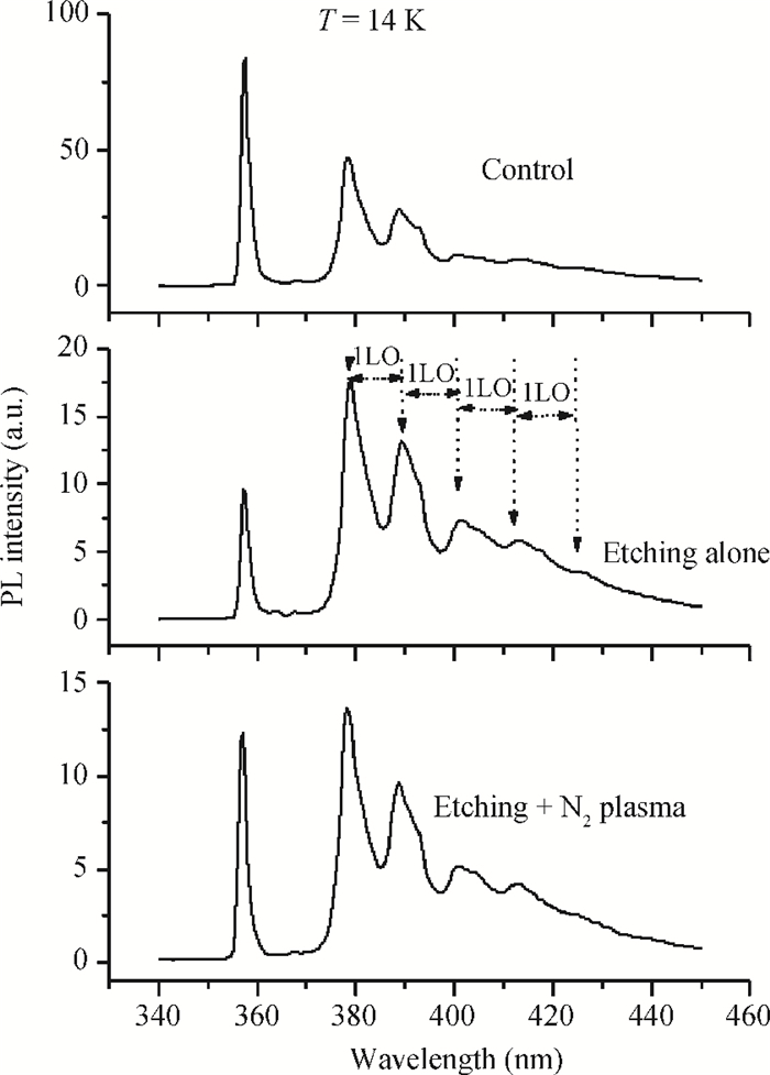
Abstract: GaN films with reactive ion etching (RIE) induced damage were analyzed using photoluminescence (PL). We observed band-edge as well as donor-acceptor peaks with associated phonon replicas, all in agreement with previous studies. While both the control and damaged samples have their band-edge peak location change with temperature following the Varshni formula, its intensity however decreases with damage while the D-A peak increases considerably. Nitrogen post-etch plasma was shown to improve the band edge peak and decrease the D-A peak. This suggests that the N2 plasma has helped reduce the number of trapped carriers that were participating in the D-A transition and made the D°X transition more active, which reaffirms the N2 post-etch plasma treatment as a good technique to heal the GaN surface, most likely by filling the nitrogen vacancies previously created by etch damage.
Keywords: GaN, etch damage, photoluminescence, reactive ion etching
| [1] |
Nakamura S, Mukai T, Senoh M. Candela-class high-brightness InGaN/AlGaN double-heterostructure blue-light-emitting diodes. Appl Phys Lett, 1994, 64:1687 doi: 10.1063/1.111832
|
| [2] |
Popovici G. Group Ⅲ nitride semiconductor compounds, physics and applications. Gil B, ed. Oxford:Clarendon Press, 1999
|
| [3] |
Wu Y F, Keller P B, Kapolnek D, et al. Very high breakdown voltage and large transconductance realized on GaN heterojunction field effect transistors. Appl Phys Lett, 1996, 69:1438 doi: 10.1063/1.117607
|
| [4] |
Morkoç H, Strite S, Gao G B, et al. Large-band-gap SiC, Ⅲ-Ⅴ nitride, and Ⅱ-Ⅵ ZnSe-based semiconductor device technologies. J Appl Phys, 1994, 76:1363 doi: 10.1063/1.358463
|
| [5] |
Morkoç H. Nitride semiconductors and devices. Springer, Berlin, Heidelberg:Springer Series in Material Science, 1999 doi: 10.1007/978-3-642-58562-3.pdf
|
| [6] |
Pearton S J, Vartuli C B, Zolper J C, et al. Ion implantation doping and isolation of GaN. Appl Phys Lett, 1995, 67:1435 doi: 10.1063/1.114518
|
| [7] |
Strite S, Morkoç H. GaN, AlN, and InN:a review. J Vac Sci Technol B, 1992, 10:1237 doi: 10.1116/1.585897
|
| [8] |
Goldenberg B, Zook J D, Ulmer R J. Ultraviolet and violet light-emitting GaN diodes grown by low-pressure metalorganic chemical vapor deposition. Appl Phys Lett, 1993, 62:381 doi: 10.1063/1.108963
|
| [9] |
Mouffak Z, Medelci-Djezzar N, Boney C, et al. Effect of photo-assisted RIE damage on GaN. MRS Internet J Nitride Semicond Res, 2003, 8:7 doi: 10.1557/S1092578300000508
|
| [10] |
Mouffak Z, Bensaoula A, Trombetta L. Temperature dependence of the energy gap in semiconductors. J Appl Phys, 2004, 95:727 doi: 10.1063/1.1632552
|
| [11] |
Hwang S J, Cho Y H, Song J J, et al. Photoluminescence excitation study of LO-phonon assisted excitonic transitions in GaN. MRS Proceedings, 1997, 482:691 doi: 10.1557/PROC-482-691
|
| [12] |
Fischer S, Wetzel C, Haller E E, et al. On p-type doping in GaN-acceptor binding energies. Appl Phys Lett, 1995, 67:1298 doi: 10.1063/1.114403
|
| [13] |
Götz W, Johnson N M, Chen C, et al. Activation energies of Si donors in GaN. Appl Phys Lett, 1996, 68:3144 doi: 10.1063/1.115805
|
| [14] |
Philippe A. Electro-optical characterization of hexagonal and cubic gallium nitride for blue emitters application. PhD Dissertation, Institut National des Sciences Appliquées (INSA) de Lyon, 1999
|
| [15] |
Varshni Y P. Temperature dependence of the energy gap in semiconductors. Physica, 1967, 34:149 doi: 10.1016/0031-8914(67)90062-6
|
| [16] |
Monemar B. Fundamental energy gap of GaN from photoluminescence excitation spectra. Phys Rev B, 1974, 10:676 doi: 10.1103/PhysRevB.10.676
|
| [17] |
Gil B, Briot O, Aulombard R L. Valence-band physics and the optical properties of GaN epilayers grown onto sapphire with wurtzite symmetry. Phys Rev B, 1995, 52:17028 doi: 10.1103/PhysRevB.52.R17028
|
| [18] |
Merz C, Kunzer M, Kaufmann U. Free and bound excitons in thin wurtzite GaN layers on sapphire. Semicond Sci Tech, 1996, 11:712 doi: 10.1088/0268-1242/11/5/010
|
| [19] |
Xu S J, Liu W, Li M F. Direct determination of free exciton binding energy from phonon-assisted luminescence spectra in GaN epilayers. Appl Phys Lett, 2002, 81:2959 doi: 10.1063/1.1514391
|


Article views: 3857 Times PDF downloads: 48 Times Cited by: 0 Times
Received: 26 May 2014 Revised: 10 July 2014 Online: Published: 01 November 2014
| Citation: |
Z. Mouffak, A. Bensaoula, L. Trombetta. A photoluminescence study of plasma reactive ion etching-induced damage in GaN[J]. Journal of Semiconductors, 2014, 35(11): 113003. doi: 10.1088/1674-4926/35/11/113003
****
Z. Mouffak, A. Bensaoula, L. Trombetta. A photoluminescence study of plasma reactive ion etching-induced damage in GaN[J]. J. Semicond., 2014, 35(11): 113003. doi: 10.1088/1674-4926/35/11/113003.

|
| [1] |
Nakamura S, Mukai T, Senoh M. Candela-class high-brightness InGaN/AlGaN double-heterostructure blue-light-emitting diodes. Appl Phys Lett, 1994, 64:1687 doi: 10.1063/1.111832
|
| [2] |
Popovici G. Group Ⅲ nitride semiconductor compounds, physics and applications. Gil B, ed. Oxford:Clarendon Press, 1999
|
| [3] |
Wu Y F, Keller P B, Kapolnek D, et al. Very high breakdown voltage and large transconductance realized on GaN heterojunction field effect transistors. Appl Phys Lett, 1996, 69:1438 doi: 10.1063/1.117607
|
| [4] |
Morkoç H, Strite S, Gao G B, et al. Large-band-gap SiC, Ⅲ-Ⅴ nitride, and Ⅱ-Ⅵ ZnSe-based semiconductor device technologies. J Appl Phys, 1994, 76:1363 doi: 10.1063/1.358463
|
| [5] |
Morkoç H. Nitride semiconductors and devices. Springer, Berlin, Heidelberg:Springer Series in Material Science, 1999 doi: 10.1007/978-3-642-58562-3.pdf
|
| [6] |
Pearton S J, Vartuli C B, Zolper J C, et al. Ion implantation doping and isolation of GaN. Appl Phys Lett, 1995, 67:1435 doi: 10.1063/1.114518
|
| [7] |
Strite S, Morkoç H. GaN, AlN, and InN:a review. J Vac Sci Technol B, 1992, 10:1237 doi: 10.1116/1.585897
|
| [8] |
Goldenberg B, Zook J D, Ulmer R J. Ultraviolet and violet light-emitting GaN diodes grown by low-pressure metalorganic chemical vapor deposition. Appl Phys Lett, 1993, 62:381 doi: 10.1063/1.108963
|
| [9] |
Mouffak Z, Medelci-Djezzar N, Boney C, et al. Effect of photo-assisted RIE damage on GaN. MRS Internet J Nitride Semicond Res, 2003, 8:7 doi: 10.1557/S1092578300000508
|
| [10] |
Mouffak Z, Bensaoula A, Trombetta L. Temperature dependence of the energy gap in semiconductors. J Appl Phys, 2004, 95:727 doi: 10.1063/1.1632552
|
| [11] |
Hwang S J, Cho Y H, Song J J, et al. Photoluminescence excitation study of LO-phonon assisted excitonic transitions in GaN. MRS Proceedings, 1997, 482:691 doi: 10.1557/PROC-482-691
|
| [12] |
Fischer S, Wetzel C, Haller E E, et al. On p-type doping in GaN-acceptor binding energies. Appl Phys Lett, 1995, 67:1298 doi: 10.1063/1.114403
|
| [13] |
Götz W, Johnson N M, Chen C, et al. Activation energies of Si donors in GaN. Appl Phys Lett, 1996, 68:3144 doi: 10.1063/1.115805
|
| [14] |
Philippe A. Electro-optical characterization of hexagonal and cubic gallium nitride for blue emitters application. PhD Dissertation, Institut National des Sciences Appliquées (INSA) de Lyon, 1999
|
| [15] |
Varshni Y P. Temperature dependence of the energy gap in semiconductors. Physica, 1967, 34:149 doi: 10.1016/0031-8914(67)90062-6
|
| [16] |
Monemar B. Fundamental energy gap of GaN from photoluminescence excitation spectra. Phys Rev B, 1974, 10:676 doi: 10.1103/PhysRevB.10.676
|
| [17] |
Gil B, Briot O, Aulombard R L. Valence-band physics and the optical properties of GaN epilayers grown onto sapphire with wurtzite symmetry. Phys Rev B, 1995, 52:17028 doi: 10.1103/PhysRevB.52.R17028
|
| [18] |
Merz C, Kunzer M, Kaufmann U. Free and bound excitons in thin wurtzite GaN layers on sapphire. Semicond Sci Tech, 1996, 11:712 doi: 10.1088/0268-1242/11/5/010
|
| [19] |
Xu S J, Liu W, Li M F. Direct determination of free exciton binding energy from phonon-assisted luminescence spectra in GaN epilayers. Appl Phys Lett, 2002, 81:2959 doi: 10.1063/1.1514391
|

 WeChat ID
Journal of Semiconductors © 2017 All Rights Reserved 京ICP备05085259号-2

 DownLoad:

