


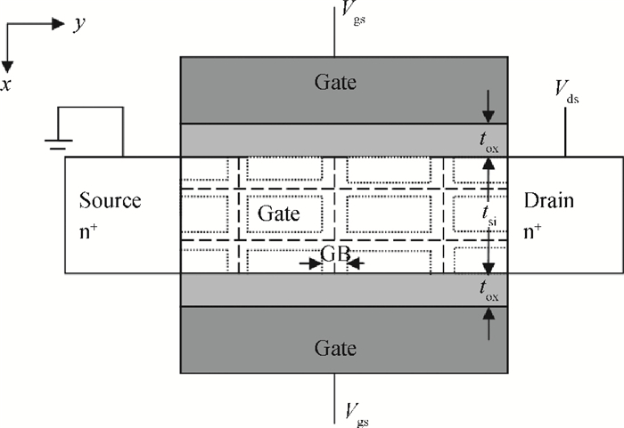
Fig. 1.
Diagram of the structure of an undoped SDG poly-Si TFT.
SEMICONDUCTOR PHYSICS
Abstract: A physical and explicit surface potential model for undoped symmetric double-gate polysilicon thin-film transistors has been derived based on an effective charge density approach of Poisson's equation with both exponential deep and tail state terms included. The proposed surface potential calculation is single-piece and eliminates the regional approach. Model predictions are compared to numerical simulations with close agreement, having absolute error in the millivolt range. Furthermore, expressions of the drain current are given for a wide range of operation regions, which have been justified by thorough comparisons with experimental data.
Keywords: double-gate, drain current, surface potential, polysilicon thin-film transistor
| [1] |
Moschou D C, Theodorou C G, Hastas N A, et al.Short channel effects on LTPS TFT degradation. Journal of Display Technology, 2013, PP(99):1 https://www.osapublishing.org/jdt/abstract.cfm?uri=jdt-9-9-747
|
| [2] |
Tsai C C, Lee Y J, Wang J L, et al. High-performance top and bottom double-gate low temperature poly-silicon thin film transistors fabricated by excimer laser crystallization. Solid State Electron, 2008, 52(3):365 doi: 10.1016/j.sse.2007.10.029
|
| [3] |
Zhang S, Han R, Sin J K O, et al. A novel self-aligned double-gate TFT technology. IEEE Electron Device Lett., 2001, 22(11):530. doi: 10.1109/55.962653
|
| [4] |
Tsai C C, Wei K F, Lee Y J, et al. High-performance short-channel double-gate lowtemperature polysilicon thin-film transistors using excimer laser crystallization. IEEE Electron Device Lett, 2007, 28(11):1010 doi: 10.1109/LED.2007.908473
|
| [5] |
Lin H C, Lin Z M, Chen W C, et al. Read characteristics of independent double-gate poly-Si nanowire SONOS devices. IEEE Trans. Electron Devices, 2011, 58(11):3771 doi: 10.1109/TED.2011.2164251
|
| [6] |
Tsuji H, Kuzuoka H, Kishida Y, et al. Surface-potential-based drain current model for polycrystalline silicon thin-film transistors. Jpa J Appl Phys, 2008, 47(10):7798 doi: 10.1143/JJAP.47.7798
|
| [7] |
Chen R, Zheng X, Deng W, et al. A physical-based analytical solution tot the surface potential of polysilicon thin film transistors using the Lambert W function. Solid-State Electron, 2007, 51(6):975 doi: 10.1016/j.sse.2007.03.004
|
| [8] |
Sehgal A, Mangla T, Chopra S, et al. Physics based threshold voltage extraction and simulation for poly-crystalline thin film transistors using a double-gate structure. Semicond Sci Technol, 2006, 21(3):370 doi: 10.1088/0268-1242/21/3/028
|
| [9] |
Wang L, Ren Y, Han D, et al. Asynchronous double-gate polycrystalline silicon thin-film transistors for AM-OLED pixel circuits. IEEE 11th International Conference on Solid-State and Integrated Circuit Technology (ICSICT), 2012, DOI: 10.1109/ICSICT.2012.6467841
|
| [10] |
Huang J, Deng W, Zheng X, et al. A compact model for undoped symmetric double-gate polysilicon thin-film transistors. IEEE Trans Electron Devices, 2010, 57(10):2607 doi: 10.1109/TED.2010.2060725
|
| [11] |
Deng W, Zheng X, Chen R. A new poly-Si TFTs DC model for device characterization and circuit simulation. Chinese Journal of Semiconductors, 2007, 28(12):1916
|
| [12] |
Ortiz-Conde A, García-Sánchez F J, Muci J, et al. A review of core compact models for undoped double-gate SOI MOSFETs. IEEE Trans Electron Devices, 2007, 54(1):131 doi: 10.1109/TED.2006.887046
|
| [13] |
Sallese J M, Chevillon N, Lallement C, et al. Charge-based modeling of junctionless double-gate field-effect transistors. IEEE Trans Electron Devices, 2011, 58(8):2628 doi: 10.1109/TED.2011.2156413
|
| [14] |
Ortiz-Conde A, García-Sánchez F J, Malobabic S. Analytic solution of the channel potential in undoped symmetric dual-gate MOSFETs. IEEE Trans Electron Devices, 2005, 52(7):1669 doi: 10.1109/TED.2005.850629
|
| [15] |
Ortiz-Conde A, García-Sánchez F J, Muci J. Rigorous analytic solution for the drain current of undoped symmetric dual-gate MOSFETs. Solid State Electron, 2005, 49(4):640 doi: 10.1016/j.sse.2005.01.017
|
| [16] |
He J, Liu F, Zhou X, et al. A continuous analytic channel potential solution to doped symmetric double-gate MOSFETs from the accumulation to the strong-inversion region. Chin Phys B, 2011, 20(1):016102 doi: 10.1088/1674-1056/20/1/016102
|
| [17] |
He J, Zhang L, Zhang J, et al. A complete surface potential-based core model for undoped symmetric double-gate MOSFETs. Journal of Semiconductors, 2008, 29(11):2092 http://www.jos.ac.cn/bdtxbcn/ch/reader/view_abstract.aspx?file_no=08052001&flag=1
|
| [18] |
Jacunski M D, Shurn M S, Owusu A A, et al. A short-channel DC SPICE model for polysilicon thin-film transistors including temperature effects. IEEE Trans Electron Devices, 1999, 46(6):1146 doi: 10.1109/16.766877
|
| [19] |
Park J H, Kim Y, Kim S, et al. Surface-potential-based analytic DC I——V model with effective electron density for a-IGZO TFTs considering the parasitic resistance. IEEE Electron Device Lett, 2011, 32(11):1540 doi: 10.1109/LED.2011.2163810
|
| [20] |
Wang M, Wong M. An effective channel mobility-based analytical on-current model for polycrystalline silicon thin-film transistors. IEEE Trans Electron Devices, 2007, 54(4):869 doi: 10.1109/TED.2007.891248
|
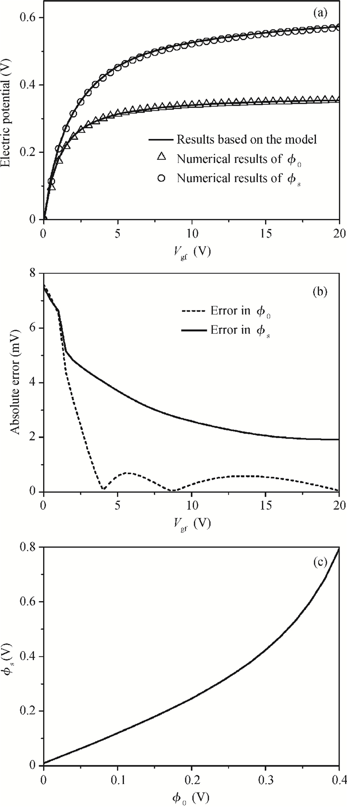
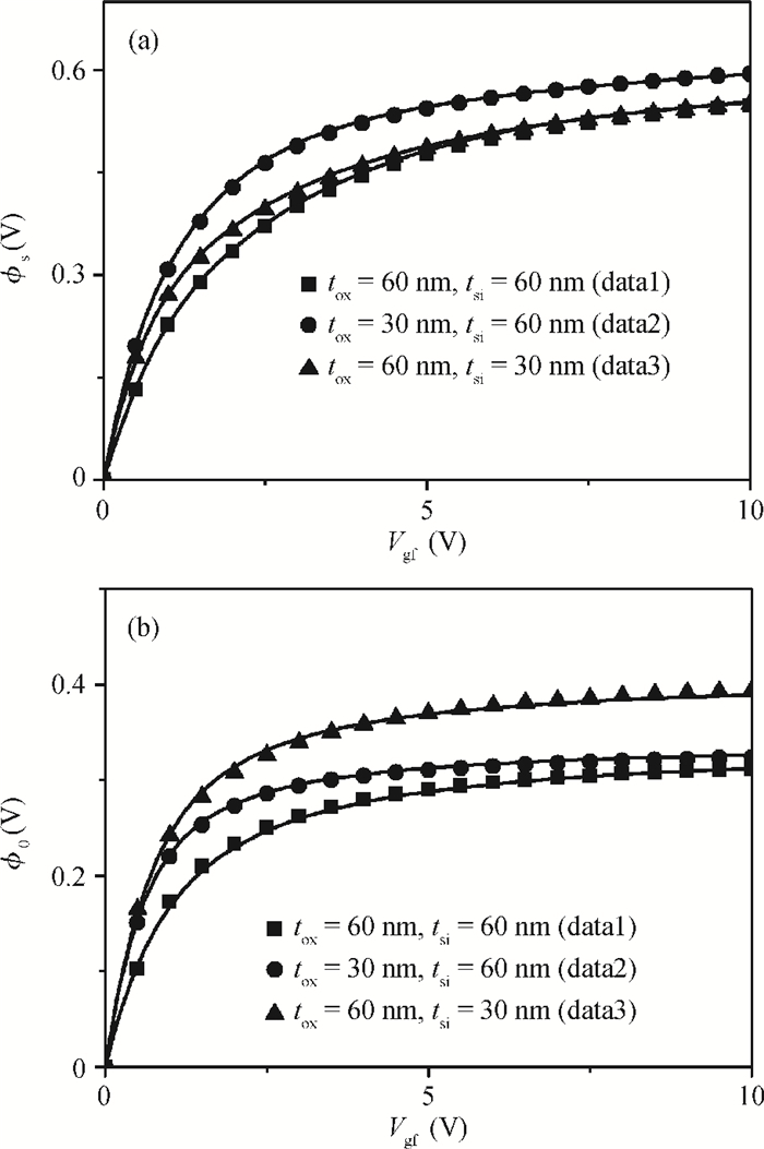
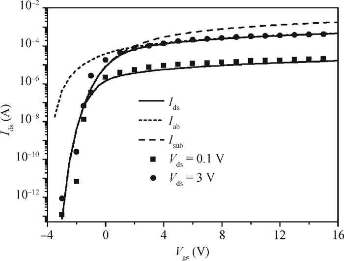
Table 1. Parameters used for simulation in Fig. 2.

|
Table 2. Parameters used for simulation in Fig. 3.

|
Table 3. Parameters used for simulation in Fig. 4.

|
Table 4. Parameters used for simulation in Fig. 5.

|
| [1] |
Moschou D C, Theodorou C G, Hastas N A, et al.Short channel effects on LTPS TFT degradation. Journal of Display Technology, 2013, PP(99):1 https://www.osapublishing.org/jdt/abstract.cfm?uri=jdt-9-9-747
|
| [2] |
Tsai C C, Lee Y J, Wang J L, et al. High-performance top and bottom double-gate low temperature poly-silicon thin film transistors fabricated by excimer laser crystallization. Solid State Electron, 2008, 52(3):365 doi: 10.1016/j.sse.2007.10.029
|
| [3] |
Zhang S, Han R, Sin J K O, et al. A novel self-aligned double-gate TFT technology. IEEE Electron Device Lett., 2001, 22(11):530. doi: 10.1109/55.962653
|
| [4] |
Tsai C C, Wei K F, Lee Y J, et al. High-performance short-channel double-gate lowtemperature polysilicon thin-film transistors using excimer laser crystallization. IEEE Electron Device Lett, 2007, 28(11):1010 doi: 10.1109/LED.2007.908473
|
| [5] |
Lin H C, Lin Z M, Chen W C, et al. Read characteristics of independent double-gate poly-Si nanowire SONOS devices. IEEE Trans. Electron Devices, 2011, 58(11):3771 doi: 10.1109/TED.2011.2164251
|
| [6] |
Tsuji H, Kuzuoka H, Kishida Y, et al. Surface-potential-based drain current model for polycrystalline silicon thin-film transistors. Jpa J Appl Phys, 2008, 47(10):7798 doi: 10.1143/JJAP.47.7798
|
| [7] |
Chen R, Zheng X, Deng W, et al. A physical-based analytical solution tot the surface potential of polysilicon thin film transistors using the Lambert W function. Solid-State Electron, 2007, 51(6):975 doi: 10.1016/j.sse.2007.03.004
|
| [8] |
Sehgal A, Mangla T, Chopra S, et al. Physics based threshold voltage extraction and simulation for poly-crystalline thin film transistors using a double-gate structure. Semicond Sci Technol, 2006, 21(3):370 doi: 10.1088/0268-1242/21/3/028
|
| [9] |
Wang L, Ren Y, Han D, et al. Asynchronous double-gate polycrystalline silicon thin-film transistors for AM-OLED pixel circuits. IEEE 11th International Conference on Solid-State and Integrated Circuit Technology (ICSICT), 2012, DOI: 10.1109/ICSICT.2012.6467841
|
| [10] |
Huang J, Deng W, Zheng X, et al. A compact model for undoped symmetric double-gate polysilicon thin-film transistors. IEEE Trans Electron Devices, 2010, 57(10):2607 doi: 10.1109/TED.2010.2060725
|
| [11] |
Deng W, Zheng X, Chen R. A new poly-Si TFTs DC model for device characterization and circuit simulation. Chinese Journal of Semiconductors, 2007, 28(12):1916
|
| [12] |
Ortiz-Conde A, García-Sánchez F J, Muci J, et al. A review of core compact models for undoped double-gate SOI MOSFETs. IEEE Trans Electron Devices, 2007, 54(1):131 doi: 10.1109/TED.2006.887046
|
| [13] |
Sallese J M, Chevillon N, Lallement C, et al. Charge-based modeling of junctionless double-gate field-effect transistors. IEEE Trans Electron Devices, 2011, 58(8):2628 doi: 10.1109/TED.2011.2156413
|
| [14] |
Ortiz-Conde A, García-Sánchez F J, Malobabic S. Analytic solution of the channel potential in undoped symmetric dual-gate MOSFETs. IEEE Trans Electron Devices, 2005, 52(7):1669 doi: 10.1109/TED.2005.850629
|
| [15] |
Ortiz-Conde A, García-Sánchez F J, Muci J. Rigorous analytic solution for the drain current of undoped symmetric dual-gate MOSFETs. Solid State Electron, 2005, 49(4):640 doi: 10.1016/j.sse.2005.01.017
|
| [16] |
He J, Liu F, Zhou X, et al. A continuous analytic channel potential solution to doped symmetric double-gate MOSFETs from the accumulation to the strong-inversion region. Chin Phys B, 2011, 20(1):016102 doi: 10.1088/1674-1056/20/1/016102
|
| [17] |
He J, Zhang L, Zhang J, et al. A complete surface potential-based core model for undoped symmetric double-gate MOSFETs. Journal of Semiconductors, 2008, 29(11):2092 http://www.jos.ac.cn/bdtxbcn/ch/reader/view_abstract.aspx?file_no=08052001&flag=1
|
| [18] |
Jacunski M D, Shurn M S, Owusu A A, et al. A short-channel DC SPICE model for polysilicon thin-film transistors including temperature effects. IEEE Trans Electron Devices, 1999, 46(6):1146 doi: 10.1109/16.766877
|
| [19] |
Park J H, Kim Y, Kim S, et al. Surface-potential-based analytic DC I——V model with effective electron density for a-IGZO TFTs considering the parasitic resistance. IEEE Electron Device Lett, 2011, 32(11):1540 doi: 10.1109/LED.2011.2163810
|
| [20] |
Wang M, Wong M. An effective channel mobility-based analytical on-current model for polycrystalline silicon thin-film transistors. IEEE Trans Electron Devices, 2007, 54(4):869 doi: 10.1109/TED.2007.891248
|


Article views: 3720 Times PDF downloads: 24 Times Cited by: 0 Times
Received: 22 August 2013 Revised: 01 November 2013 Online: Published: 01 March 2014
| Citation: |
Xiaoyu Ma, Wanling Deng, Junkai Huang. Explicit solution of channel potential and drain current model in symmetric double-gate polysilicon TFTs[J]. Journal of Semiconductors, 2014, 35(3): 032002. doi: 10.1088/1674-4926/35/3/032002
****
X Y Ma, W L Deng, J K Huang. Explicit solution of channel potential and drain current model in symmetric double-gate polysilicon TFTs[J]. J. Semicond., 2014, 35(3): 032002. doi: 10.1088/1674-4926/35/3/032002.

|
| [1] |
Moschou D C, Theodorou C G, Hastas N A, et al.Short channel effects on LTPS TFT degradation. Journal of Display Technology, 2013, PP(99):1 https://www.osapublishing.org/jdt/abstract.cfm?uri=jdt-9-9-747
|
| [2] |
Tsai C C, Lee Y J, Wang J L, et al. High-performance top and bottom double-gate low temperature poly-silicon thin film transistors fabricated by excimer laser crystallization. Solid State Electron, 2008, 52(3):365 doi: 10.1016/j.sse.2007.10.029
|
| [3] |
Zhang S, Han R, Sin J K O, et al. A novel self-aligned double-gate TFT technology. IEEE Electron Device Lett., 2001, 22(11):530. doi: 10.1109/55.962653
|
| [4] |
Tsai C C, Wei K F, Lee Y J, et al. High-performance short-channel double-gate lowtemperature polysilicon thin-film transistors using excimer laser crystallization. IEEE Electron Device Lett, 2007, 28(11):1010 doi: 10.1109/LED.2007.908473
|
| [5] |
Lin H C, Lin Z M, Chen W C, et al. Read characteristics of independent double-gate poly-Si nanowire SONOS devices. IEEE Trans. Electron Devices, 2011, 58(11):3771 doi: 10.1109/TED.2011.2164251
|
| [6] |
Tsuji H, Kuzuoka H, Kishida Y, et al. Surface-potential-based drain current model for polycrystalline silicon thin-film transistors. Jpa J Appl Phys, 2008, 47(10):7798 doi: 10.1143/JJAP.47.7798
|
| [7] |
Chen R, Zheng X, Deng W, et al. A physical-based analytical solution tot the surface potential of polysilicon thin film transistors using the Lambert W function. Solid-State Electron, 2007, 51(6):975 doi: 10.1016/j.sse.2007.03.004
|
| [8] |
Sehgal A, Mangla T, Chopra S, et al. Physics based threshold voltage extraction and simulation for poly-crystalline thin film transistors using a double-gate structure. Semicond Sci Technol, 2006, 21(3):370 doi: 10.1088/0268-1242/21/3/028
|
| [9] |
Wang L, Ren Y, Han D, et al. Asynchronous double-gate polycrystalline silicon thin-film transistors for AM-OLED pixel circuits. IEEE 11th International Conference on Solid-State and Integrated Circuit Technology (ICSICT), 2012, DOI: 10.1109/ICSICT.2012.6467841
|
| [10] |
Huang J, Deng W, Zheng X, et al. A compact model for undoped symmetric double-gate polysilicon thin-film transistors. IEEE Trans Electron Devices, 2010, 57(10):2607 doi: 10.1109/TED.2010.2060725
|
| [11] |
Deng W, Zheng X, Chen R. A new poly-Si TFTs DC model for device characterization and circuit simulation. Chinese Journal of Semiconductors, 2007, 28(12):1916
|
| [12] |
Ortiz-Conde A, García-Sánchez F J, Muci J, et al. A review of core compact models for undoped double-gate SOI MOSFETs. IEEE Trans Electron Devices, 2007, 54(1):131 doi: 10.1109/TED.2006.887046
|
| [13] |
Sallese J M, Chevillon N, Lallement C, et al. Charge-based modeling of junctionless double-gate field-effect transistors. IEEE Trans Electron Devices, 2011, 58(8):2628 doi: 10.1109/TED.2011.2156413
|
| [14] |
Ortiz-Conde A, García-Sánchez F J, Malobabic S. Analytic solution of the channel potential in undoped symmetric dual-gate MOSFETs. IEEE Trans Electron Devices, 2005, 52(7):1669 doi: 10.1109/TED.2005.850629
|
| [15] |
Ortiz-Conde A, García-Sánchez F J, Muci J. Rigorous analytic solution for the drain current of undoped symmetric dual-gate MOSFETs. Solid State Electron, 2005, 49(4):640 doi: 10.1016/j.sse.2005.01.017
|
| [16] |
He J, Liu F, Zhou X, et al. A continuous analytic channel potential solution to doped symmetric double-gate MOSFETs from the accumulation to the strong-inversion region. Chin Phys B, 2011, 20(1):016102 doi: 10.1088/1674-1056/20/1/016102
|
| [17] |
He J, Zhang L, Zhang J, et al. A complete surface potential-based core model for undoped symmetric double-gate MOSFETs. Journal of Semiconductors, 2008, 29(11):2092 http://www.jos.ac.cn/bdtxbcn/ch/reader/view_abstract.aspx?file_no=08052001&flag=1
|
| [18] |
Jacunski M D, Shurn M S, Owusu A A, et al. A short-channel DC SPICE model for polysilicon thin-film transistors including temperature effects. IEEE Trans Electron Devices, 1999, 46(6):1146 doi: 10.1109/16.766877
|
| [19] |
Park J H, Kim Y, Kim S, et al. Surface-potential-based analytic DC I——V model with effective electron density for a-IGZO TFTs considering the parasitic resistance. IEEE Electron Device Lett, 2011, 32(11):1540 doi: 10.1109/LED.2011.2163810
|
| [20] |
Wang M, Wong M. An effective channel mobility-based analytical on-current model for polycrystalline silicon thin-film transistors. IEEE Trans Electron Devices, 2007, 54(4):869 doi: 10.1109/TED.2007.891248
|

 WeChat ID
Journal of Semiconductors © 2017 All Rights Reserved 京ICP备05085259号-2

 DownLoad:

