| Citation: |
Yang Tang, Zuochang Ye, Yan Wang. High efficiency modeling of broadband millimeter-wave CMOS FETs with gate width scalability by using pre-modeled cells[J]. Journal of Semiconductors, 2014, 35(3): 034012. doi: 10.1088/1674-4926/35/3/034012
****
Y Tang, Z C Ye, Y Wang. High efficiency modeling of broadband millimeter-wave CMOS FETs with gate width scalability by using pre-modeled cells[J]. J. Semicond., 2014, 35(3): 034012. doi: 10.1088/1674-4926/35/3/034012.
|
High efficiency modeling of broadband millimeter-wave CMOS FETs with gate width scalability by using pre-modeled cells
DOI: 10.1088/1674-4926/35/3/034012
More Information
-
Abstract
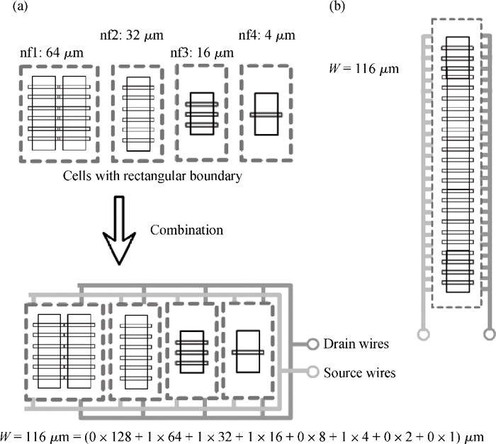
This work presents a highly efficient approach for broadband modeling of millimeter-wave CMOS FETs with gate width scalability by using pre-modeled cells. Only a few devices with varied gate width are required to be measured and modeled with fixed models, and later used as pre-modeled cells. Then a target device with the desired gate width is constructed by choosing appropriate cells and connecting them with a wiring network. The corresponding scalable model is constructed by incorporating the fixed models of the cells used in the target device and the scalable model of the connection wires. The proposed approach is validated by experiments on 65-nm CMOS process up to 40 GHz and across a wide range of gate widths.-
Keywords:
- CMOS MOSFETs,
- layout,
- millimeter-wave,
- scalable model
-
References
[1] Long J R, Zhao Y, Wu W H, et al. Passive circuit technologies for mm-wave wireless systems on silicon. IEEE Trans Circuits Syst Ⅰ:Regular Papers, 2012, 59(8):1680 doi: 10.1109/TCSI.2012.2206499[2] Doan C H, Emami S, Niknejad A M, et al. Millimeter-wave CMOS design. IEEE J Solid-State Circuits, 2005, 40(1):144 doi: 10.1109/JSSC.2004.837251[3] Heydari B, Bohsali M, Adabi E, et al. Millimeter-wave devices and circuit blocks up to 104 GHz in 90 nm CMOS. IEEE J Solid-State Circuits, 2007, 42(12):2893 doi: 10.1109/JSSC.2007.908743[4] Suzuki T, Kawano Y, Sato M, et al. 60 and 77 GHz power amplifiers in standard 90 nm CMOS. IEEE International Solid-State Circuits Conference, 2008:562 http://gradworks.proquest.com/33/53/3353454.html[5] Dabag H T, Hanafi B, Golcuk F, et al. Analysis and design of stacked-FET millimeter-wave power amplifiers. IEEE Trans Microw Theory Tech, 2013, 61(4):1543 doi: 10.1109/TMTT.2013.2247698[6] Kim H S, Kim J, Chung C, et al. Effects of parasitic capacitance, external resistance, and local stress on the RF performance of the transistors fabricated by standard 65-nm CMOS technologies. IEEE Trans Electron Device, 2008, 55(10):2712 doi: 10.1109/TED.2008.2003995[7] Kim H S, Park K, Oh H, et al. Effective gate layout methods for RF performance enhancement in MOSFETs. IEEE Electron Device Lett, 2009, 30(10):1105 doi: 10.1109/LED.2009.2029128[8] Chan C Y, Chen S C, Tsai M H, et al. Wiring effect optimization in 65-nm low-power NMOS. IEEE Electron Device Lett, 2008, 29(11):1245 doi: 10.1109/LED.2008.2005515[9] Kang I M, Jung S J, Choi T H, et al. Scalable model of substrate resistance components in RF MOSFETs with bar-type body contact considered layout dimensions. IEEE Electron Device Lett, 2009, 30(4):404 doi: 10.1109/LED.2009.2014085[10] Choi W, Jung G, Kim J, et al. Scalable small-signal modeling of RF CMOS FET based on 3-D EM-based extraction of parasitic effects and its application to millimeter-wave amplifier design. IEEE Trans Microw Theory Tech, 2009, 57(12):3345 doi: 10.1109/TMTT.2009.2034067[11] Gao J, Werthof A. Direct parameter extraction method for deep sub-micrometer metal oxide semiconductor field effect transistor small signal equivalent circuit. IET Microwaves, Antennas & Propagation, 2009, 3(4):564 http://cpb.iphy.ac.cn/EN/Y2005/V14/I4/808[12] Chi Y S, Lu J X, Zhang S Y, et al. An analytical parameter extraction of the small-signal model for RF MOSFETs. IEEE Conference on Electron Devices and Solid-State Circuits, 2005:555 http://ieeexplore.ieee.org/document/1635332/[13] Chi Yusong, Huang Fengyi, Wu Zhongjie, et al. Characterization and modeling for 0.13μm RF MOSFETs. Chinese Journal of Semiconductors, 2006, 27(2):373 http://www.oalib.com/paper/1522269[14] Liu Jun, Sun Lingling, Xu Xiaojun. RF-CMOS modeling:RF-MOSFET modeling for low power applications. Chinese Journal of Semiconductors, 2007, 28(1):131 http://www.oalib.com/paper/1522446[15] Kwon I, Je M, Lee K, et al. A simple and analytical parameter-extraction method of a microwave MOSFET. IEEE Trans Microw Theory Tech, 2002, 50(6):1503 doi: 10.1109/TMTT.2002.1006411[16] Cho S, Kim K R, Park B G, et al. RF performance and small-signal parameter extraction of junctionless silicon nanowire MOSFETs. IEEE Trans Electron Device, 2011, 58(5):1388 doi: 10.1109/TED.2011.2109724[17] Tang Y, Zhang L, Wang Y. Accurate small signal modeling and extraction of silicon MOSFET for RFIC application. Solid-State Electron, 2010, 54(11):1312 doi: 10.1016/j.sse.2010.06.025 -
Proportional views


 DownLoad:
