


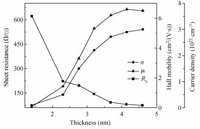
Fig. 1.
Electrical properties of the Cu films deposited on PET substrates with a 20 nm Ga$_{2}$ O$_{3}$ layer.
SEMICONDUCTOR MATERIALS
Huihui Zhuang, Jinliang Yan, Chengyang Xu and Delan Meng
Corresponding author: Yan Jinliang,Email:yanjinliang@yahoo.cn
Abstract: Cu and Cu/ITO films were prepared on polyethylene terephthalate (PET) substrates with a Ga2O3 buffer layer using radio frequency (RF) and direct current (DC) magnetron sputtering. The effect of Cu layer thickness on the optical and electrical properties of the Cu film deposited on a PET substrate with a Ga2O3 buffer layer was studied, and an appropriate Cu layer thickness of 4.2 nm was obtained. Changes in the optoelectrical properties of Cu(4.2 nm)/ITO(30 nm) films were investigated with respect to the Ga2O3 buffer layer thickness. The optical and electrical properties of the Cu/ITO films were significantly influenced by the thickness of the Ga2O3 buffer layer. A maximum transmission of 86%, sheet resistance of 45 Ω/□ and figure of merit of 3.96×10⁻³ Ω -1 were achieved for Cu(4.2 nm)/ITO(30 nm) films with a Ga2O3 layer thickness of 15 nm.
Keywords: transparent conductive films, Ga2O3 buffer layer, Cu/ITO films, optical property, electrical property
| [1] |
Kwon S H, Kang Y M, Cho Y R, et al. Effect of TiO2 buffer layer thickness on properties of ITZO films deposited on flexible substrate. Surface & Coatings Technology, 2010, 205(1):312
|
| [2] |
Chen Yongsheng, Wang Jianhua, Lu Jingxiao, et al. Influence of atomic hydrogen on transparent conducting oxide during hydrogenated microcrystalline Si preparation by PECVD. Chinese Journal of Semiconductors, 2007, 28(7):1005 http://industry.wanfangdata.com.cn/yj/Detail/Periodical?id=Periodical_bdtxb200707001
|
| [3] |
Chen Meng, Bai Xuedong, Huang Rongfang, et al. Structure and conductive mechanism of ITO and AZO films. Chinese Journal of Semiconductors, 2000, 21(4):394
|
| [4] |
Yang Tianlin, Zhang Zhisheng, Song Shumei, et al. Structural, optical and electrical properties of AZO/Cu/AZO tri-layer films prepared by radio frequency magnetron sputtering and ion-beam sputtering. Vacuum, 2009, 83(2):257 http://www.docin.com/p-21757357.html
|
| [5] |
Kim D. Low temperature deposition of transparent conducting ITO/Au/ITO films by reactive magnetron sputtering. Appl Surf Sci, 2010, 256(6):1774 doi: 10.1016/j.apsusc.2009.10.002
|
| [6] |
Szczyrbowski J, Dietrich A, Hartig K. Bendable silver-based low emissivity coating on glass. Solar Energy Mater, 1989, 19(1/2):43
|
| [7] |
Choi K, Kim J, Lee Y, et al. ITO/Ag/ITO multilayer films for the application of a very low resistance transparent electrode. Thin Solid Films, 1999, 341(1/2):152
|
| [8] |
Zhang Huafu, Lei Chengxin, Liu Hanfa, et al. Thickness dependence of the properties of transparent conducting ZnO:Zr films deposited on flexible substrates by RF magnetron sputtering. Journal of Semiconductors, 2009, 30(4):043004 doi: 10.1088/1674-4926/30/4/043004
|
| [9] |
Yu Zhinong, Zhao Jianjian, Xia Fan, et al. Enhanced electrical stability of flexible indium tin oxide films prepared on stripe SiO2 buffer layer coated polymer substrates by magnetron sputtering. Appl Surf Sci, 2011, 257(11):4807 doi: 10.1016/j.apsusc.2010.12.064
|
| [10] |
Xu Linhua, Li Xiangyin, Shi Linxing, et al. Effect of annealing temperature on ZnO thin film grown on a TiO2 buffer Layer. Journal of Semiconductors, 2008, 29(10):1992 http://www.jos.ac.cn/bdtxbcn/ch/reader/view_abstract.aspx?flag=1&file_no=08032502&journal_id=bdtxbcn
|
| [11] |
Li Ting, Yan Jinliang, Ding Xingwei, et al. Effect of substrate temperature on the properties of deep ultraviolet transparent conductive ITO/Ga2O3 films. Journal of Semiconductors, 2012, 33(1):013002 doi: 10.1088/1674-4926/33/1/013002
|
| [12] |
Ueda N, Hosono H, Waseda R, et al. Synthesis and control of conductivity of ultraviolet transmitting β -Ga2O3 single crystals. Appl Phys Lett, 1997, 70(26):3561 doi: 10.1063/1.119233
|
| [13] |
Xiao Ronghui, Zheng Weifeng, Zheng Mingzhi, et al. Influence of thickness on the structural, optical and electrical of Cu films. Journal of Fujian Normal University, 2010, 26(6):49
|
| [14] |
Sahu D R, Huang J L. Characteristics of ZnO-Cu-ZnO multilayer films on copper layer properties. Appl Surf Sci, 2006, 253(2):827 doi: 10.1016/j.apsusc.2006.01.023
|
| [15] |
Natsuhara H, Matsumoto K, Yoshida N, et al. TiO2 thin films as protective material for transparent-conducting oxides used in Si thin film solar cells. Solar Energy Materials & Solar Cells, 2006, 90(17):2867
|
| [16] |
Li Gong, Lu Jianguo, Ye Zhizhen. Transparent conductive Ga-doped ZnO/Cu multilayers prepared on polymer substrates at room temperature. Solar Energy Materials & Solar Cells, 2011, 95(7):1826
|
| [17] |
Ding Xingwei, Yan Jinliang, Li Ting, et al. Effect of SiO2 buffer layer thickness on the properties of ITO/Cu/ITO multilayer films deposited on polyethylene terephthalate substrates. Vacuum, 2011, 86(4):443 doi: 10.1016/j.vacuum.2011.09.005
|
| [18] |
Tsai R Y, Ho F C, Hua M Y. Annealing effects on the properties of indium tin oxide films coated on soda lime glasses with a barrier layer of TiO2-SiO2 composite films. Opt Eng, 1997, 36(8):2335 doi: 10.1117/1.601461
|
| [19] |
Lee J H, Jung H K, Lee J G, et al. Growth and characterization of indium tin oxide thin films deposited on PET substrates. Thin Solid Films, 2008, 516(7):1634 doi: 10.1016/j.tsf.2007.05.028
|
| [20] |
Yu Zhinong, Li Yuqiong, Xia Fan, et al. Properties of indium tin oxide films deposited on unheated polymer substrates by ion beam assisted deposition. Thin Solid Films, 2009, 517(18):5395 doi: 10.1016/j.tsf.2008.12.057
|
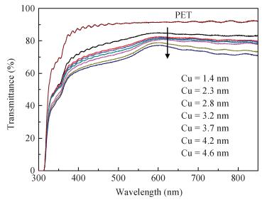
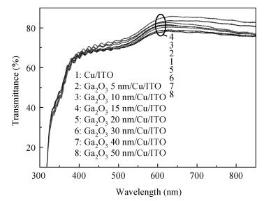
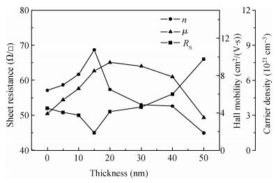
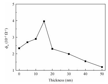
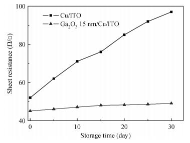
Table 1.
Deposition conditions of ITO, Ga

|
| [1] |
Kwon S H, Kang Y M, Cho Y R, et al. Effect of TiO2 buffer layer thickness on properties of ITZO films deposited on flexible substrate. Surface & Coatings Technology, 2010, 205(1):312
|
| [2] |
Chen Yongsheng, Wang Jianhua, Lu Jingxiao, et al. Influence of atomic hydrogen on transparent conducting oxide during hydrogenated microcrystalline Si preparation by PECVD. Chinese Journal of Semiconductors, 2007, 28(7):1005 http://industry.wanfangdata.com.cn/yj/Detail/Periodical?id=Periodical_bdtxb200707001
|
| [3] |
Chen Meng, Bai Xuedong, Huang Rongfang, et al. Structure and conductive mechanism of ITO and AZO films. Chinese Journal of Semiconductors, 2000, 21(4):394
|
| [4] |
Yang Tianlin, Zhang Zhisheng, Song Shumei, et al. Structural, optical and electrical properties of AZO/Cu/AZO tri-layer films prepared by radio frequency magnetron sputtering and ion-beam sputtering. Vacuum, 2009, 83(2):257 http://www.docin.com/p-21757357.html
|
| [5] |
Kim D. Low temperature deposition of transparent conducting ITO/Au/ITO films by reactive magnetron sputtering. Appl Surf Sci, 2010, 256(6):1774 doi: 10.1016/j.apsusc.2009.10.002
|
| [6] |
Szczyrbowski J, Dietrich A, Hartig K. Bendable silver-based low emissivity coating on glass. Solar Energy Mater, 1989, 19(1/2):43
|
| [7] |
Choi K, Kim J, Lee Y, et al. ITO/Ag/ITO multilayer films for the application of a very low resistance transparent electrode. Thin Solid Films, 1999, 341(1/2):152
|
| [8] |
Zhang Huafu, Lei Chengxin, Liu Hanfa, et al. Thickness dependence of the properties of transparent conducting ZnO:Zr films deposited on flexible substrates by RF magnetron sputtering. Journal of Semiconductors, 2009, 30(4):043004 doi: 10.1088/1674-4926/30/4/043004
|
| [9] |
Yu Zhinong, Zhao Jianjian, Xia Fan, et al. Enhanced electrical stability of flexible indium tin oxide films prepared on stripe SiO2 buffer layer coated polymer substrates by magnetron sputtering. Appl Surf Sci, 2011, 257(11):4807 doi: 10.1016/j.apsusc.2010.12.064
|
| [10] |
Xu Linhua, Li Xiangyin, Shi Linxing, et al. Effect of annealing temperature on ZnO thin film grown on a TiO2 buffer Layer. Journal of Semiconductors, 2008, 29(10):1992 http://www.jos.ac.cn/bdtxbcn/ch/reader/view_abstract.aspx?flag=1&file_no=08032502&journal_id=bdtxbcn
|
| [11] |
Li Ting, Yan Jinliang, Ding Xingwei, et al. Effect of substrate temperature on the properties of deep ultraviolet transparent conductive ITO/Ga2O3 films. Journal of Semiconductors, 2012, 33(1):013002 doi: 10.1088/1674-4926/33/1/013002
|
| [12] |
Ueda N, Hosono H, Waseda R, et al. Synthesis and control of conductivity of ultraviolet transmitting β -Ga2O3 single crystals. Appl Phys Lett, 1997, 70(26):3561 doi: 10.1063/1.119233
|
| [13] |
Xiao Ronghui, Zheng Weifeng, Zheng Mingzhi, et al. Influence of thickness on the structural, optical and electrical of Cu films. Journal of Fujian Normal University, 2010, 26(6):49
|
| [14] |
Sahu D R, Huang J L. Characteristics of ZnO-Cu-ZnO multilayer films on copper layer properties. Appl Surf Sci, 2006, 253(2):827 doi: 10.1016/j.apsusc.2006.01.023
|
| [15] |
Natsuhara H, Matsumoto K, Yoshida N, et al. TiO2 thin films as protective material for transparent-conducting oxides used in Si thin film solar cells. Solar Energy Materials & Solar Cells, 2006, 90(17):2867
|
| [16] |
Li Gong, Lu Jianguo, Ye Zhizhen. Transparent conductive Ga-doped ZnO/Cu multilayers prepared on polymer substrates at room temperature. Solar Energy Materials & Solar Cells, 2011, 95(7):1826
|
| [17] |
Ding Xingwei, Yan Jinliang, Li Ting, et al. Effect of SiO2 buffer layer thickness on the properties of ITO/Cu/ITO multilayer films deposited on polyethylene terephthalate substrates. Vacuum, 2011, 86(4):443 doi: 10.1016/j.vacuum.2011.09.005
|
| [18] |
Tsai R Y, Ho F C, Hua M Y. Annealing effects on the properties of indium tin oxide films coated on soda lime glasses with a barrier layer of TiO2-SiO2 composite films. Opt Eng, 1997, 36(8):2335 doi: 10.1117/1.601461
|
| [19] |
Lee J H, Jung H K, Lee J G, et al. Growth and characterization of indium tin oxide thin films deposited on PET substrates. Thin Solid Films, 2008, 516(7):1634 doi: 10.1016/j.tsf.2007.05.028
|
| [20] |
Yu Zhinong, Li Yuqiong, Xia Fan, et al. Properties of indium tin oxide films deposited on unheated polymer substrates by ion beam assisted deposition. Thin Solid Films, 2009, 517(18):5395 doi: 10.1016/j.tsf.2008.12.057
|


Article views: 2975 Times PDF downloads: 13 Times Cited by: 0 Times
Received: 13 October 2013 Revised: 29 November 2013 Online: Published: 01 May 2014
| Citation: |
Huihui Zhuang, Jinliang Yan, Chengyang Xu, Delan Meng. Effect of Ga2O3 buffer layer thickness on the properties of Cu/ITO thin films deposited on flexible substrates[J]. Journal of Semiconductors, 2014, 35(5): 053001. doi: 10.1088/1674-4926/35/5/053001
****
H H Zhuang, J L Yan, C Y Xu, D L Meng. Effect of Ga2O3 buffer layer thickness on the properties of Cu/ITO thin films deposited on flexible substrates[J]. J. Semicond., 2014, 35(5): 053001. doi: 10.1088/1674-4926/35/5/053001.

|
| [1] |
Kwon S H, Kang Y M, Cho Y R, et al. Effect of TiO2 buffer layer thickness on properties of ITZO films deposited on flexible substrate. Surface & Coatings Technology, 2010, 205(1):312
|
| [2] |
Chen Yongsheng, Wang Jianhua, Lu Jingxiao, et al. Influence of atomic hydrogen on transparent conducting oxide during hydrogenated microcrystalline Si preparation by PECVD. Chinese Journal of Semiconductors, 2007, 28(7):1005 http://industry.wanfangdata.com.cn/yj/Detail/Periodical?id=Periodical_bdtxb200707001
|
| [3] |
Chen Meng, Bai Xuedong, Huang Rongfang, et al. Structure and conductive mechanism of ITO and AZO films. Chinese Journal of Semiconductors, 2000, 21(4):394
|
| [4] |
Yang Tianlin, Zhang Zhisheng, Song Shumei, et al. Structural, optical and electrical properties of AZO/Cu/AZO tri-layer films prepared by radio frequency magnetron sputtering and ion-beam sputtering. Vacuum, 2009, 83(2):257 http://www.docin.com/p-21757357.html
|
| [5] |
Kim D. Low temperature deposition of transparent conducting ITO/Au/ITO films by reactive magnetron sputtering. Appl Surf Sci, 2010, 256(6):1774 doi: 10.1016/j.apsusc.2009.10.002
|
| [6] |
Szczyrbowski J, Dietrich A, Hartig K. Bendable silver-based low emissivity coating on glass. Solar Energy Mater, 1989, 19(1/2):43
|
| [7] |
Choi K, Kim J, Lee Y, et al. ITO/Ag/ITO multilayer films for the application of a very low resistance transparent electrode. Thin Solid Films, 1999, 341(1/2):152
|
| [8] |
Zhang Huafu, Lei Chengxin, Liu Hanfa, et al. Thickness dependence of the properties of transparent conducting ZnO:Zr films deposited on flexible substrates by RF magnetron sputtering. Journal of Semiconductors, 2009, 30(4):043004 doi: 10.1088/1674-4926/30/4/043004
|
| [9] |
Yu Zhinong, Zhao Jianjian, Xia Fan, et al. Enhanced electrical stability of flexible indium tin oxide films prepared on stripe SiO2 buffer layer coated polymer substrates by magnetron sputtering. Appl Surf Sci, 2011, 257(11):4807 doi: 10.1016/j.apsusc.2010.12.064
|
| [10] |
Xu Linhua, Li Xiangyin, Shi Linxing, et al. Effect of annealing temperature on ZnO thin film grown on a TiO2 buffer Layer. Journal of Semiconductors, 2008, 29(10):1992 http://www.jos.ac.cn/bdtxbcn/ch/reader/view_abstract.aspx?flag=1&file_no=08032502&journal_id=bdtxbcn
|
| [11] |
Li Ting, Yan Jinliang, Ding Xingwei, et al. Effect of substrate temperature on the properties of deep ultraviolet transparent conductive ITO/Ga2O3 films. Journal of Semiconductors, 2012, 33(1):013002 doi: 10.1088/1674-4926/33/1/013002
|
| [12] |
Ueda N, Hosono H, Waseda R, et al. Synthesis and control of conductivity of ultraviolet transmitting β -Ga2O3 single crystals. Appl Phys Lett, 1997, 70(26):3561 doi: 10.1063/1.119233
|
| [13] |
Xiao Ronghui, Zheng Weifeng, Zheng Mingzhi, et al. Influence of thickness on the structural, optical and electrical of Cu films. Journal of Fujian Normal University, 2010, 26(6):49
|
| [14] |
Sahu D R, Huang J L. Characteristics of ZnO-Cu-ZnO multilayer films on copper layer properties. Appl Surf Sci, 2006, 253(2):827 doi: 10.1016/j.apsusc.2006.01.023
|
| [15] |
Natsuhara H, Matsumoto K, Yoshida N, et al. TiO2 thin films as protective material for transparent-conducting oxides used in Si thin film solar cells. Solar Energy Materials & Solar Cells, 2006, 90(17):2867
|
| [16] |
Li Gong, Lu Jianguo, Ye Zhizhen. Transparent conductive Ga-doped ZnO/Cu multilayers prepared on polymer substrates at room temperature. Solar Energy Materials & Solar Cells, 2011, 95(7):1826
|
| [17] |
Ding Xingwei, Yan Jinliang, Li Ting, et al. Effect of SiO2 buffer layer thickness on the properties of ITO/Cu/ITO multilayer films deposited on polyethylene terephthalate substrates. Vacuum, 2011, 86(4):443 doi: 10.1016/j.vacuum.2011.09.005
|
| [18] |
Tsai R Y, Ho F C, Hua M Y. Annealing effects on the properties of indium tin oxide films coated on soda lime glasses with a barrier layer of TiO2-SiO2 composite films. Opt Eng, 1997, 36(8):2335 doi: 10.1117/1.601461
|
| [19] |
Lee J H, Jung H K, Lee J G, et al. Growth and characterization of indium tin oxide thin films deposited on PET substrates. Thin Solid Films, 2008, 516(7):1634 doi: 10.1016/j.tsf.2007.05.028
|
| [20] |
Yu Zhinong, Li Yuqiong, Xia Fan, et al. Properties of indium tin oxide films deposited on unheated polymer substrates by ion beam assisted deposition. Thin Solid Films, 2009, 517(18):5395 doi: 10.1016/j.tsf.2008.12.057
|

 WeChat ID
Journal of Semiconductors © 2017 All Rights Reserved 京ICP备05085259号-2

 DownLoad:

